EP1041533A1 - Semiconductor device including a power supply, and liquid crystal device and electronic equipment using the same - Google Patents

Semiconductor device including a power supply, and liquid crystal device and electronic equipment using the same Download PDF

Info

Publication number
EP1041533A1
EP1041533A1 EP00106090A EP00106090A EP1041533A1 EP 1041533 A1 EP1041533 A1 EP 1041533A1 EP 00106090 A EP00106090 A EP 00106090A EP 00106090 A EP00106090 A EP 00106090A EP 1041533 A1 EP1041533 A1 EP 1041533A1
Authority
EP
European Patent Office
Prior art keywords
potential
power supply
circuit
mos transistor
type
Prior art date
Legal status (The legal status is an assumption and is not a legal conclusion. Google has not performed a legal analysis and makes no representation as to the accuracy of the status listed.)
Withdrawn
Application number
EP00106090A
Other languages
German (de)
French (fr)
Inventor
Norio Koizumi
Current Assignee (The listed assignees may be inaccurate. Google has not performed a legal analysis and makes no representation or warranty as to the accuracy of the list.)
Seiko Epson Corp
Original Assignee
Seiko Epson Corp
Priority date (The priority date is an assumption and is not a legal conclusion. Google has not performed a legal analysis and makes no representation as to the accuracy of the date listed.)
Filing date
Publication date
Application filed by Seiko Epson Corp filed Critical Seiko Epson Corp
Publication of EP1041533A1 publication Critical patent/EP1041533A1/en
Withdrawn legal-status Critical Current

Links

Images

Classifications

    • GPHYSICS
    • G09EDUCATION; CRYPTOGRAPHY; DISPLAY; ADVERTISING; SEALS
    • G09GARRANGEMENTS OR CIRCUITS FOR CONTROL OF INDICATING DEVICES USING STATIC MEANS TO PRESENT VARIABLE INFORMATION
    • G09G3/00Control arrangements or circuits, of interest only in connection with visual indicators other than cathode-ray tubes
    • G09G3/20Control arrangements or circuits, of interest only in connection with visual indicators other than cathode-ray tubes for presentation of an assembly of a number of characters, e.g. a page, by composing the assembly by combination of individual elements arranged in a matrix no fixed position being assigned to or needed to be assigned to the individual characters or partial characters
    • G09G3/34Control arrangements or circuits, of interest only in connection with visual indicators other than cathode-ray tubes for presentation of an assembly of a number of characters, e.g. a page, by composing the assembly by combination of individual elements arranged in a matrix no fixed position being assigned to or needed to be assigned to the individual characters or partial characters by control of light from an independent source
    • G09G3/36Control arrangements or circuits, of interest only in connection with visual indicators other than cathode-ray tubes for presentation of an assembly of a number of characters, e.g. a page, by composing the assembly by combination of individual elements arranged in a matrix no fixed position being assigned to or needed to be assigned to the individual characters or partial characters by control of light from an independent source using liquid crystals
    • G09G3/3611Control of matrices with row and column drivers
    • G09G3/3674Details of drivers for scan electrodes
    • GPHYSICS
    • G09EDUCATION; CRYPTOGRAPHY; DISPLAY; ADVERTISING; SEALS
    • G09GARRANGEMENTS OR CIRCUITS FOR CONTROL OF INDICATING DEVICES USING STATIC MEANS TO PRESENT VARIABLE INFORMATION
    • G09G3/00Control arrangements or circuits, of interest only in connection with visual indicators other than cathode-ray tubes
    • G09G3/20Control arrangements or circuits, of interest only in connection with visual indicators other than cathode-ray tubes for presentation of an assembly of a number of characters, e.g. a page, by composing the assembly by combination of individual elements arranged in a matrix no fixed position being assigned to or needed to be assigned to the individual characters or partial characters
    • G09G3/34Control arrangements or circuits, of interest only in connection with visual indicators other than cathode-ray tubes for presentation of an assembly of a number of characters, e.g. a page, by composing the assembly by combination of individual elements arranged in a matrix no fixed position being assigned to or needed to be assigned to the individual characters or partial characters by control of light from an independent source
    • G09G3/36Control arrangements or circuits, of interest only in connection with visual indicators other than cathode-ray tubes for presentation of an assembly of a number of characters, e.g. a page, by composing the assembly by combination of individual elements arranged in a matrix no fixed position being assigned to or needed to be assigned to the individual characters or partial characters by control of light from an independent source using liquid crystals
    • G09G3/3611Control of matrices with row and column drivers
    • G09G3/3685Details of drivers for data electrodes
    • GPHYSICS
    • G09EDUCATION; CRYPTOGRAPHY; DISPLAY; ADVERTISING; SEALS
    • G09GARRANGEMENTS OR CIRCUITS FOR CONTROL OF INDICATING DEVICES USING STATIC MEANS TO PRESENT VARIABLE INFORMATION
    • G09G3/00Control arrangements or circuits, of interest only in connection with visual indicators other than cathode-ray tubes
    • G09G3/20Control arrangements or circuits, of interest only in connection with visual indicators other than cathode-ray tubes for presentation of an assembly of a number of characters, e.g. a page, by composing the assembly by combination of individual elements arranged in a matrix no fixed position being assigned to or needed to be assigned to the individual characters or partial characters
    • G09G3/34Control arrangements or circuits, of interest only in connection with visual indicators other than cathode-ray tubes for presentation of an assembly of a number of characters, e.g. a page, by composing the assembly by combination of individual elements arranged in a matrix no fixed position being assigned to or needed to be assigned to the individual characters or partial characters by control of light from an independent source
    • G09G3/36Control arrangements or circuits, of interest only in connection with visual indicators other than cathode-ray tubes for presentation of an assembly of a number of characters, e.g. a page, by composing the assembly by combination of individual elements arranged in a matrix no fixed position being assigned to or needed to be assigned to the individual characters or partial characters by control of light from an independent source using liquid crystals
    • G09G3/3611Control of matrices with row and column drivers
    • G09G3/3696Generation of voltages supplied to electrode drivers
    • GPHYSICS
    • G09EDUCATION; CRYPTOGRAPHY; DISPLAY; ADVERTISING; SEALS
    • G09GARRANGEMENTS OR CIRCUITS FOR CONTROL OF INDICATING DEVICES USING STATIC MEANS TO PRESENT VARIABLE INFORMATION
    • G09G2300/00Aspects of the constitution of display devices
    • G09G2300/04Structural and physical details of display devices
    • G09G2300/0404Matrix technologies
    • G09G2300/0408Integration of the drivers onto the display substrate
    • GPHYSICS
    • G09EDUCATION; CRYPTOGRAPHY; DISPLAY; ADVERTISING; SEALS
    • G09GARRANGEMENTS OR CIRCUITS FOR CONTROL OF INDICATING DEVICES USING STATIC MEANS TO PRESENT VARIABLE INFORMATION
    • G09G2310/00Command of the display device
    • G09G2310/02Addressing, scanning or driving the display screen or processing steps related thereto
    • G09G2310/0264Details of driving circuits
    • G09G2310/0289Details of voltage level shifters arranged for use in a driving circuit
    • GPHYSICS
    • G09EDUCATION; CRYPTOGRAPHY; DISPLAY; ADVERTISING; SEALS
    • G09GARRANGEMENTS OR CIRCUITS FOR CONTROL OF INDICATING DEVICES USING STATIC MEANS TO PRESENT VARIABLE INFORMATION
    • G09G2330/00Aspects of power supply; Aspects of display protection and defect management
    • G09G2330/02Details of power systems and of start or stop of display operation
    • G09G2330/027Arrangements or methods related to powering off a display

Definitions

  • the present invention relates to a semiconductor device with a power supply circuit mounted thereon, and a liquid crystal device and electronic equipment using the semiconductor device. Particularly, the present invention relates to a technique for the prevention of malfunctions which may occur in the case of power supply emergencies, such as in the case where a battery is taken out.
  • liquid crystal device such as a liquid crystal display
  • a display operation is implemented when a voltage is applied to liquid crystals which are sealed between substrates in which electrodes are formed.
  • This type of liquid crystal display has been widely used in recent years in various electronic equipment such as personal computers, word processors, cellular phones, electronic pocketbooks, and the like.
  • Such electronic equipment using a liquid crystal display is designed so that the screen becomes blank instantaneously when the power source is cut off according to a prescribed sequence.
  • the phenomenon of instantaneous lighting occurs when the display is turned off by a procedure other than the above-described sequence, such as the case in which the battery is abruptly drawn out during the display operation, or the electronic equipment is forcedly terminated. Specifically, in this phenomenon the screen image instantaneously disappears when the battery is drawn out during display, following which lighting images such as horizontal lines appear for a while.
  • the present inventors have conducted extensive studies concerning the instantaneous lighting phenomenon and have achieved the present invention.
  • an objective of the present invention is to provide a semiconductor device with a power supply circuit mounted thereon, which can prevent malfunctions such as instantaneous lighting which occurs at the time of power supply emergencies, and a liquid crystal device and electronic equipment using the semiconductor device.
  • a semiconductor device including a drive circuit, a drive control circuit which controls the drive circuit, and a power supply circuit which supplies a potential to the drive circuit and drive control circuit, wherein the power supply circuit comprises:
  • the first potential and the second potential which are supplied from external power supply sources become equal, e.g. the same potential as the ground potential, after a certain period of time.
  • the drive circuit changes all potentials outputted from the drive circuit to a value equivalent to the first power supply potential (the ground potential) based on the signals which becomes active when a power supply emergency occurs. This causes all devices which are operated by a potential supplied by the semiconductor device to be completely shutoff without malfunction.
  • a semiconductor device including a drive circuit, a drive control circuit which controls the drive circuit, and a power supply circuit which supplies a potential to the drive circuit and drive control circuit, wherein the power supply circuit comprises:
  • the operation of the drive circuit in the first-mentioned aspect in the event of a power supply emergency is performed based on the potential selection signals from the drive control circuit.
  • the drive control circuit preferably comprises:
  • This constitution of the drive control circuit ensures that both the first and the second logic levels from the logic circuit after a battery is drawn out become the same ground potential as each other.
  • the output from the level shifter group may become indefinite, this can be controlled as described above, whereby occurrence of malfunctions can be prevented.
  • the level shifter group has an input level setting circuit for setting the input to the level shifters at a specified value based on the signals which become active in the event of a power supply emergency regardless of the output of the logic circuit.
  • indefinite output of the level shifter group can be prevented by setting the input to the level shifters at a specified value in the event of a power supply emergency. Malfunctions can then be prevented by controlling the device in the manner described above based on the specified value inputted to the level shifter group.
  • the potential selection circuit has an output level setting circuit for setting the output of the potential selection circuit at a specified value based on the signals which become active in the event of a power supply emergency regardless of the output of the level shifter group.
  • indefinite output of the level shifter group can be prevented by setting the output of the level shifters to a specified value in the event of power supply emergencies. Malfunctions can then be prevented by controlling the device in the manner described above based on the specified value outputted from the level shifters.
  • the signals activated in the event of a power supply emergency may be outputs from a comparator provided in the semiconductor device or power-on reset signals supplied from outside the semiconductor device.
  • a semiconductor device including a drive circuit, a drive control circuit which controls the drive circuit, and a power supply circuit which supplies a potential to the drive circuit and drive control circuit, wherein the power supply circuit comprises:
  • Another cause of malfunction such as instantaneous lighting is a situation where the output from level shifters composing the shift level group becomes indefinite according to the input in the event of a power supply emergency.
  • the potential maintaining circuit which is provided in each level shifter maintains the first and the second output potentials of the level shifter which existed prior to the occurrence of a power supply emergency.
  • the output of the level shifter group does not become indefinite at the time of a power supply emergency, whereby malfunctions due to a power supply emergency can be prevented.
  • the potential maintaining circuit provided in each of the level shifters forming the level shifter group may comprise:
  • the second output potential may be supplied to a gate of the third MOS transistor of primary conductive-type, and the first output potential may be supplied to a gate of the fourth MOS transistor of primary conductive-type.
  • both the first and the second logic levels from the logic circuit become the same ground potentials as each other, after a battery is drawn out, for instance.
  • both the first and the second MOS transistors of primary conductive-type of the level shifter are either "on” or "off".
  • the potential maintaining circuit turns either one of the third and fourth MOS transistors of primary conductive-type "on” and the other "off” at the time of a power supply emergency. Specifically, when the state of first MOS transistor of primary conductive-type after a power supply emergency varies from the state before the power supply emergency, the first output potential causes the state of the third MOS transistor of primary conductive-type connected in parallel to be identical to the state of the first MOS transistor of primary conductive-type before the power supply emergency.
  • the second output potential causes the state of the fourth MOS transistor of primary conductive-type connected in parallel to become identical to the state of second MOS transistor of primary conductive-type before the power supply emergency.
  • the first and the second output potentials from the level shifter before and after a power supply emergency can be maintained equivalent by this action.
  • the previous output conditions can thus be maintained even when the first and the second logic levels from the logic circuit take the same logic conditions. Therefore, the first and the second output potentials from the level shifter can be fixed after a cutoff of the power supply.
  • the drive circuit may cause all output potentials to become identical, for example, to the first power supply potential, whereby occurrence of malfunctions can be prevented.
  • the potential maintaining circuit provided in at least one of the level shifters forming the level shifter group includes a third MOS transistor of primary conductive-type connected in parallel to the first MOS transistor of primary conductive-type, and, when an on/off state of the first MOS transistor of primary conductive-type changes before and after the power supply emergency, the on/off state of the third MOS transistor of primary conductive-type is set identical to an on/off state of the first MOS transistor of primary conductive-type which existed before the power supply emergency.
  • the on/off state of the first MOS transistor of primary conductive-type varies before and after the power supply emergency in at least one level shifter.
  • malfunctions can be prevented by setting the state of the third MOS transistor of primary conductive-type connected in parallel to the first MOS transistor of primary conductive-type to a state identical to that of the first MOS transistor of primary conductive-type before the power supply emergency.
  • the potential maintaining circuit provided in at least one of the level shifters forming the level shifter group includes a fourth MOS transistor of primary conductive-type connected in parallel to the second MOS transistor of primary conductive-type, and, when an on/off state of the second MOS transistor of primary conductive-type changes before and after the power supply emergency, the on/off state of the fourth MOS transistor of primary conductive-type after the power supply emergency is set identical to an on/off state of the second MOS transistor of primary conductive-type before the power supply emergency.
  • the on/off state of the second MOS transistor of primary conductive-type varies before the power supply emergency in at least one level shifter.
  • malfunctions can be prevented by setting the state of the third MOS transistor of primary conductive-type connected in parallel to the second MOS transistor of primary conductive-type to a state identical to that of the second MOS transistor of primary conductive-type before the power supply emergency.
  • the present invention can be applied to a liquid crystal device and electronic equipment using the above-described semiconductor device, and can reliably prevent malfunctions which may occur in the case of a power supply emergency, such as the case where a battery is taken out.
  • FIG. 1 shows a constitution of major parts of a liquid crystal device
  • FIG. 2 is an example of a waveform chart showing a drive waveform for driving the liquid crystal panel of FIG. 1.
  • a liquid crystal panel for example, a simple matrix pattern liquid crystal panel 10, is formed by sealing liquid crystals between a first substrate in which common electrodes CO to Cm are formed, and a second substrate in which segment electrodes S0 to Sn are formed.
  • the point at which one common electrode and one segment electrode cross is a display pixel.
  • the liquid crystal panel 10 has (m + 1) x (n + 1) display pixels.
  • liquid crystal panel such as an active matrix pattern liquid crystal display panel can be used instead of the simple matrix pattern liquid crystal panel 10 in this example.
  • a common driver 22 connected with the common electrodes C0 to Cm, and a segment driver 24 connected with the segment electrodes S0 to Sn are provided.
  • the common driver 22 and segment driver 24 are supplied with a prescribed voltage from a power supply circuit 30, and selectively supply this prescribed voltage to the common electrodes C0 to Cm or the segment electrodes S0 to Sn in accordance with signals from the drive control circuit 40.
  • FIG. 2 shows an example of a drive waveform during a frame period in which the common electrode C3 in the liquid crystal panel 10 in FIG. 1 is selected.
  • the thick solid line indicates the drive waveform supplied to each of the common electrodes C0 to Cm from the common driver 22, whereas the thin solid line indicates the drive waveform supplied to each of the segment electrodes S0 to Sn from the segment driver 24.
  • the polarity of the voltage applied to the liquid crystal in FIG. 2 is inverted from positive to negative, or vice versa, according to the polarity conversion signal FR. For this reason, six levels of drive potential V0 to V5 are used.
  • the drive waveform supplied by the common driver 22 varies among the potentials V0, V 1, V4, and V5.
  • the drive waveform supplied by the segment driver 24 varies among the potentials V0, V 2, V3, and V5.
  • FIG. 3 shows details of a single chip semiconductor device comprising a drive circuit 20, a power supply circuit 30, and a drive control circuit 40 of FIG. 1.
  • the present invention can be applied also to a configuration in which the drive circuit 20, power supply circuit 30, and drive control circuit 40 are mounted on a plurality of chips respectively.
  • the power supply circuit 30 produces V1 to V5 based on the first power supply potential VDD and the second power supply potential VSS.
  • the power supply circuit 30 has a first logic circuit 31, first to third level shifters 32 to 34, a boosting circuit 35, a constant current circuit 36, a regulator 37, and a voltage follower circuit 38.
  • the constant current circuit 36, regulator 37, and voltage follower circuit 38 function as a bias generating circuit.
  • the drive control circuit 40 has a second logic circuit 41, a fourth level shifter group 42, and a potential selection circuit 43.
  • the first to third level shifters 32 to 34 shift the levels of the logic output I and the inverted output XI of the first logic circuit 31, and the fourth level shifter group 42 shifts the levels of the logic output I and the inverted output XI of the second logic circuit 41.
  • the potential selection circuit 43 in the drive control circuit 40 sends signals to the drive circuit 20 instructing which of the potentials V0 to V5 should be supplied to the common electrode and the segment electrode according to the outputs from the fourth level shifter group 42.
  • 3V
  • the voltage applied to the liquid crystal differs according to the drive duty. For example, if the duty is 1/32, 5V to 7V is required, and if the duty is 1/64, 8V to 12V is required. In either case, the voltage is insufficient if
  • 3V .
  • a boosting circuit 35 and a constant current circuit 36 are provided in the drive circuit 30, to boost
  • 3V and produce VOUT.
  • VOUT -9V.
  • the regulator 37 produces a stable constant potential V5 based on the VOUT.
  • the voltage follower circuit 38 has a resistance dividing circuit 38A and first to fourth differential amplifiers 38B to 38E as shown in FIG. 5, for example.
  • a capacitor is provided between the supply line for voltage V0 and each of the supply lines for voltages V1 to V5 and Vout.
  • FIG. 7 shows a constitution of a circuit for supplying voltage to the segment electrodes S0 to Sm of the display part 10
  • FIG. 8 shows a constitution of a circuit for supplying voltage to the common electrodes C0 to Cn of the display part 10.
  • a level shifter 42A, a potential selection block 43A, and switches SW1, SW4 to SW6 are provided as a voltage supply system for one segment electrode.
  • a level shifter 42B which is common to the supply system for all segment electrodes is provided in the circuit of FIG. 7.
  • the potential selection block 43A is provided with first to fourth logic gates 44A to 44D which controls turning on and off of the switches SW1 and SW4 to SW6 according to the outputs of the level shifters 42A and 42B.
  • the system supplying voltage to one common electrode shown in FIG. 8 is provided with a level shifter 42C, a potential selection block 43B, and switches SW1 to SW4.
  • a level shifter 42D which is common to the supply system for all common electrodes is also provided in the constitution of FIG. 8.
  • the potential selection block 43B is provided with first to fourth logic gates 45A to 45D which controls turning on and off of the switches SW1 to SW4 according to the outputs of the level shifters 42C and 42D.
  • the level shifters 42A to 42D, etc. which constitutes the fourth level shifter group shown in FIG. 3 will now be described referring FIG. 9.
  • the level shifters constituting the fourth level shifter group has first and second circuits 55 and 65 connected in parallel to each other.
  • An output I from the second logic circuit 41 shown in FIG. 2 is supplied to the gate of the first P-type MOS transistor 50 and the gate of the first N-type MOS transistor 51.
  • a second P-type MOS transistor 60, a third N-type MOS transistor 61, and a fourth N-type MOS transistor 62 are connected in series, whereby a second circuit 65 is formed.
  • An inverted output XI from the second logic circuit 41 shown in FIG. 2 is supplied to the gate of the second P-type MOS transistor 60 and the gate of the third N-type MOS transistor 61.
  • the potential between the first P-type MOS transistor 50 and the first N-type MOS transistor 51 is the inverted output XO of the level shifter 42
  • the potential between the second P-type MOS transistor 60 and the third N-type MOS transistor 61 is the output O of the level shifter 42.
  • the inverted output XO is supplied to the gate of the fourth N-type MOS transistor 62
  • the output O is supplied to the gate of the second N-type MOS transistor 52.
  • Input-output characteristics of the level shifter shown in FIG. 9 are shown in the following Table 3.
  • V5 generated from VOUT shown in FIG. 2 also changes to VDD, this change from V5 to VDD (V5 ⁇ VDD) is slower than the change from VSS to VDD (VSS ⁇ VDD).
  • FIG. 10 shows details of a conventional triple boosting circuit 35.
  • an output O of the third level shifter 34 is supplied to the gates of the first and third N-type MOS transistors 81 and 83, and an output XO of the third level shifter 34 is supplied to the gate of the second N-type MOS transistor 82.
  • This boosting circuit 35 has capacitors C1 to C3 which are charged by N to type MOS transistors 81 to 83, of which on/off operation is controlled by the output O and output XO of the third level shifter 34.
  • the output potential VOUT is determined by the amount of the charge provided to the capacitor C3.
  • the potential of the output O is decreased to an intermediate level by the on/off operations of the second P-type MOS transistor 60 and the third N-type MOS transistor 61 which are shown in FIG. 9. Finally, the second N-type MOS transistor 52 is turned “off” from “on”. The potential of the output XO thus increases.
  • FIGS. 11 and 12 show segment and common electrode systems in the embodiment of the present invention, in which improved level shifters are used rather than the conventional level shifters shown in FIGS. 7 and 8.
  • the segment electrode drive system and common electrode drive system are provided with a comparator 100, a reference potential generating circuit 101, and a buffer 102A, all used in common with these drives.
  • a P-type MOS transistor 103 is provided between an input line connected to the input terminal I of the level shifter 42A and a supply line for the first power supply potential VDD, as shown in FIG. 11.
  • a P-type MOS transistor 104 is provided between an input line connected to the input terminal I of the level shifter 42B and a supply line for the first power supply potential VDD, as shown also in FIG. 11.
  • a P-type MOS transistor 105 is provided between an input line connected to the input terminal I of the level shifter 42C and a supply line for the first power supply potential VDD, as shown in FIG. 12.
  • a P-type MOS transistor 106 is provided between an input line connected to the input terminal I of the level shifter 42D and a supply line for the first power supply potential VDD, as shown also in FIG. 12.
  • a reference potential VREG is input to the input terminal of the comparator 100, whereas a second power supply potential VSS is input to the inverted input terminal.
  • VREG is -1.8V, for example.
  • the reference potential generating circuit 101 is made up of one or more N-type MOS transistors which are connected in series and can produce the reference potential VREG by causing the voltage of the first power supply potential VDD to be reduced by the threshold voltage Vth of each transistor.
  • HIGH is outputted under normal conditions in which the second power supply potential VSS is lower than the reference potential VREG
  • LOW is outputted in the case such as when the power supply is forcibly cut off, in which case the second power supply potential VSS is higher than the reference potential VREG.
  • the output of the buffer 102A is also HIGH (VDD) when the power supply potential is normal, and is LOW (V5) when the power supply potential is abnormal.
  • the comparator 100, reference potential generating circuit 101, and buffer 102A do not necessarily have to be provided in the semiconductor device with the power supply circuit 30 and the like mounted thereon. Instead of using the output from the buffer 102A, it is possible to supply pour-on-reset signals from outside the semiconductor device to the gate of the fourth P-type MOS transistor 63.
  • the power-on-reset signals are detector outputs which always detect potentials of external power supplies and become active when the power supply potential falls below a prescribed value. Therefore, if the power-on-reset signal is LOW active, this is equivalent to the output of the buffer 102A.
  • the output of the buffer 102A becomes LOW (V5) and all four P-type MOS transistors 103 to 106 are turned on, as mentioned above. Therefore, regardless of the logic of signals IA to ID, HIGH (VDD) is inputted in the input terminal I of the level shifters 42A to 42C and LOW (V5) is inputted to the input terminal XI. In addition, LOW (V5) is inputted in the input terminal I of the level shifter 42D and HIGH (VDD) is input to the input terminal XI.
  • P-type MOS transistors 103 to 106 have a low "ON" resistance (a high capacity).
  • FIGS. 14 and 15 respectively show a segment electrode drive system and common electrode drive system for a potential selection circuit 43 with which countermeasures against instantaneous lighting is provided.
  • the segment electrode drive system shown in FIG. 14 is provided with first to fifth logic gates 46A to 46E which control switches SW1 and SW4 to SW6 on-and-off according to the outputs from the level shifter 42A, 42B, comparator 100, and inversion element 102B.
  • the common electrode drive system shown in FIG. 15 is provided with first to fifth logic gates 47A to 47E which control switches SW1 to SW4 on-and-off according to the outputs from the level shifter 42A, 42B, comparator 100, and inversion element 102B.
  • FIG. 16 and FIG. 17 An unproved structured of a final output stage of the drive circuit 20 of FIG. 3 is shown in FIG. 16 and FIG. 17. As shown in FIG. 16 and FIG. 17, all common electrodes C0 to Cn and all segment electrodes S0 to Sm are respectively connected to a P-type MOS transistor 300. In addition, the segment electrode drive system and common electrode drive system shown in FIG. 16 and FIG. 17 are provided with a comparator 100, a reference potential generating circuit 101, and a buffer 102A, all used in common with these drives systems.
  • each P-type MOS transistor 300 must have a lower “on"-resistance (higher capacity) than the MOS transistors constituting switches SW1 to SW6.
  • "on"-resistance of switches SW1 to SW6 is 1 to 2 K ⁇
  • "on"-resistance of the P-type MOS transistors 103 to 106 should be several tens of ⁇ .
  • each of the level shifters constituting the fourth level shifter group 42 has the first and the second circuits 55 and 65 which are connected in parallel to each other.
  • An output I from the second logic circuit 41 shown in FIG. 2 is supplied to the gate of the first P-type MOS transistor 50 and the gate of the first N-type MOS transistor 51.
  • a second P-type MOS transistor 60, a third N-type MOS transistor 61, and a fourth N-type MOS transistor 62 are connected in series, whereby a second circuit 65 is formed.
  • An inverted output XI from the second logic circuit 41 shown in FIG. 2 is supplied to the gate of the second P-type MOS transistor 60 and the gate of the third N-type MOS transistor 61.
  • the potential between the first P-type MOS transistor 50 and the first N-type MOS transistor 51 is the inverted output XO of the level shifter 42
  • the potential between the second P-type MOS transistor 60 and the third N-type MOS transistor 61 is the output O of the level shifter 42.
  • the inverted output XO is supplied to the gate of the fourth N-type MOS transistor 62
  • the output O is supplied to the gate of the second N-type MOS transistor 52.
  • a third P-type MOS transistor 53 is provided parallel to the first P-type MOS transistor 50, and a fourth P-type MOS transistor 63 is provided parallel to the second P-type MOS transistor 60.
  • the inverted output XO is supplied to the gate of the fourth P-type MOS transistor 63, and the output O is supplied to the gate of the third P-type MOS transistor 53.
  • the outputs (O, XO) of the level shifters 42A to 42C in the fourth level shifter group 42 in the embodiment shown in FIG. 19 can be set to the output conditions (VDD, V5) which were effective before the power supply shut-off.
  • the output will not become indefinite as in the case of the conventional level shifters shown in FIG. 9.
  • each level shifter 42A to 42D in FIG. 7 and FIG. 8 can be operated in a normal manner to continue supply of potential V0 to all common and segment electrodes as shown in FIG. 20. Instantaneous lighting can thus be prevented.
  • FIG. 21 and FIG. 22 are modified examples of the level shifter provided with measures for preventing malfunctions due to instantaneous lighting.
  • a fourth P-type MOS transistor 63 is provided being connected parallel with the second P-type MOS transistor 60, but the third P-type MOS transistor 53 is not provided.
  • a third P-type MOS transistor 53 is provided being connected parallel with the first P-type MOS transistor 50, but the fourth P-type MOS transistor 63 is not provided.
  • the gate of the fourth P-type MOS transistor 63 in FIG. 21 and the gate of the third P-type MOS transistor 53 in FIG. 22 are supplied with the output of the comparator 100 which was described in the above described embodiment. Because the output of the comparator 100 is the same as that shown in FIG. 13, the fourth P-type MOS transistor 63 in FIG. 21 and the third P-type MOS transistor 53 in FIG. 22 are turned “ on" at the time of a power supply emergency.
  • the second power supply potential which was a negative potential in the embodiments described above may be a positive potential.
  • the present invention can be applied to various types of electronic equipment such as cellular phones, game machines, electronic pocketbooks, personal computers, word processor equipment, navigation devices, and the like on which the liquid crystal panel 10 shown in FIG. 1 is mounted.
  • electronic equipment such as cellular phones, game machines, electronic pocketbooks, personal computers, word processor equipment, navigation devices, and the like on which the liquid crystal panel 10 shown in FIG. 1 is mounted.

Abstract

A semiconductor device capable of preventing malfunctions of instantaneous lighting, and comprises a drive circuit, a drive control circuit, and a power supply circuit. The power supply circuit has a boosting circuit which is provided with a first power supply potential VDD being a ground potential from an external power supply and a second power supply potential VSS, being a potential other than the ground potential, and raises the absolute value of the second power supply potential VSS and charges to the capacitor; and a bias generating circuit generating a potential to be supplied to the drive circuit and drive control circuit based on the output potential of the boosting circuit. A first power supply potential VDD and the potential of the bias generating circuits are supplied to the drive circuit which outputs a potential selected from the potentials V0 to V5 supplied in accordance with the control of the drive control circuit during a normal power supply period, and, during a power supply emergency, in which the absolute value between the first and the second potentials VDD and VSS becomes lower than a prescribed vale, tuns on a P-type MOS transistor based on a LOW active signal from a buffer, whereby all potentials output from the drive circuit are forcibly set to the first power supply potential VDD.

Description

    BACKGROUND OF THE INVENTION Field of the Invention
  • The present invention relates to a semiconductor device with a power supply circuit mounted thereon, and a liquid crystal device and electronic equipment using the semiconductor device. Particularly, the present invention relates to a technique for the prevention of malfunctions which may occur in the case of power supply emergencies, such as in the case where a battery is taken out.
  • Description of the Related Art
  • In a liquid crystal device such as a liquid crystal display, a display operation is implemented when a voltage is applied to liquid crystals which are sealed between substrates in which electrodes are formed. This type of liquid crystal display has been widely used in recent years in various electronic equipment such as personal computers, word processors, cellular phones, electronic pocketbooks, and the like.
  • Such electronic equipment using a liquid crystal display is designed so that the screen becomes blank instantaneously when the power source is cut off according to a prescribed sequence. The phenomenon of instantaneous lighting occurs when the display is turned off by a procedure other than the above-described sequence, such as the case in which the battery is abruptly drawn out during the display operation, or the electronic equipment is forcedly terminated. Specifically, in this phenomenon the screen image instantaneously disappears when the battery is drawn out during display, following which lighting images such as horizontal lines appear for a while.
  • The present inventors have conducted extensive studies concerning the instantaneous lighting phenomenon and have achieved the present invention.
  • SUMMARY OF THE INVENTION
  • Accordingly, an objective of the present invention is to provide a semiconductor device with a power supply circuit mounted thereon, which can prevent malfunctions such as instantaneous lighting which occurs at the time of power supply emergencies, and a liquid crystal device and electronic equipment using the semiconductor device.
  • In one aspect of the present invention, a semiconductor device including a drive circuit, a drive control circuit which controls the drive circuit, and a power supply circuit which supplies a potential to the drive circuit and drive control circuit,
       wherein the power supply circuit comprises:
  • a boosting circuit, to which a first power supply potential which is a ground potential from an external power supply and a second power supply potential which is a potential other than the ground potential are supplied, and raising the absolute value of the second power supply potential and charging the boosted potential to the capacitor; and
  • a bias generating circuit generating a potential supplied to the drive circuit and the drive control circuit based on the output potential of the boosting circuit, and
    wherein the first power supply potential and a potential from the bias generating circuit are supplied to the drive circuit that outputs a potential selected from potentials supplied in accordance with a control of the drive control circuit during a normal power supply period, and, in the event of a power supply emergency in which an absolute value between the first and the second power supply potentials is lower than a given value, changes all potentials outputted from the drive circuit into the first power supply potential based on the signal activated in the event of the power supply emergency.
  • When a battery is drawn out and a power supply is forcibly cut off, for example, the first potential and the second potential which are supplied from external power supply sources become equal, e.g. the same potential as the ground potential, after a certain period of time.
  • Malfunctions such as instantaneous lighting occur because the time period required for the charge to be stored up to the capacitor of the boosting circuit after the forced cutoff of the power supply is longer than the period of time for the first and the second potentials to become equivalent.
  • In this instance, a potential equivalent to that discharged after cutoff of the power supply is supplied to the drive circuit and drive control circuit which receive a supply of potential from the power supply circuit including this boosting circuit. Malfunctions are caused by such a potential.
  • Therefore, in the event of a power supply emergency in which the absolute value between the first and the second power supply potentials is lower than a specified value, the drive circuit changes all potentials outputted from the drive circuit to a value equivalent to the first power supply potential (the ground potential) based on the signals which becomes active when a power supply emergency occurs. This causes all devices which are operated by a potential supplied by the semiconductor device to be completely shutoff without malfunction.
  • In another aspect of the present invention, a semiconductor device including a drive circuit, a drive control circuit which controls the drive circuit, and a power supply circuit which supplies a potential to the drive circuit and drive control circuit,
       wherein the power supply circuit comprises:
  • a boosting circuit, to which a first power supply potential which is a ground potential from an external power supply and a second power supply potential which is a potential other than the ground potential are supplied, and raising the absolute value of the second power supply potential and charging the boosted potential to the capacitor; and
  • a bias generating circuit generating a potential supplied to the drive circuit and the drive control circuit based on the output potential of the boosting circuit,
    wherein the first power supply potential and a potential from the bias generating circuit are supplied to the drive circuit that outputs a potential selected from potentials supplied in accordance with a control of the drive control circuit, and
    wherein in the event of a power supply emergency in which an absolute value between the first and the second power supply potentials is lower than a specified value, the drive control circuit outputs a potential selecting signal that changes all potentials outputted from the drive circuit into the first power supply potential based on the signal activated when the power supply emergency occurs.
  • In this aspect of the present invention, the operation of the drive circuit in the first-mentioned aspect in the event of a power supply emergency is performed based on the potential selection signals from the drive control circuit.
  • The drive control circuit preferably comprises:
  • a logic circuit to which the first and the second power supply potentials are supplied, and outputting various logic levels;
  • a level shifter group to which a potential from the power supply circuit and the first power supply potential are supplied, including a plurality of level shifters for shifting the logic levels from the logic circuit; and
  • a potential selection circuit for outputting potential selection signals supplied to the drive circuit based on the output from the level shifter group.
  • This constitution of the drive control circuit ensures that both the first and the second logic levels from the logic circuit after a battery is drawn out become the same ground potential as each other. In this instance, although the output from the level shifter group may become indefinite, this can be controlled as described above, whereby occurrence of malfunctions can be prevented.
  • Preferably, the level shifter group has an input level setting circuit for setting the input to the level shifters at a specified value based on the signals which become active in the event of a power supply emergency regardless of the output of the logic circuit.
  • In this manner, indefinite output of the level shifter group can be prevented by setting the input to the level shifters at a specified value in the event of a power supply emergency. Malfunctions can then be prevented by controlling the device in the manner described above based on the specified value inputted to the level shifter group.
  • Preferably, the potential selection circuit has an output level setting circuit for setting the output of the potential selection circuit at a specified value based on the signals which become active in the event of a power supply emergency regardless of the output of the level shifter group.
  • In this manner, indefinite output of the level shifter group can be prevented by setting the output of the level shifters to a specified value in the event of power supply emergencies. Malfunctions can then be prevented by controlling the device in the manner described above based on the specified value outputted from the level shifters.
  • In this aspect and the previous aspect of the present invention, the signals activated in the event of a power supply emergency may be outputs from a comparator provided in the semiconductor device or power-on reset signals supplied from outside the semiconductor device.
  • In still another aspect of the present invention, a semiconductor device including a drive circuit, a drive control circuit which controls the drive circuit, and a power supply circuit which supplies a potential to the drive circuit and drive control circuit,
       wherein the power supply circuit comprises:
  • a boosting circuit, to which a first power supply potential which is a ground potential from an external power supply and a second power supply potential which is a potential other than the ground potential are supplied, and raising the absolute value of the second power supply potential and charging the boosted potential to the capacitor; and
  • a bias generating circuit generating a potential supplied to the drive circuit and the drive control circuit based on the output potential of the boosting circuit, and
    wherein the first power supply potential and a potential from the bias generating circuit are supplied to the drive circuit that outputs a potential selected from potentials supplied in accordance with a control of the drive control circuit during a normal power supply period, and
    wherein the drive control circuit comprises:
  • a logic circuit to which the first and the second power supply potentials are supplied, and outputting a first logic level and a second logic level;
  • a level shifter group to which a potential from the power supply circuit and the first power supply potential are supplied, and shifting an output level from the logic circuit; and
  • a potential selection circuit for outputting potential selection signals supplied to the drive circuit based on the output from the level shifter group,
    wherein:
  • each of level shifters forming the level shifter group comprises first and second circuits which are connected in parallel between a supply line for the first power supply potential and a supply line for a potential supplied by the power supply circuit;
  • the first circuit includes a first MOS transistor of primary conductive-type, a first MOS transistor of secondary conductive-type, and a second MOS transistor of secondary conductive-type which are connected in series to the first circuit, the first logic level from the logic circuit is supplied to gates of the first MOS transistor of primary conductive-type and the first MOS transistor of secondary conductive-type, and a potential between the first MOS transistor of primary conductive-type and the first MOS transistor of secondary conductive-type is a first output potential of each of the level shifters;
  • the second circuit includes a second MOS transistor of primary conductive-type, a third MOS transistor of secondary conductive-type, and a forth MOS transistor of secondary conductive-type which are connected in series to the second circuit, the second logic level from the logic circuit is supplied to gates of the second MOS transistor of primary conductive-type and the third MOS transistor of secondary conductive-type, and a potential between the second MOS transistor of primary conductive-type and the third MOS transistor of secondary conductive-type is a second output potential of each of the level shifters;
  • the second output potential is supplied to a gate of the second MOS transistor of secondary conductive-type in the first circuit, and the first output potential is supplied to a gate of the forth MOS transistor of secondary conductive-type; and
  • each of the level shifters further includes a potential maintaining circuit for maintaining the first and the second output potentials of each of the level shifters at a state before occurrence of a power supply emergency, in the event of a power supply emergency in which an absolute value between the first and the second power supply potentials is lower than a prescribed value.
  • Another cause of malfunction such as instantaneous lighting is a situation where the output from level shifters composing the shift level group becomes indefinite according to the input in the event of a power supply emergency.
  • According to this aspect of the present invention, in the event of a power supply emergency, the potential maintaining circuit which is provided in each level shifter maintains the first and the second output potentials of the level shifter which existed prior to the occurrence of a power supply emergency. As a result, the output of the level shifter group does not become indefinite at the time of a power supply emergency, whereby malfunctions due to a power supply emergency can be prevented.
  • The potential maintaining circuit provided in each of the level shifters forming the level shifter group may comprise:
  • a third MOS transistor of primary conductive-type connected in parallel with the first MOS transistor of primary conductive-type; and
  • a forth MOS transistor of primary conductive-type connected in parallel with the second MOS transistor of primary conductive-type.
  • In this instance, the second output potential may be supplied to a gate of the third MOS transistor of primary conductive-type, and the first output potential may be supplied to a gate of the fourth MOS transistor of primary conductive-type.
  • This constitution ensures that both the first and the second logic levels from the logic circuit become the same ground potentials as each other, after a battery is drawn out, for instance. In this instance, both the first and the second MOS transistors of primary conductive-type of the level shifter are either "on" or "off".
  • The potential maintaining circuit turns either one of the third and fourth MOS transistors of primary conductive-type "on" and the other "off" at the time of a power supply emergency. Specifically, when the state of first MOS transistor of primary conductive-type after a power supply emergency varies from the state before the power supply emergency, the first output potential causes the state of the third MOS transistor of primary conductive-type connected in parallel to be identical to the state of the first MOS transistor of primary conductive-type before the power supply emergency. In the same manner, when the state of the second MOS transistor of primary conductive-type after a power supply emergency varies from the state that existed before the power supply emergency, the second output potential causes the state of the fourth MOS transistor of primary conductive-type connected in parallel to become identical to the state of second MOS transistor of primary conductive-type before the power supply emergency. The first and the second output potentials from the level shifter before and after a power supply emergency can be maintained equivalent by this action. The previous output conditions can thus be maintained even when the first and the second logic levels from the logic circuit take the same logic conditions. Therefore, the first and the second output potentials from the level shifter can be fixed after a cutoff of the power supply. Thus, the drive circuit may cause all output potentials to become identical, for example, to the first power supply potential, whereby occurrence of malfunctions can be prevented.
  • It is preferable that the potential maintaining circuit provided in at least one of the level shifters forming the level shifter group includes a third MOS transistor of primary conductive-type connected in parallel to the first MOS transistor of primary conductive-type, and, when an on/off state of the first MOS transistor of primary conductive-type changes before and after the power supply emergency, the on/off state of the third MOS transistor of primary conductive-type is set identical to an on/off state of the first MOS transistor of primary conductive-type which existed before the power supply emergency.
  • The on/off state of the first MOS transistor of primary conductive-type varies before and after the power supply emergency in at least one level shifter. In this instance, malfunctions can be prevented by setting the state of the third MOS transistor of primary conductive-type connected in parallel to the first MOS transistor of primary conductive-type to a state identical to that of the first MOS transistor of primary conductive-type before the power supply emergency.
  • It is preferable that the potential maintaining circuit provided in at least one of the level shifters forming the level shifter group includes a fourth MOS transistor of primary conductive-type connected in parallel to the second MOS transistor of primary conductive-type, and, when an on/off state of the second MOS transistor of primary conductive-type changes before and after the power supply emergency, the on/off state of the fourth MOS transistor of primary conductive-type after the power supply emergency is set identical to an on/off state of the second MOS transistor of primary conductive-type before the power supply emergency.
  • The on/off state of the second MOS transistor of primary conductive-type varies before the power supply emergency in at least one level shifter. In this instance, malfunctions can be prevented by setting the state of the third MOS transistor of primary conductive-type connected in parallel to the second MOS transistor of primary conductive-type to a state identical to that of the second MOS transistor of primary conductive-type before the power supply emergency.
  • The present invention can be applied to a liquid crystal device and electronic equipment using the above-described semiconductor device, and can reliably prevent malfunctions which may occur in the case of a power supply emergency, such as the case where a battery is taken out.
  • BRIEF DESCRIPTION OF THE DRAWINGS
  • FIG. 1 is a schematical explanation showing an outline of the liquid crystal device of the present invention;
  • FIG. 2 is a waveform chart showing a drive waveform supplied to the liquid crystal panel shown in FIG. 1;
  • FIG. 3 is a block diagram of the single chip semiconductor device, on which a drive circuit, a drive control circuit, and a power supply circuit of FIG. 1 are mounted;
  • FIG. 4 is a chart showing the output characteristics of the regulator of FIG. 3;
  • FIG. 5 is a circuit chart showing the voltage follower circuit shown in FIG. 3.;
  • FIG. 6 is a chart illustrating operations of the boosting circuit, regulator, and voltage follower circuit shown in FIG. 3;
  • FIG. 7 is a circuit chart of a conventional segment electrode drive system;
  • FIG. 8 is a circuit chart of a conventional common electrode drive system;
  • FIG. 9 is a level shifter circuit chart of the level shifter group of FIG. 3;
  • FIG. 10 is a circuit chart showing an example of the boosting circuit of FIG. 3;
  • FIG. 11 is a circuit chart of the segment electrode drive system according to an embodiment of the present invention;
  • FIG. 12 is a circuit chart of the common electrode drive system according to the embodiment of the present invention;
  • FIG. 13 is a waveform chart illustrating outputs of the comparators shown in FIGS. 11 and 12;
  • FIG. 14 is a circuit chart of the segment electrode drive system according to another embodiment of the present invention;
  • FIG. 15 is a circuit chart of the common electrode drive system according to the other embodiment of the present invention;
  • FIG. 16 is a circuit chart of the segment electrode drive system according to still another embodiment of the present invention;
  • FIG. 17 is a circuit chart of the common electrode drive according to the still other embodiment of the present invention;
  • FIG. 18 is a timing chart for illustrating instantaneous lighting malfunctions;
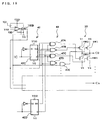
  • FIG. 19 is a circuit chart of a shift register relating to an embodiment of the present invention, and being an improvement of the level shifter of FIG. 9;
  • FIG. 20 is a timing chart for illustrating an operation which does not create instantaneous lighting;
  • FIG. 21 is a circuit chart showing a modification of the level shifter shown in FIG. 19; and
  • FIG. 22 is a circuit chart of another modification of the level shifter shown in FIG. 19.
  • DESCRIPTION OF PREFERRED EMBODIMENT
  • Embodiments of the present invention will be explained with reference to the drawings.
  • 〈Liquid crystal device〉
  • FIG. 1 shows a constitution of major parts of a liquid crystal device, and FIG. 2 is an example of a waveform chart showing a drive waveform for driving the liquid crystal panel of FIG. 1.
  • In FIG. 1, a liquid crystal panel, for example, a simple matrix pattern liquid crystal panel 10, is formed by sealing liquid crystals between a first substrate in which common electrodes CO to Cm are formed, and a second substrate in which segment electrodes S0 to Sn are formed. The point at which one common electrode and one segment electrode cross is a display pixel. The liquid crystal panel 10 has (m + 1) x (n + 1) display pixels.
  • Any other liquid crystal panel such as an active matrix pattern liquid crystal display panel can be used instead of the simple matrix pattern liquid crystal panel 10 in this example.
  • As a drive circuit 20 which drives the liquid crystal panel 10, a common driver 22 connected with the common electrodes C0 to Cm, and a segment driver 24 connected with the segment electrodes S0 to Sn are provided. The common driver 22 and segment driver 24 are supplied with a prescribed voltage from a power supply circuit 30, and selectively supply this prescribed voltage to the common electrodes C0 to Cm or the segment electrodes S0 to Sn in accordance with signals from the drive control circuit 40.
  • FIG. 2 shows an example of a drive waveform during a frame period in which the common electrode C3 in the liquid crystal panel 10 in FIG. 1 is selected.
  • In FIG. 2, the thick solid line indicates the drive waveform supplied to each of the common electrodes C0 to Cm from the common driver 22, whereas the thin solid line indicates the drive waveform supplied to each of the segment electrodes S0 to Sn from the segment driver 24.
  • The polarity of the voltage applied to the liquid crystal in FIG. 2 is inverted from positive to negative, or vice versa, according to the polarity conversion signal FR. For this reason, six levels of drive potential V0 to V5 are used.
  • As shown in FIG. 2, the drive waveform supplied by the common driver 22 varies among the potentials V0, V 1, V4, and V5. On the other hand, the drive waveform supplied by the segment driver 24 varies among the potentials V0, V 2, V3, and V5.
  • 〈Constitution of semiconductor device〉
  • FIG. 3 shows details of a single chip semiconductor device comprising a drive circuit 20, a power supply circuit 30, and a drive control circuit 40 of FIG. 1. The present invention can be applied also to a configuration in which the drive circuit 20, power supply circuit 30, and drive control circuit 40 are mounted on a plurality of chips respectively.
  • In this embodiment of the present invention the first power supply potential to VDD is set VDD = V0. The power supply circuit 30 produces V1 to V5 based on the first power supply potential VDD and the second power supply potential VSS.
  • The power supply circuit 30 has a first logic circuit 31, first to third level shifters 32 to 34, a boosting circuit 35, a constant current circuit 36, a regulator 37, and a voltage follower circuit 38. The constant current circuit 36, regulator 37, and voltage follower circuit 38 function as a bias generating circuit.
  • On the other hand, the drive control circuit 40 has a second logic circuit 41, a fourth level shifter group 42, and a potential selection circuit 43.
  • The first to third level shifters 32 to 34 shift the levels of the logic output I and the inverted output XI of the first logic circuit 31, and the fourth level shifter group 42 shifts the levels of the logic output I and the inverted output XI of the second logic circuit 41.
  • The potential selection circuit 43 in the drive control circuit 40 sends signals to the drive circuit 20 instructing which of the potentials V0 to V5 should be supplied to the common electrode and the segment electrode according to the outputs from the fourth level shifter group 42.
  • In this embodiment, |VDD - VSS| = 3V, for example, VDD = V0 and VSS = -3V. The voltage applied to the liquid crystal
    differs according to the drive duty. For example, if the duty is 1/32, 5V to 7V is required, and if the duty is 1/64, 8V to 12V is required. In either case, the voltage is insufficient if |VDD - VSS| = 3V.
  • Therefore, a boosting circuit 35 and a constant current circuit 36 are provided in the drive circuit 30, to boost |VDD -VSS| = 3V and produce VOUT. In the present embodiment, VOUT = -9V. As shown in FIG. 4, the regulator 37 produces a stable constant potential V5 based on the VOUT. In addition, in the voltage follower circuit 38, the first power supply potential VDD = V0 and the potential V5 from the regulator 37 are divided, for example, into potentials V1 to V4. These operations are schematically shown in FIG. 6.
  • To produce the voltages V1 to V4, the voltage follower circuit 38 has a resistance dividing circuit 38A and first to fourth differential amplifiers 38B to 38E as shown in FIG. 5, for example. A capacitor is provided between the supply line for voltage V0 and each of the supply lines for voltages V1 to V5 and Vout.
  • 〈Cause of instantaneous lighting〉 (Conventional constitution of the fourth level shifter group and the potential selection circuit)
  • Conventional constitutions of the fourth level shifter group 42 and the potential selection circuit 43 shown in FIG. 3 will now be described referring to FIGS. 7 and 8. FIG. 7 shows a constitution of a circuit for supplying voltage to the segment electrodes S0 to Sm of the display part 10, and FIG. 8 shows a constitution of a circuit for supplying voltage to the common electrodes C0 to Cn of the display part 10.
  • In FIG. 7, a level shifter 42A, a potential selection block 43A, and switches SW1, SW4 to SW6 are provided as a voltage supply system for one segment electrode. In addition, a level shifter 42B which is common to the supply system for all segment electrodes is provided in the circuit of FIG. 7. The potential selection block 43A is provided with first to fourth logic gates 44A to 44D which controls turning on and off of the switches SW1 and SW4 to SW6 according to the outputs of the level shifters 42A and 42B.
  • The relationship between the logic of input signal IA (the signal input to the input terminal I of the level shifter 42A) and input signal IB (the signal input to the input terminal I of the level shifter 42B), and the voltage supplied to the segment electrode is shown in Table 1.
    IA H H L L
    IB L H L H
    SEG V5 V0 V3 V2
  • On the other hand, the system supplying voltage to one common electrode shown in FIG. 8 is provided with a level shifter 42C, a potential selection block 43B, and switches SW1 to SW4. A level shifter 42D which is common to the supply system for all common electrodes is also provided in the constitution of FIG. 8. The potential selection block 43B is provided with first to fourth logic gates 45A to 45D which controls turning on and off of the switches SW1 to SW4 according to the outputs of the level shifters 42C and 42D.
  • The relationship between the logic of input signal IC (the signal input to the input terminal I of the level shifter 42C) and input signal ID (the signal input to the input terminal I of the level shifter 42D), and the voltage supplied to the common electrode is shown in Table 2.
    IC H H L L
    ID L H L H
    COM V0 V5 V4 V1
  • (Constitution of each level shifter in the fourth level shifter group)
  • The level shifters 42A to 42D, etc. which constitutes the fourth level shifter group shown in FIG. 3 will now be described referring FIG. 9. As shown in FIG. 9, the level shifters constituting the fourth level shifter group has first and second circuits 55 and 65 connected in parallel to each other. A first P-type MOS transistor 50, a first N-type MOS transistor 51, and a second N-type MOS transistor 52 are connected in series between the supply line of the first power supply potential VDD (= V0) and the supply line of the potential V5, thereby forming a first circuit 55. An output I from the second logic circuit 41 shown in FIG. 2 is supplied to the gate of the first P-type MOS transistor 50 and the gate of the first N-type MOS transistor 51.
  • Parallel to these transistors 50 to 51, a second P-type MOS transistor 60, a third N-type MOS transistor 61, and a fourth N-type MOS transistor 62 are connected in series, whereby a second circuit 65 is formed. An inverted output XI from the second logic circuit 41 shown in FIG. 2 is supplied to the gate of the second P-type MOS transistor 60 and the gate of the third N-type MOS transistor 61.
  • Here, the potential between the first P-type MOS transistor 50 and the first N-type MOS transistor 51 is the inverted output XO of the level shifter 42, and the potential between the second P-type MOS transistor 60 and the third N-type MOS transistor 61 is the output O of the level shifter 42. The inverted output XO is supplied to the gate of the fourth N-type MOS transistor 62, and the output O is supplied to the gate of the second N-type MOS transistor 52.
  • (Operation of the fourth level shifter group)
  • Next, operation of the level shifter group shown in FIG. 9 will be described.
  • Input-output characteristics of the level shifter shown in FIG. 9 are shown in the following Table 3.
    Input I Input XI Output O
    H(VDD) L(VSS) H(VDD)
    L(VSS) H(VDD) L(V5)
    H(VDD) H(VDD) Indefinite
    L(VSS) L(VSS) Indefinite
  • I = XI = H (VDD) or I = XI = L (VSS) in Table 3 indicates the state when the power supply is forcibly shut-off, such as the case where the battery is drawn out. In the case where VDD = OV and VSS = -3V are satisfied, the equation I = XI = VDD = OV is effective when the power supply is forcibly shut-off.
  • Assuming that I = H (VDD) and XI = L (VSS) are satisfied before forcible shut-off of the power supply in the level shifter shown in FIG. 9, what will happen when the power supply is forcibly shut-off will be discussed.
  • In this instance, if the power supply is forcibly shut-off, the input(I) from the second logic circuit 41 will become I = XI = H (VDD), the second P-type MOS transistor 60 turns "off" from "on", and the third N-type MOS transistor 61 turns "on" from "off". Although V5 generated from VOUT shown in FIG. 2 also changes to VDD, this change from V5 to VDD (V5→VDD) is slower than the change from VSS to VDD (VSS →VDD).
  • The reason will be discussed referring to FIG. 10 which shows details of a conventional triple boosting circuit 35.
  • In FIG. 10, an output O of the third level shifter 34 is supplied to the gates of the first and third N- type MOS transistors 81 and 83, and an output XO of the third level shifter 34 is supplied to the gate of the second N-type MOS transistor 82.
  • This boosting circuit 35 has capacitors C1 to C3 which are charged by N to type MOS transistors 81 to 83, of which on/off operation is controlled by the output O and output XO of the third level shifter 34. The output potential VOUT is determined by the amount of the charge provided to the capacitor C3.
  • If the power supply is forcibly shutoff, the capacitor C3 is discharged. The speed of discharge, however, is so slow that discharge will not be completed after the first and the second power supply potentials VDD and VSS become equivalent. Because a potential V5 is generated by a potential VOUT, this potential V5 also does not become equivalent to VDD (= 0V) immediately according to the effect of the charge in the capacitor C3.
  • Here, it is assumed that before forced shut-off of the power supply the input of level shifters 42A, 42B shown in FIG. 7 are IA = IB = H, the input of level shifters 42C, 42D shown in FIG. 8 are IC = H, ID = L, and the segment electrode and common electrode are provided with a potential V0 = VDD as shown in FIG. 18.
  • When the power supply is shut-off, both the inputs I and XI of level shifters 42A to 42D will become HIGH, because there is no logic power supplied to the second logic circuit 41 which is shown in FIG. 3. Thus, the output O of each level shifter 42A to 42D will become indefinite as shown in Table 3. For this reason, the potential V0, which has been selected to be supplied to the segment electrode and common electrode, changes to the other potential (see FIG. 18), whereby the phenomenon of instantaneous lighting occurs in the liquid crystal panel 10 shown in FIG. 1.
  • When the power supply is cut off, the output data V0 from each shift register is refreshed as capacitors are discharged, in the same manner as in the dynamic data holding action in DRAM where data left in the capacitor is held. This is equivalent to the action of dynamically holding data.
  • Specifically, the potential of the output O is decreased to an intermediate level by the on/off operations of the second P-type MOS transistor 60 and the third N-type MOS transistor 61 which are shown in FIG. 9. Finally, the second N-type MOS transistor 52 is turned "off" from "on". The potential of the output XO thus increases.
  • This causes the gate potential of the first to sixth switches (MOS transistor) SW1 to SW6 of the drive circuit 20 shown in FIGS. 7 and 8 to change via the potential selection circuit 43. However, the potential V1 to V5 are not completely discharged due to the effects of the capacitor C2. The above-mentioned instantaneous lighting will occur for these reasons.
  • 〈Countermeasure against instantaneous lighting〉 (Countermeasure against instantaneous lighting in the fourth level shifter group)
  • FIGS. 11 and 12 show segment and common electrode systems in the embodiment of the present invention, in which improved level shifters are used rather than the conventional level shifters shown in FIGS. 7 and 8.
  • In FIGS. 11 and 12, the segment electrode drive system and common electrode drive system are provided with a comparator 100, a reference potential generating circuit 101, and a buffer 102A, all used in common with these drives.
  • A P-type MOS transistor 103 is provided between an input line connected to the input terminal I of the level shifter 42A and a supply line for the first power supply potential VDD, as shown in FIG. 11. In the same manner, a P-type MOS transistor 104 is provided between an input line connected to the input terminal I of the level shifter 42B and a supply line for the first power supply potential VDD, as shown also in FIG. 11.
  • On the other hand, a P-type MOS transistor 105 is provided between an input line connected to the input terminal I of the level shifter 42C and a supply line for the first power supply potential VDD, as shown in FIG. 12. In the same manner, a P-type MOS transistor 106 is provided between an input line connected to the input terminal I of the level shifter 42D and a supply line for the first power supply potential VDD, as shown also in FIG. 12.
  • A reference potential VREG is input to the input terminal of the comparator 100, whereas a second power supply potential VSS is input to the inverted input terminal. The reference potential VREG is produced in the reference potential generating circuit 101 based on the first power supply potential VDD (= OV). VREG is -1.8V, for example. The reference potential generating circuit 101 is made up of one or more N-type MOS transistors which are connected in series and can produce the reference potential VREG by causing the voltage of the first power supply potential VDD to be reduced by the threshold voltage Vth of each transistor.
  • As the output of the comparator 100, HIGH (VDD) is outputted under normal conditions in which the second power supply potential VSS is lower than the reference potential VREG, and LOW (V5) is outputted in the case such as when the power supply is forcibly cut off, in which case the second power supply potential VSS is higher than the reference potential VREG. The output of the buffer 102A is also HIGH (VDD) when the power supply potential is normal, and is LOW (V5) when the power supply potential is abnormal.
  • The comparator 100, reference potential generating circuit 101, and buffer 102A do not necessarily have to be provided in the semiconductor device with the power supply circuit 30 and the like mounted thereon. Instead of using the output from the buffer 102A, it is possible to supply pour-on-reset signals from outside the semiconductor device to the gate of the fourth P-type MOS transistor 63. The power-on-reset signals are detector outputs which always detect potentials of external power supplies and become active when the power supply potential falls below a prescribed value. Therefore, if the power-on-reset signal is LOW active, this is equivalent to the output of the buffer 102A.
  • When the power supply potential is not normal, the output of the buffer 102A becomes LOW (V5) and all four P-type MOS transistors 103 to 106 are turned on, as mentioned above. Therefore, regardless of the logic of signals IA to ID, HIGH (VDD) is inputted in the input terminal I of the level shifters 42A to 42C and LOW (V5) is inputted to the input terminal XI. In addition, LOW (V5) is inputted in the input terminal I of the level shifter 42D and HIGH (VDD) is input to the input terminal XI.
  • Therefore, when the power supply potential is not normal, all switches SW5 to SW6 may set "off", leaving only the switch SW1 "on" by turning only the fourth logic gate 44D "on" in FIG. 11. According to this embodiment the present invention, it is possible to cause the drive circuit 20 to supply the potential V0 (= VDD) to all segment electrodes shown in FIG. 3 by forcibly setting the level shifters 42A and 42B to input (I, XI) = (H, L), when the power supply potential is not normal.
  • In the same manner, when the power supply potential is not normal, all switches SW2 to SW4 may set "off", leaving only the switch SW1 "on" by turning only the fourth logic gate 45A "on" in FIG. 12. According to this embodiment of the present invention, it is possible to cause the drive circuit 20 to supply the potential V0 (= VDD) to all common electrodes shown in FIG. 3 by forcibly setting the level shifter 42D to input (I, XI) = (H, L), when the power supply potential is not normal.
  • Accordingly, when the power supply potential is not normal, malfunctions such as instantaneous lighting of the liquid crystal panel 10 can be prevented by providing all of the segment electrodes and common electrodes with the potential V0 (= VDD = 0V).
  • However, it is preferable that P-type MOS transistors 103 to 106 have a low "ON" resistance (a high capacity).
  • Furthermore, to prevent occurrence of the cases in which two switches among the switches SW1 and SW4 to SW6 in the segment electrode drive system are simultaneously "on" or two switches among the switches SW1 to SW4 in the common electrode drive system are simultaneously "on", it is desirable to provide a period of time during which all switches SW1 to SW6 are turned off.
  • (Countermeasure against instantaneous lighting in the potential selection circuit 43)
  • FIGS. 14 and 15 respectively show a segment electrode drive system and common electrode drive system for a potential selection circuit 43 with which countermeasures against instantaneous lighting is provided.
  • When the power supply is forcibly shut-off, the potential selection circuit 43 turns "on" only the switch SW1 which selects a potential V0 (= VDD), among the switches SW1 to SW6 in the drive circuit 20 shown in FIGS 14 and 15, and outputs signals for turning all other switches SW2 to SW6 "off".
  • The segment electrode drive system shown in FIG. 14 is provided with first to fifth logic gates 46A to 46E which control switches SW1 and SW4 to SW6 on-and-off according to the outputs from the level shifter 42A, 42B, comparator 100, and inversion element 102B.
  • In the sane manner, the common electrode drive system shown in FIG. 15 is provided with first to fifth logic gates 47A to 47E which control switches SW1 to SW4 on-and-off according to the outputs from the level shifter 42A, 42B, comparator 100, and inversion element 102B.
  • When the power supply potential is normal, the output of the comparator 100 is HIGH and the output of the inversion element 102B is LOW. The potential supplied to each segment electrode changes as shown in Table 1 in accordance with the logical state of the input signals IA and IB to the level shifters 42A and 42B.
  • On the other hand, when the power supply potential is not normal, the output of the comparator 100 is LOW and the output of the inversion element 102B is HIGFH. For this reason, the output from the fifth logic gate (AND gate) 46E, to which the output (LOW) from the comparator 100 is input, is LOW regardless of logical states of the input signals IA and IB to the level shifters 42A and 42B, whereby the switch SW1 is turned "on". Switches SW5 to SW6 are turned "off" regardless of logical states of the input signals IA and IB to the level shifters 42A and 42B. All segment electrodes can be supplied with potential V0 (= VDD) by the drive circuit 20 in this manner.
  • When the power supply potential is normal, the output of the comparator 100 is HIGH and the output of the inversion element 102B is LOW also on the common electrode. Therefore, the potential supplied to each segment electrode changes as shown in the above Table 2 according to logic states of input signals IC and ID to the level shifters 42C and 42D.
  • On the other hand, when the power supply potential is not normal, the output of the comparator 100 is LOW and the output of the inversion element 102B is HIGFH. For this reason, the output from the fifth logic gate 47E, to which the output (LOW) from the comparator 100 is input, is LOW regardless of logical states of the input signals IA and IB to the level shifters 42A and 42B, whereby the switch SW1 is turned "on". Switches SW2 to SW4 are turned "off" regardless of the logical states of the input signals IC and ID to the level shifters 42C and 42D. All common electrodes can be supplied with potential V0 (= VDD) by the drive circuit 20 in this manner.
  • Accordingly, when the power supply potential is not normal, malfunctions such as instantaneous lighting of the liquid crystal panel 10 can be prevented by providing all of the segment electrodes and common electrodes with the potential V0 (= VDD = 0V).
  • (Countermeasure against instantaneous lighting in the drive circuit 20)
  • An unproved structured of a final output stage of the drive circuit 20 of FIG. 3 is shown in FIG. 16 and FIG. 17. As shown in FIG. 16 and FIG. 17, all common electrodes C0 to Cn and all segment electrodes S0 to Sm are respectively connected to a P-type MOS transistor 300. In addition, the segment electrode drive system and common electrode drive system shown in FIG. 16 and FIG. 17 are provided with a comparator 100, a reference potential generating circuit 101, and a buffer 102A, all used in common with these drives systems.
  • When the power supply potential is abnormal, the output of the buffer 102A is LOW, causing each P-type MOS transistor 300 to be turned on. This ensures forcible supply of the first power supply potential VDD (= 0V) to all common electrodes C0 to Cn and all segment electrodes S0 to Sm as shown in FIG. 20, even if the output from the level shifter 42 in FIG. 9 becomes indefinite. Malfunctions of instantaneous lighting can be prevented in this manner.
  • In this case, each P-type MOS transistor 300 must have a lower "on"-resistance (higher capacity) than the MOS transistors constituting switches SW1 to SW6. For example, when the "on"-resistance of switches SW1 to SW6 is 1 to 2 K Ω, "on"-resistance of the P-type MOS transistors 103 to 106 should be several tens of Ω.
  • 〈Other countermeasure against instantaneous lighting in the fourth level shifter group〉 (Constitution of each level shifter in the fourth level shifter group)
  • The level shifters 42A to 42D, etc. which constitute the fourth level shifter group shown in FIG. 3 will now be described referring to FIG. 19. As shown in FIG. 19, each of the level shifters constituting the fourth level shifter group 42 has the first and the second circuits 55 and 65 which are connected in parallel to each other. A first P-type MOS transistor 50, a first N-type MOS transistor 51, and a second N-type MOS transistor 52 are connected in series between the supply line for the first power supply potential VDD (= V0) and the supply line for the potential V5, thereby forming a first circuit 55. An output I from the second logic circuit 41 shown in FIG. 2 is supplied to the gate of the first P-type MOS transistor 50 and the gate of the first N-type MOS transistor 51.
  • Parallel to these transistors 50 to 51, a second P-type MOS transistor 60, a third N-type MOS transistor 61, and a fourth N-type MOS transistor 62 are connected in series, whereby a second circuit 65 is formed. An inverted output XI from the second logic circuit 41 shown in FIG. 2 is supplied to the gate of the second P-type MOS transistor 60 and the gate of the third N-type MOS transistor 61.
  • Here, the potential between the first P-type MOS transistor 50 and the first N-type MOS transistor 51 is the inverted output XO of the level shifter 42, and the potential between the second P-type MOS transistor 60 and the third N-type MOS transistor 61 is the output O of the level shifter 42. The inverted output XO is supplied to the gate of the fourth N-type MOS transistor 62, and the output O is supplied to the gate of the second N-type MOS transistor 52.
  • In this embodiment, a third P-type MOS transistor 53 is provided parallel to the first P-type MOS transistor 50, and a fourth P-type MOS transistor 63 is provided parallel to the second P-type MOS transistor 60. The inverted output XO is supplied to the gate of the fourth P-type MOS transistor 63, and the output O is supplied to the gate of the third P-type MOS transistor 53.
  • (Operation of the fourth level shifter group)
  • The operation of the level shifter in this embodiment of the present invention shown in FIG. 19 will now be described, comparing with the operation of a conventional level shifter shown in FIG. 9 which does not have the third and fourth P- type MOS transistors 53 and 63.
  • In the conventional level shifter shown in FIG. 9, when an input of I = XI = OV = HIGH is established by turning the power supply off, the potential of the output O decreases to an intermediate level by the on/off operations of the second P-type MOS transistor 60 and the third N-type MOS transistor 61, finally causing the second N-type MOS transistor 52 to be turned "off" from "on". The potential of the output XO thus increases, causing the output to be indefinite. This results in instantaneous lighting.
  • In contrast, when the level shifter in this embodiment shown in FIG. 19 is applied to the first to third level shifters 42A to 42C, the relationship IA = IB = IC = HIGH is established by a power saving command and reset before cut-off of the power supply, and the level shifter inputs in FIG. 19 are I = HIGH and XI = LOW. In this instance, the outputs of the level shifter are O = VDD = HIGH and XO = V5 = LOW.
  • When the relationship I = XI = HIGH is established by a power supply shut-off after this, the second P-type MOS transistor 60 changes from "on" to "off". However, the fourth P-type MOS transistor 63, which is connected in parallel with the second P-type MOS transistor 60, continues to be "on" because the gate is charged with the potential of the output XO = V5. Therefore the output O remains as output O = VDD. If the output O = VDD is maintained, the first and third P- type MOS transistors 50, 53 are turned "off" because of the relationship of the input I = H (VDD), thereby turning the first and the second N- type MOS transistors 51 and 52 "on". An inverted output XO = V5 can thus be maintained.
  • In this manner, even if the input from the second logic circuit 41 is I = XI = H (VDD) in the event of a power supply shut-off, the outputs (O, XO) of the level shifters 42A to 42C in the fourth level shifter group 42 in the embodiment shown in FIG. 19 can be set to the output conditions (VDD, V5) which were effective before the power supply shut-off. Thus, the output will not become indefinite as in the case of the conventional level shifters shown in FIG. 9.
  • Accordingly, in the level shifters 42A to 42C shown in FIG. 7 and FIG. 8, when the input is I = XI = HIGH, the output is O = VDD = HIGH, XO = V5 = LOW. Thus, the state before power supply shut-off can be maintained.
  • In the level shifter 42D shown in FIG. 8, the input and output of the level shifter shown in FIG. 19 before shut-off the power supply are respectively I = LOW, XI = HIGH and O = V5 = LOW, XO = VDD = HIGH. When the power supply is disconnected after this, even if the first P-type MOS transistor 50 in FIG. 19 is turned "off" from "on", the third P-type MOS transistor 53 which is connected parallel to this transistor 50 continues to be "on" because the gate is charged with a potential of the output O = V5. Thus, the output XO can be maintained at XO = VDD. When the output XO = VDD is maintained, both the second and fourth P- type MOS transistors 50, 53 continue to be "off" because of the relationship of the input XI = H (VDD), thereby holding the third and fourth N- type MOS transistors 61 and 62 "on". An output XO = V5 can thus be maintained.
  • In this manner, ever after a shutoff of the power supply the third and fourth level shifters 42C and 42D in FIG. 8 can maintain the same output conditions as those which existed before the shut-off. Therefore, each level shifter 42A to 42D in FIG. 7 and FIG. 8 can be operated in a normal manner to continue supply of potential V0 to all common and segment electrodes as shown in FIG. 20. Instantaneous lighting can thus be prevented.
  • (Modification of level shifter)
  • FIG. 21 and FIG. 22 are modified examples of the level shifter provided with measures for preventing malfunctions due to instantaneous lighting.
  • In FIG. 21, a fourth P-type MOS transistor 63 is provided being connected parallel with the second P-type MOS transistor 60, but the third P-type MOS transistor 53 is not provided. In FIG. 22, on the other hand, a third P-type MOS transistor 53 is provided being connected parallel with the first P-type MOS transistor 50, but the fourth P-type MOS transistor 63 is not provided.
  • The gate of the fourth P-type MOS transistor 63 in FIG. 21 and the gate of the third P-type MOS transistor 53 in FIG. 22 are supplied with the output of the comparator 100 which was described in the above described embodiment. Because the output of the comparator 100 is the same as that shown in FIG. 13, the fourth P-type MOS transistor 63 in FIG. 21 and the third P-type MOS transistor 53 in FIG. 22 are turned "on" at the time of a power supply emergency.
  • The level shifter of the present embodiment shown in FIG. 21 can be applied to the first to third level shifters 42A to 42C in FIGS. 7 and 8. Because the relationship of IA = IB = IC = HIGH was effective among the level shifters 42A to 42C before the power supply shut-off, the level shifter inputs are I = HIGH and XI = LOW in FIG. 21. In this instance, the outputs of the level shifter are O = VDD = HIGH and XO = V5 = LOW.
  • When the relationship I = XI = HIGH is established by a power supply shut-off after this, the second P-type MOS transistor 60 changes from "on" to "off". However, the fourth P-type MOS transistor 63 which is connected in parallel with the second P-type MOS transistor 60 is turned "on" at the time of the power supply emergency by the LOW signal from the comparator 100. The output O = VDD can be maintained in this manner. When the output XO = V5 is maintained, both the first and third P- type MOS transistors 50, 53 are turned "off" because of the relationship of the input I = H (VDD), thereby turning the first and the second N- type MOS transistors 51 and 52 "on". An inverted output XO = V5 can thus be maintained.
  • Therefore, even if the level shifter of FIG. 21 is applied to the first to third level shifters 42A to 42C in FIGS 7 and 8, the same results as the results obtained using the level shifter shown in FIG. 19 can be obtained.
  • On the other hand, if the level shifter shown in FIG. 22 is applied to the level shifter shown in FIG.8, the input of the level shifter shown in FIG. 22 before shut off the power supply is I = LOW, XI = HIGH and the output is O = V5 = LOW, XO = VDD = HIGH. When the power supply is disconnected after this, even if the first P-type MOS transistor 50 in FIG. 22 is turned "off" from "on", the third P-type MOS transistor 53 which is connected in parallel with this transistor 50 is maintained "on" due to the output of the comparator 100 at the time of the power supply emergency. Thus, the output XO can be maintained at XO = VDD. When the output XO = VDD is maintained, both the second and fourth P- type MOS transistors 50, 53 are turned "off" because of the relationship of the input XI = H (VDD), thereby holding the third and fourth N- type MOS transistors 61 and 62 to be "on". An output XO = V5 can thus be maintained.
  • Therefore, even if the level shifter of FIG. 22 is applied to the level shifter 42D in FIG 8, the same results as the results obtained using the level shifter shown in FIG. 19 can be obtained.
  • The present invention is not limited to the embodiments described above, and many modifications and variations are possible without departing from the spirit and scope of the present invention.
  • For example, it is needless to mention that the second power supply potential which was a negative potential in the embodiments described above may be a positive potential.
  • The present invention can be applied to various types of electronic equipment such as cellular phones, game machines, electronic pocketbooks, personal computers, word processor equipment, navigation devices, and the like on which the liquid crystal panel 10 shown in FIG. 1 is mounted.

Claims (15)

  1. A semiconductor device including a drive circuit, a drive control circuit which controls the drive circuit, and a power supply circuit which supplies a potential to the drive circuit and drive control circuit,
    wherein the power supply circuit comprises:
    a boosting circuit, to which a first power supply potential which is a ground potential from an external power supply and a second power supply potential which is a potential other than the ground potential are supplied, and raising the absolute value of the second power supply potential and charging the boosted potential to the capacitor; and
    a bias generating circuit generating a potential supplied to the drive circuit and the drive control circuit based on the output potential of the boosting circuit, and
    wherein the first power supply potential and a potential from the bias generating circuit are supplied to the drive circuit that outputs a potential selected from potentials supplied in accordance with a control of the drive control circuit during a normal power supply period, and, in the event of a power supply emergency in which an absolute value between the first and the second power supply potentials is lower than a given value, changes all potentials outputted from the drive circuit into the first power supply potential based on the signal activated in the event of the power supply emergency.
  2. The semiconductor device according to claim 1, further comprising a comparator which compares a reference potential having an absolute value smaller than the absolute value between the first and the second power supply potentials, with the second power supply potential, so that a signal activated in the event of the power supply emergency is outputted.
  3. The semiconductor device according to claim 1,
    wherein the signal activated in the event of the power supply emergency is a power-on-reset signal which is supplied from outside the semiconductor device.
  4. A semiconductor device including a drive circuit, a drive control circuit which controls the drive circuit, and a power supply circuit which supplies a potential to the drive circuit and drive control circuit,
    wherein the power supply circuit comprises:
    a boosting circuit, to which a first power supply potential which is a ground potential from an external power supply and a second power supply potential which is a potential other than the ground potential are supplied, and raising the absolute value of the second power supply potential and charging the boosted potential to the capacitor; and
    a bias generating circuit generating a potential supplied to the drive circuit and the drive control circuit based on the output potential of the boosting circuit,
    wherein the first power supply potential and a potential from the bias generating circuit are supplied to the drive circuit that outputs a potential selected from potentials supplied in accordance with a control of the drive control circuit, and
    wherein in the event of a power supply emergency in which an absolute value between the first and the second power supply potentials is lower than a specified value, the drive control circuit outputs a potential selecting signal that changes all potentials outputted from the drive circuit into the first power supply potential based on the signal activated when the power supply emergency occurs.
  5. The semiconductor device according to claim 4,
    wherein the drive control circuit comprises:
    a logic circuit to which the first and the second power supply potentials are supplied, and outputting various logic levels;
    a level shifter group to which a potential from the power supply circuit and the first power supply potential are supplied, including a plurality of level shifters for shifting the logic levels from the logic circuit; and
    a potential selection circuit for outputting potential selection signals supplied to the drive circuit based on the output from the level shifter group.
  6. The semiconductor device according to claim 5,
    wherein the level shifter group has an input level setting circuit for setting the input to the level shifters at a specified value based on the signals which become active in the event of a power supply emergency regardless of the output of the logic circuit.
  7. The semiconductor device according to claim 5,
    wherein the potential selection circuit has an output level setting circuit for setting the output of the potential selection circuit at a specified value based on the signals which become active in the event of a power supply emergency regardless of the output of the level shifter group.
  8. The semiconductor device according to any one of claims 4 to 7, further comprising a comparator which compares a reference potential having an absolute value smaller than the absolute value between the first and the second power supply potentials, with the second power supply potential, so that a signal activated in the event of the power supply emergency is outputted.
  9. The semiconductor device according to any one of claims 4 to 7,
    wherein the signal activated in the event of the power supply emergency is a power-on-reset signal which is supplied from outside the semiconductor device.
  10. A semiconductor device including a drive circuit, a drive control circuit which controls the drive circuit, and a power supply circuit which supplies a potential to the drive circuit and drive control circuit,
    wherein the power supply circuit comprises:
    a boosting circuit, to which a first power supply potential which is a ground potential from an external power supply and a second power supply potential which is a potential other than the ground potential are supplied, and raising the absolute value of the second power supply potential and charging the boosted potential to the capacitor; and
    a bias generating circuit generating a potential supplied to the drive circuit and the drive control circuit based on the output potential of the boosting circuit, and
    wherein the first power supply potential and a potential from the bias generating circuit are supplied to the drive circuit that outputs a potential selected from potentials supplied in accordance with a control of the drive control circuit during a normal power supply period, and
    wherein the drive control circuit comprises:
    a logic circuit to which the first and the second power supply potentials are supplied, and outputting a first logic level and a second logic level;
    a level shifter group to which a potential from the power supply circuit and the first power supply potential are supplied, and shifting an output level from the logic circuit; and
    a potential selection circuit for outputting potential selection signals supplied to the drive circuit based on the output from the level shifter group,
    wherein:
    each of level shifters forming the level shifter group comprises first and second circuits which are connected in parallel between a supply line for the first power supply potential and a supply line for a potential supplied by the power supply circuit;
    the first circuit includes a first MOS transistor of primary conductive-type, a first MOS transistor of secondary conductive-type, and a second MOS transistor of secondary conductive-type which are connected in series to the first circuit, the first logic level from the logic circuit is supplied to gates of the first MOS transistor of primary conductive-type and the first MOS transistor of secondary conductive-type, and a potential between the first MOS transistor of primary conductive-type and the first MOS transistor of secondary conductive-type is a first output potential of each of the level shifters;
    the second circuit includes a second MOS transistor of primary conductive-type, a third MOS transistor of secondary conductive-type, and a forth MOS transistor of secondary conductive-type which are connected in series to the second circuit, the second logic level from the logic circuit is supplied to gates of the second MOS transistor of primary conductive-type and the third MOS transistor of secondary conductive-type, and a potential between the second MOS transistor of primary conductive-type and the third MOS transistor of secondary conductive-type is a second output potential of each of the level shifters;
    the second output potential is supplied to a gate of the second MOS transistor of secondary conductive-type in the first circuit, and the first output potential is supplied to a gate of the forth MOS transistor of secondary conductive-type; and
    each of the level shifters further includes a potential maintaining circuit for maintaining the first and the second output potentials of each of the level shifters at a state before occurrence of a power supply emergency, in the event of a power supply emergency in which an absolute value between the first and the second power supply potentials is lower than a prescribed value.
  11. The semiconductor device according to claim 10,
    wherein the potential maintaining circuit provided in each of the level shifters forming the level shifter group comprises:
    a third MOS transistor of primary conductive-type connected in parallel with the first MOS transistor of primary conductive-type; and
    a forth MOS transistor of primary conductive-type connected in parallel with the second MOS transistor of primary conductive-type, and
    wherein the second output potential is supplied to a gate of the third MOS transistor of primary conductive-type, and the first output potential is supplied to a gate of the fourth MOS transistor of primary conductive-type.
  12. The semiconductor device according to claim 10,
    wherein the potential maintaining circuit provided in at least one of the level shifters forming the level shifter group includes a third MOS transistor of primary conductive-type connected in parallel to the first MOS transistor of primary conductive-type, and, when an on/off state of the first MOS transistor of primary conductive-type changes before and after the power supply emergency, the on/off state of the third MOS transistor of primary conductive-type is set identical to an on/off state of the first MOS transistor of primary conductive-type which existed before the power supply emergency.
  13. The semiconductor device according to claim 10,
    wherein the potential maintaining circuit provided in at least one of the level shifters forming the level shifter group includes a fourth MOS transistor of primary conductive-type connected in parallel to the second MOS transistor of primary conductive-type, and, when an on/off state of the second MOS transistor of primary conductive-type changes before and after the power supply emergency, the on/off state of the fourth MOS transistor of primary conductive-type after the power supply emergency is set identical to an on/off state of the second MOS transistor of primary conductive-type before the power supply emergency.
  14. A liquid crystal device comprising the semiconductor device as defined in any one of claims 1 to 13, and a liquid crystal panel being driven based on the voltage supplied by the semiconductor device.
  15. Electronic equipment comprising the liquid crystal device as defined in claim 14.
EP00106090A 1999-03-30 2000-03-30 Semiconductor device including a power supply, and liquid crystal device and electronic equipment using the same Withdrawn EP1041533A1 (en)

Applications Claiming Priority (4)

Application Number Priority Date Filing Date Title
JP8966799 1999-03-30
JP2000006416 2000-01-14
JP2000006416A JP3584830B2 (en) 1999-03-30 2000-01-14 Semiconductor device and liquid crystal device and electronic equipment using the same

Publications (1)

Publication Number Publication Date
EP1041533A1 true EP1041533A1 (en) 2000-10-04

Family

ID=26431084

Family Applications (1)

Application Number Title Priority Date Filing Date
EP00106090A Withdrawn EP1041533A1 (en) 1999-03-30 2000-03-30 Semiconductor device including a power supply, and liquid crystal device and electronic equipment using the same

Country Status (3)

Country Link
US (2) US6300797B1 (en)
EP (1) EP1041533A1 (en)
JP (1) JP3584830B2 (en)

Cited By (2)

* Cited by examiner, † Cited by third party
Publication number Priority date Publication date Assignee Title
WO2002054374A1 (en) * 2000-12-28 2002-07-11 Koninklijke Philips Electronics N.V. A liquid crystal display device with afterimage reduction when power is turned off
WO2005004100A1 (en) * 2003-07-03 2005-01-13 Arcelik Anonim Sirketi A control card and a control method for domestic appliances

Families Citing this family (13)

* Cited by examiner, † Cited by third party
Publication number Priority date Publication date Assignee Title
JP3584830B2 (en) * 1999-03-30 2004-11-04 セイコーエプソン株式会社 Semiconductor device and liquid crystal device and electronic equipment using the same
TW591268B (en) * 2001-03-27 2004-06-11 Sanyo Electric Co Active matrix type display device
ITMI20021424A1 (en) * 2002-06-27 2003-12-29 St Microelectronics Srl DEVICE FOR PILOTING COLUMNS OF A LIQUID CRYSTAL DISPLAY
US6982587B2 (en) * 2002-07-12 2006-01-03 Rambus Inc. Equalizing transceiver with reduced parasitic capacitance
US6873503B2 (en) * 2002-09-19 2005-03-29 Sun Microsystems, Inc. SSTL pull-up pre-driver design using regulated power supply
JP4907908B2 (en) * 2005-06-29 2012-04-04 ルネサスエレクトロニクス株式会社 Driving circuit and display device
JP4407670B2 (en) * 2006-05-26 2010-02-03 セイコーエプソン株式会社 Electro-optical device and electronic apparatus
KR100833755B1 (en) * 2007-01-15 2008-05-29 삼성에스디아이 주식회사 Onejang test device and method thereof
JP5786294B2 (en) * 2010-08-31 2015-09-30 セイコーエプソン株式会社 Integrated circuit device and electronic apparatus
JP5937853B2 (en) * 2012-03-09 2016-06-22 ローム株式会社 Gamma correction voltage generation circuit and electronic device including the same
JP6378003B2 (en) * 2014-08-27 2018-08-22 ラピスセミコンダクタ株式会社 Semiconductor device, battery monitoring system, and semiconductor device startup method
TWI540559B (en) * 2015-05-28 2016-07-01 矽創電子股份有限公司 Source driving circuit
JP2018109705A (en) 2017-01-05 2018-07-12 三菱電機株式会社 Driver IC and liquid crystal display device

Citations (11)

* Cited by examiner, † Cited by third party
Publication number Priority date Publication date Assignee Title
JPS63316896A (en) * 1987-06-19 1988-12-26 セイコーエプソン株式会社 Liquid crystal driving circuit
EP0424958A2 (en) * 1989-10-27 1991-05-02 Canon Kabushiki Kaisha Liquid crystal display apparatus having controlled power-off
EP0479304A2 (en) * 1990-10-05 1992-04-08 Kabushiki Kaisha Toshiba Power source apparatus for driving liquid crystal display
EP0642112A1 (en) * 1993-09-03 1995-03-08 Oki Electric Industry Co., Ltd. Drive voltage generating circuit having a contrast control function
JPH08146379A (en) * 1994-11-25 1996-06-07 Hitachi Ltd Liquid crystal driving circuit
EP0721137A1 (en) * 1994-07-14 1996-07-10 Seiko Epson Corporation Power source circuit, liquid crystal display device, and electronic device
US5745092A (en) * 1993-12-22 1998-04-28 Seiko Epson Corporation Liquid-Crystal display system and power supply method that supply different logic source voltages to signal and scan drivers
JPH10214067A (en) * 1996-11-26 1998-08-11 Sharp Corp Erasing device of liquid crystal display picture and liquid crystal display device which is provided with the erasing device
JPH10214063A (en) * 1997-01-30 1998-08-11 Hitachi Ltd Liquid crystal display controller and liquid crystal display device
EP0881622A1 (en) * 1997-05-27 1998-12-02 International Business Machines Corporation Power-off screen clearing circuit for active matrix liquid crystal display
JPH1114961A (en) * 1997-04-28 1999-01-22 Toshiba Microelectron Corp Liquid crystal driving circuit

Family Cites Families (3)

* Cited by examiner, † Cited by third party
Publication number Priority date Publication date Assignee Title
DE69023751T2 (en) * 1989-05-26 1996-06-20 Seiko Epson Corp POWER SOURCE SWITCHING.
KR0172373B1 (en) * 1995-09-14 1999-03-30 김광호 Data output buffer in semiconductor
JP3584830B2 (en) * 1999-03-30 2004-11-04 セイコーエプソン株式会社 Semiconductor device and liquid crystal device and electronic equipment using the same

Patent Citations (14)

* Cited by examiner, † Cited by third party
Publication number Priority date Publication date Assignee Title
JPS63316896A (en) * 1987-06-19 1988-12-26 セイコーエプソン株式会社 Liquid crystal driving circuit
EP0424958A2 (en) * 1989-10-27 1991-05-02 Canon Kabushiki Kaisha Liquid crystal display apparatus having controlled power-off
EP0479304A2 (en) * 1990-10-05 1992-04-08 Kabushiki Kaisha Toshiba Power source apparatus for driving liquid crystal display
EP0642112A1 (en) * 1993-09-03 1995-03-08 Oki Electric Industry Co., Ltd. Drive voltage generating circuit having a contrast control function
US5745092A (en) * 1993-12-22 1998-04-28 Seiko Epson Corporation Liquid-Crystal display system and power supply method that supply different logic source voltages to signal and scan drivers
EP0721137A1 (en) * 1994-07-14 1996-07-10 Seiko Epson Corporation Power source circuit, liquid crystal display device, and electronic device
JPH08146379A (en) * 1994-11-25 1996-06-07 Hitachi Ltd Liquid crystal driving circuit
JPH10214067A (en) * 1996-11-26 1998-08-11 Sharp Corp Erasing device of liquid crystal display picture and liquid crystal display device which is provided with the erasing device
US6151016A (en) * 1996-11-26 2000-11-21 Sharp Kabushiki Kaisha Erasing device for liquid crystal display image and liquid crystal display device including the same
JPH10214063A (en) * 1997-01-30 1998-08-11 Hitachi Ltd Liquid crystal display controller and liquid crystal display device
US6181313B1 (en) * 1997-01-30 2001-01-30 Hitachi, Ltd. Liquid crystal display controller and liquid crystal display device
JPH1114961A (en) * 1997-04-28 1999-01-22 Toshiba Microelectron Corp Liquid crystal driving circuit
US6166726A (en) * 1997-04-28 2000-12-26 Kabushiki Kaisha Toshiba Circuit for driving a liquid crystal display
EP0881622A1 (en) * 1997-05-27 1998-12-02 International Business Machines Corporation Power-off screen clearing circuit for active matrix liquid crystal display

Cited By (3)

* Cited by examiner, † Cited by third party
Publication number Priority date Publication date Assignee Title
WO2002054374A1 (en) * 2000-12-28 2002-07-11 Koninklijke Philips Electronics N.V. A liquid crystal display device with afterimage reduction when power is turned off
US6690345B2 (en) 2000-12-28 2004-02-10 Koninklijke Philips Electronics N.V. Liquid crystal display device
WO2005004100A1 (en) * 2003-07-03 2005-01-13 Arcelik Anonim Sirketi A control card and a control method for domestic appliances

Also Published As

Publication number Publication date
JP3584830B2 (en) 2004-11-04
US6525567B2 (en) 2003-02-25
US20010048322A1 (en) 2001-12-06
US6300797B1 (en) 2001-10-09
JP2000347614A (en) 2000-12-15

Similar Documents

Publication Publication Date Title
US10978114B2 (en) Shift register unit, gate driving circuit, display device and driving method to reduce noise
US6911964B2 (en) Frame buffer pixel circuit for liquid crystal display
EP1041533A1 (en) Semiconductor device including a power supply, and liquid crystal device and electronic equipment using the same
JP3428380B2 (en) Semiconductor device for drive control of liquid crystal display device and liquid crystal display device
US8754838B2 (en) Discharge circuit and display device with the same
US6917236B2 (en) Method and apparatus for level shifting
JP2006201760A (en) Driver circuit of display device and method of driving the same
US20080186266A1 (en) Display driver ic having embedded memory
US20210256927A1 (en) Circuit and method for preventing screen flickering, drive circuit for display panel, and display apparatus
US7084851B2 (en) Display device having SRAM built in pixel
JP4204204B2 (en) Active matrix display device
KR100459624B1 (en) Display device
KR100481108B1 (en) Display apparatus and driving method thereof
JPH07235844A (en) Output buffer circuit for analog driver ic
JP3799869B2 (en) Semiconductor device equipped with power supply circuit, and liquid crystal device and electronic device using the same
US7138993B2 (en) LCD with integrated switches for DC restore
KR100522060B1 (en) Display device
US10783818B2 (en) Dual gate transistor circuit, pixel circuit and gate drive circuit thereof
US7330171B2 (en) Amplifier circuit
JP4278314B2 (en) Active matrix display device
JP2006163222A (en) Electrooptical apparatus and electronic equipment
JP4197852B2 (en) Active matrix display device
CN216487245U (en) Shift register, grid drive circuit and display panel
JP4297629B2 (en) Active matrix display device
JP4297628B2 (en) Active matrix display device

Legal Events

Date Code Title Description
PUAI Public reference made under article 153(3) epc to a published international application that has entered the european phase

Free format text: ORIGINAL CODE: 0009012

AK Designated contracting states

Kind code of ref document: A1

Designated state(s): AT BE CH CY DE DK ES FI FR GB GR IE IT LI LU MC NL PT SE

AX Request for extension of the european patent

Free format text: AL;LT;LV;MK;RO;SI

17P Request for examination filed

Effective date: 20010302

AKX Designation fees paid

Free format text: AT BE CH CY DE DK ES FI FR GB GR IE IT LI LU MC NL PT SE

17Q First examination report despatched

Effective date: 20071002

STAA Information on the status of an ep patent application or granted ep patent

Free format text: STATUS: THE APPLICATION IS DEEMED TO BE WITHDRAWN

18D Application deemed to be withdrawn

Effective date: 20100407