EP1041444A2 - Vorrichtung und Verfahren zur Herstellung einer Halbleitervorrichtung - Google Patents
Vorrichtung und Verfahren zur Herstellung einer Halbleitervorrichtung Download PDFInfo
- Publication number
- EP1041444A2 EP1041444A2 EP00400922A EP00400922A EP1041444A2 EP 1041444 A2 EP1041444 A2 EP 1041444A2 EP 00400922 A EP00400922 A EP 00400922A EP 00400922 A EP00400922 A EP 00400922A EP 1041444 A2 EP1041444 A2 EP 1041444A2
- Authority
- EP
- European Patent Office
- Prior art keywords
- light
- wavelength
- laser
- wafer
- semiconductor device
- Prior art date
- Legal status (The legal status is an assumption and is not a legal conclusion. Google has not performed a legal analysis and makes no representation as to the accuracy of the status listed.)
- Withdrawn
Links
Images

Classifications
-
- H—ELECTRICITY
- H01—ELECTRIC ELEMENTS
- H01L—SEMICONDUCTOR DEVICES NOT COVERED BY CLASS H10
- H01L21/00—Processes or apparatus adapted for the manufacture or treatment of semiconductor or solid state devices or of parts thereof
- H01L21/02—Manufacture or treatment of semiconductor devices or of parts thereof
- H01L21/027—Making masks on semiconductor bodies for further photolithographic processing not provided for in group H01L21/18 or H01L21/34
-
- G—PHYSICS
- G03—PHOTOGRAPHY; CINEMATOGRAPHY; ANALOGOUS TECHNIQUES USING WAVES OTHER THAN OPTICAL WAVES; ELECTROGRAPHY; HOLOGRAPHY
- G03F—PHOTOMECHANICAL PRODUCTION OF TEXTURED OR PATTERNED SURFACES, e.g. FOR PRINTING, FOR PROCESSING OF SEMICONDUCTOR DEVICES; MATERIALS THEREFOR; ORIGINALS THEREFOR; APPARATUS SPECIALLY ADAPTED THEREFOR
- G03F7/00—Photomechanical, e.g. photolithographic, production of textured or patterned surfaces, e.g. printing surfaces; Materials therefor, e.g. comprising photoresists; Apparatus specially adapted therefor
- G03F7/70—Microphotolithographic exposure; Apparatus therefor
- G03F7/70008—Production of exposure light, i.e. light sources
Definitions
- the present invention relates to a semiconductor manufacturing apparatus and a semiconductor device manufacturing method, more particularly a semiconductor manufacturing apparatus emitting light having a high brightness, high energy, and short pulse width for ablation to form a pattern on a wafer and a semiconductor device manufacturing method using the apparatus.
- the method is also known emitting light using a high-brightness light source and sublimating the material to form a pattern (ablation).
- ablation the inner-shell electrons of various materials participate in a photochemical reaction to form a pattern to a high precision.
- a pattern can be formed by ablation, specifically the organic material polymethyl methacrylate (R. Srinivasan and Bodil Braren, Applied Physics Letters, 1988, 53, 1233) and Teflon (S. Kuper and M. Stuke, Applied Physics Letters, 1989, 54, 4), the inorganic material SiO2, and the semiconductor material GaAs can be mentioned.
- a processing device using ablation to be able to form a pattern on for example a polyimide film is disclosed by Japanese Unexamined Patent Publication (Kokai) No. 8-155667.
- This processing device emits a laser beam having a pulse width of about 20 ns, for example, to process a material.
- a method and apparatus using ablation to form a signal groove (pit) on an optical disk comprised of a synthetic resin are disclosed in Japanese Unexamined Patent Publication (Kokai) No. 8-124226. According to this method of production of an optical disk, it is possible to use a fourth harmonic (266 nm wavelength) of for example an Nd:YAG laser to form a pit (currently 0.4 ⁇ m in width).
- a method of production of a liquid-crystal display element using ablation to form a pattern on thin film layers of liquid-crystal display elements is disclosed in Japanese Unexamined Patent Publication (Kokai) No. 8-6070.
- a pattern is formed by using an excimer laser of an ultraviolet region such as a KrF laser (248 nm wavelength), a XeCl excimer laser (308 nm wavelength), or an ArF excimer laser (193 nm wavelength).
- the pulse width of these lasers is about 10 to 100 ns.
- An object of the present invention is to provide a semiconductor manufacturing apparatus and a method of producing a semiconductor device able to form a sufficiently precise pattern by ablation.
- the semiconductor manufacturing apparatus of the present invention is a semiconductor manufacturing apparatus comprising a light source for emitting light of a first wavelength on a surface of a wafer and a mask through which at least part of the light of the first wavelength passes and removing a material of the part of the wafer exposed by the light of the first wavelength by vaporization, characterized in that the light source comprises an electron beam generating mean for generating an electron beam and a light emitting means for emitting light of a second wavelength longer than the first wavelength and in that the light of the first wavelength is an inverse Compton scattered light obtained by collision of electrons in the electron beam with photons in the light of the second wavelength causing the energy of the electrons to be given to the photons.
- the semiconductor manufacturing apparatus of the present invention preferably is characterized in that the light emitting means comprises a laser.
- the semiconductor manufacturing apparatus of the present invention more preferably is characterized in that the laser comprises a pulsed laser.
- the semiconductor manufacturing apparatus of the present invention preferably is characterized in that the light source has at least a pair of reflecting means for reflecting the light of the second wavelength back and forth.
- the semiconductor manufacturing apparatus of the present invention is a semiconductor manufacturing apparatus comprising a light source for emitting a pulsed light to a surface of a wafer and a mask through which at least a part of the pulsed light passes and removing a material of the part of the wafer exposed by the pulsed light by vaporization, characterized in that the pulsed light emitted from the light source has a wavelength of not more than about 300 nm and a pulse width of not more than about 1 ns.
- the semiconductor manufacturing apparatus of the present invention preferably is characterized in that the light source comprises a light source emitting a synchrotron radiation light.
- the semiconductor manufacturing apparatus of the present invention preferably is characterized in that the light source emits a laser plasma light.
- the semiconductor device manufacturing method of the present invention is characterized by comprising the steps of generating light of a first wavelength; emitting the light of the first wavelength to the surface of a wafer via a mask through which at least part of the light of the first wavelength passes; and removing material of a part of a wafer exposed by the light of the first wavelength by vaporization, wherein the step of generating the light of the first wavelength comprises the steps of generating an electron beam from an electron beam generating mean; generating light of a second wavelength longer than the first wavelength; and making electrons in the electron beam collide with photons in the light of the second wavelength to generate inverse Compton scattered light with the energy of the electrons given to the photons.
- the semiconductor device manufacturing method of the present invention preferably is characterized in that the light of the second wavelength comprises a laser light.
- the semiconductor device manufacturing method of the present invention more preferably is characterized in that the laser light comprises a pulsed light.
- the semiconductor device manufacturing method of the present invention preferably is characterized in that the step of generating the light of the first wavelength comprises a step of using at least a pair of reflecting means to reflect the light of the second wavelength back and forth to make the electrons collide with the photons.
- the semiconductor device manufacturing method of the present invention preferably is characterized in that a dielectric layer is formed on the surface of the wafer.
- the semiconductor device manufacturing method of the present invention preferably is characterized in that a semiconductor layer is formed on the surface of the wafer.
- the semiconductor device manufacturing method of the present invention preferably is characterized in that a metal layer is formed on the surface of the wafer.
- the semiconductor device manufacturing method of the present invention is characterized by comprising the steps of emitting a pulsed light of predetermined wavelength to a surface of a wafer via a mask through which at least a part of the pulsed light passes and removing a material of the part of the wafer exposed by the pulsed light by vaporization, wherein the pulsed light has a wavelength of not more than about 300 nm and a pulse width of not more than about 1 ns.
- the semiconductor device manufacturing method of the present invention preferably is characterized in that the pulsed light is a synchrotron radiation light.
- the semiconductor device manufacturing method of the present invention preferably is characterized in that the pulsed light comprises a laser plasma light.
- the semiconductor device manufacturing method of the present invention unlike the case of conventional etching, a series of steps such as exposure and development of a resist and etching using the resist as a mask becomes unnecessary.
- a series of steps such as exposure and development of a resist and etching using the resist as a mask becomes unnecessary.
- the material of the light-exposed part can be removed, so it is made possible to simplify the process of production.
- the semiconductor device manufacturing method of the present invention when forming a resist on the surface of the wafer and emitting light there, it is also possible to continuously pattern the resist and pattern a base wafer material.
- a vaporization reaction of a material by light irradiation is used to remove the material of an exposed part and form a pattern on the surface.
- ablation light irradiation
- the energy of photons (wavelength) and the number of photons can be mentioned.
- the former photon energy is important for exciting the inner-shell electrons.
- a shorter wavelength is preferable.
- a material of the surface to be processed is an organic material such as an acrylic resin or a fluororesin or an inorganic material such as SiO 2
- the energy of the light emitted from the high-brightness light source to the material of the surface to be processed is proportional to the frequency of the light. Therefore, even if the number of photons to be irradiated is small, if the photon energy is high, in other words, the wavelength of light is short, ablation is promoted.
- a pulse intensity of more than 0.01 J/cm 2 , more preferably, more than 0.1 J/cm 2 is preferable.
- light within the range of soft X-rays to X-rays to ⁇ -rays whether there is a limited threshold in the pulse intensity has not been clarified.
- a pulse width of a photon flux can be mentioned.
- the pulse width be 1 ns. In the case of light within the range of soft X-rays to X-rays to ⁇ -rays, though the threshold level for the pulse width has not been clarified, generally ablation is promoted the shorter the pulse width.
- the semiconductor manufacturing apparatus of the present invention is basically configured by (1) a light source, (2) an optical system for focusing light, (3) a mask, and (4) an optical system for illumination and forms a pattern on the surface to be processed or a wafer.
- the light source (1) a light source satisfying all or any of the conditions of high brightness, high energy (short wavelength), and short pulse is used.
- an ultraviolet light or a vacuum ultraviolet light of a wavelength not more than 300 nm or light within the range of soft X-rays to X-rays to ⁇ -rays is used.
- a pulse width be not more than 1 ns.
- the optical system for focusing light (2) is an optical system focusing the high energy photons emitted from the light source and for example uses an electron lens.
- the mask (3) is a mask formed with a pattern to be transferred to the surface to be processed or wafer and is arranged between the light source (1) and the surface to be processed (or the surface of the wafer).
- the optical system for illumination (4) is an optical system for making a photon flux passing through the mask (3) or a photon flux reflected at the mask (3) refract or reflect to reach the surface to be processed or the wafer.
- the semiconductor manufacturing apparatus of the present invention having such a configuration to emit high energy photons on a wafer formed on its surface with a resist or other blocking material, it becomes possible to form a pattern.
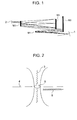
- Figure 1 shows an example of a 4:1 reduction X-ray exposure system able to meet the needs of the 0.10 ⁇ m generation.
- light from a light source is reflected at a mask 1 (or, while not shown, passing also possible), then is reflected at four mirrors (M1 to M4) and reaches a wafer 2.
- a pattern on a mask is transferred on a resist by exposure, then the wafer is conveyed out from the exposure system and the resist developed. Next, the resist selectively left on the wafer is used as a mask and for example a SiO2 layer or a metal interconnecting material etc. etched.
- a synchrotron radiation light can be considered a white light source having a sufficiently high brightness.
- the synchrotron radiation light can be shortened in wavelength to up to 100 keV (about 0.1 ⁇ ).
- synchrotron radiation light is basically a continuous wave (CW) light source.
- CW continuous wave
- Laser plasma light is generated by emission of a laser light for excitation on to a target.
- Laser plasma light can be increased in brightness by raising an output power of the excitation laser.
- the pulse width of the laser plasma light depends on the pulse width of the excitation laser, thus it is possible to shorten the pulse to a sub-picosecond order (about 100 fs).
- the wavelength generating high energy photons is determined by the characteristic X-rays of a target material. Therefore, the target must be changed for obtaining light of a different wavelength.
- a target material generating high energy photons of a wavelength not more than 1 ⁇ has not been obtained yet.
- the output power of an excitation laser and the pulse width of an excitation laser can be mentioned.
- Figure 2 is a schematic view of laser Compton scattering.
- the above-mentioned light source of short wavelength light comprises a reflecting means comprised of at least one pair of concave mirrors, a light emitting means for emitting light to the reflecting mean, and an electron beam generating means for emitting an electron beam 4 toward a light (preferably laser light) 3 emitted from the light emitting means and converged and repeatedly reflected at the reflecting mean. Due to the incidence of the electron beam 4, the light 3 and the electron beam 4 collide at a high density in a scattering region 5 and a scattered light (X-rays, for example) 6 can be obtained.
- Q-switched lasers enabling pulsed oscillation can be used.
- an Nd:YAG laser, a titanium-sapphire laser, and various kinds of excimer lasers such as a XeCl excimer laser, a KrF excimer laser, an ArF excimer laser, etc. or an X-ray laser can be mentioned.
- an apparatus able to generate an electron beam with an acceleration voltage of 100 keV or more and a velocity of about 0.5 X c (where c represents the velocity of light) or more such as an electron gun or an electron beam linear accelerator (Linac), can be used.
- the electron beam linear accelerator a traveling wave linear accelerator, a standing wave linear accelerator, an induction linear accelerator, a high voltage rectification accelerator (a Cockcroft-Walton accelerator, for example), a Van de Graff accelerator, a resonance transformer accelerator, etc. can be used.
- a traveling wave linear accelerator an Alvarez type, coupling cavity type, and high frequency quadrapole type, can be mentioned.
- the electron beam linear accelerator may be provided with a device for bunching electrons called a "buncher".
- the laser light is focused at the substantial center of the pair of concave mirrors and is reflected repeatedly between the concave mirrors. It is preferable that the pulse width of the laser beam be made to correspond to a beam diameter of the electron beam in order to make the electron beam and the laser beam collide precisely at the focus point.
- the acceleration energy of an electron beam can be mentioned. It is possible to control the wavelength of high energy photons by controlling the acceleration energy of the electron beam colliding with the laser beam.
- the angle of collision of the electron beam and the laser beam can be mentioned. It is possible to control the pulse width of the generated photon flux by controlling the collision angle.
- the output of the laser light is also a parameter. It becomes possible to raise the brightness of high energy photons by increasing the output of the laser light.
- the light source used for the semiconductor manufacturing apparatus of the present invention may be variable in wavelength or variable in pulse width.
- the yield ⁇ of scattered light in the inverse Compton scattering effect is represented as: ⁇ ⁇ N e N p s/A (N e : number of electrons, N p : number of photons, s: electron-photon scattering cross-section, A: cross-section of a region where two beams collide (scattering region)).
- the apparatus of the present embodiment stores an electron beam for a certain time in the scattering region where the electron beam and the laser beam collide.
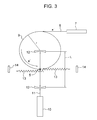
- Figure 3 is a schematic view of a light source part of the semiconductor manufacturing apparatus of the present invention. According to the apparatus shown in Fig. 3, it is possible to store electrons for a certain time and increase the yield ⁇ of scattered light.
- the electron beam 8 emitted from the electron beam source 7 is stored at an electron storage ring 9.
- laser light 11 emitted from a laser 10 is reflected at a mirror 12 and travels back and forth between the mirrors 12.
- the distance between the mirrors 12 becomes an resonator length L of laser Compton scattered light.
- the point of intersection of a circular orbit of electrons and the laser light 11 becomes a scattering region 5, where light having a shorter wavelength than the laser light 11 such as an X-ray 13 is emitted.
- a pair of X-ray mirrors 14 is arranged in the direction of emission of the X-ray 13, storage of high energy photons also becomes possible and it becomes possible to raise a brightness of high energy photons.
- N p ' 1 1- R ⁇ 10 4
- the light source of the semiconductor manufacturing apparatus of the present embodiment since 10 4 times the photons compared with the photons emitted from the laser is supplied to the resonator and are made to collide with the electrons in the electron storage ring, it is possible to greatly increase the yield ⁇ of the laser Compton scattered light.
- Examples 1 and 2 and Comparative Examples 1 and 2 show the results of ablation on a wafer with laser Compton scattered light using the above-mentioned inverse Compton scattering.
- Example 1 and Example 2 femtosecond pulses of 266 nm wavelength taken from a laser system shown in Fig. 4(A) were made to collide with the electron beam shown in Fig. 3 to generate laser Compton scattered light which is emitted on a wafer.
- nanosecond pulses of 266 nm wavelength taken from a laser system shown in Fig. 4(B) were made to collide with the electron beam shown in Fig. 3 to generate laser Compton scattered light which is emitted on a wafer.
- Example 1 the method of generating femtosecond pulses in Example 1 and Example 2 will be explained below.
- a pulsed oscillation mode-locked titanium-sapphire laser 22 was pumped with a CW oscillation argon ion laser 21.
- the laser light emitted from the titanium-sapphire laser 22 was 800 nm in wavelength and a pulse width of 100 fs, a pulse frequency of 80 MHZ, and an output of 1 W.
- the laser light from the titanium-sapphire laser 22 was guided to a pulse stretcher 23.
- the pulse width was stretched 2 to 4 orders at the pulse stretcher 23, then the light was guided to a titanium-sapphire amplifier 24.
- a three-stage amplifier comprised of a reproducing amplifier and multipass amplifiers was used.
- Pulsed light of the infrared region (800 nm in wavelength) from the pulse stretcher 23 was amplified by the titanium-sappire amplifier 24 and used for pumping a second harmonic of an Nd:YAG laser 25 (532 nm in wavelength, 1J in output, and 10 Hz in pulse frequency).
- the second harmonic from the Nd:YAG laser 25 pumped with the laser light from the titanium-sapphire laser 22 was guided to a pulse compressor 26 comprised of a diffraction grating etc. and again compressed to a pulse of femtoseconds.
- This femtosecond pulsed light (200 mJ) was guided to the fourth harmonic generator 27 to obtain a femtosecond pulse (266 nm in wavelength, pulse width of 200 fs, pulse energy of 60 mJ, beam diameter of 2 mm, and pulse frequency of 10 Hz).
- Teflon AF1600S (Du Pont, trademark) was coated on a silicon substrate by spin-coating to a thickness of about 1 ⁇ m to form a film.
- Example 1 400 pulses of the above-mentioned femtosecond pulsed laser Compton scattering light were emitted to the surface of the wafer made by the above-mentioned method through a mask having a line-and-space pattern of 0.3 ⁇ m. As a result, in the part exposed by the laser Compton scattered light, the Teflon layer was completely removed and the transfer of the pattern by ablation was recognized.
- a second harmonic from an Nd:YAG laser 25 (532 nm in wavelength, pulse width of 8 ns, output energy of 1 J, pulse frequency of 10 Hz) was guided to a fourth harmonic generator 27 to obtain a nanosecond pulse (266 nm in wavelength, pulse width of 8 ns, pulse energy of 180 mJ, and pulse frequency of 10 Hz).
- an ND (neutral density) filter was used to make the pulse energy 60 mJ.
- Comparative Example 1 400 pulses of the above mentioned nanosecond pulsed laser Compton scattered light were emitted to the surface of the wafer made by the same method as the above-mentioned Example 1 through a mask having a line-and-space pattern of 0.3 ⁇ m. As a result, the surface of the part exposed by the laser Compton scattered light was only roughed and the Teflon layer could not be removed.
- the ablation of the surface of the wafer was achieved by making the laser inducing the laser Compton scattered light ultra-short pulses with a pulse width of 1 ns or less.
- Example 2 wafers comprised of silicon substrates having oxide layers (SiO 2 layer) stacked on them were used as samples for evaluation of ablation.
- the surface of the wafers mentioned above were irradiated by 1000 pulses of the femtosecond pulsed laser Compton scattered light the same as the above mentioned Example 1 through a mask having a line-and-space pattern of 0.3 ⁇ m.
- the oxide layers were removed and clear transfer of the patterns by ablation was recognized.
- Comparative Example 2 the surface of a wafer the same as Example 2 mentioned above was irradiated by 1000 pulses of the nanosecond pulsed laser Compton scattered light the same as Comparative Example 1 mentioned above through a mask having a line-and-space pattern of 0.3 ⁇ m. As a result, there was an appreciable change in the part exposed by the laser Compton scattered light, but the oxide layer was not removed and the pattern was not transferred clearly.
- the ablation of the surface of the wafer was achieved by changing the laser inducing the laser Compton scattered light into ultra-short pulses with a pulse width of 1 ns or less.
- the semiconductor manufacturing apparatus of the above embodiment of the present invention it is made possible to emit light having a high brightness, high energy, and short pulse width on the surface of a wafer and to form a precise pattern by ablation.
- the semiconductor device manufacturing method of the above embodiment of the present invention it is possible to simplify the production process compared with the conventional patterning by etching, since the development of the resist and etching using a resist as a mask can be omitted.
- the embodiments of the semiconductor manufacturing apparatus and the semiconductor device manufacturing method of the present invention are not limited to the above explanation.
- the laser system for generating laser Compton scattered light may be suitably modified.
- the semiconductor manufacturing apparatus of the present invention it is made possible to form a fine pattern precisely on the surface of a wafer.
- the semiconductor device manufacturing method of the present invention it is made possible to form a pattern on the surface of a wafer with a simplified process compared with the case of etching using a resist as a mask.
- the semiconductor device manufacturing method of the present invention it is made possible to form a finer pattern clearly compared with the conventional ablation method.
Applications Claiming Priority (2)
| Application Number | Priority Date | Filing Date | Title |
|---|---|---|---|
| JP9497399 | 1999-04-01 | ||
| JP11094973A JP2000294523A (ja) | 1999-04-01 | 1999-04-01 | 半導体製造装置および半導体装置の製造方法 |
Publications (2)
| Publication Number | Publication Date |
|---|---|
| EP1041444A2 true EP1041444A2 (de) | 2000-10-04 |
| EP1041444A3 EP1041444A3 (de) | 2004-05-06 |
Family
ID=14124866
Family Applications (1)
| Application Number | Title | Priority Date | Filing Date |
|---|---|---|---|
| EP00400922A Withdrawn EP1041444A3 (de) | 1999-04-01 | 2000-04-03 | Vorrichtung und Verfahren zur Herstellung einer Halbleitervorrichtung |
Country Status (5)
| Country | Link |
|---|---|
| US (1) | US6549608B1 (de) |
| EP (1) | EP1041444A3 (de) |
| JP (1) | JP2000294523A (de) |
| KR (1) | KR20010006932A (de) |
| TW (1) | TW454428B (de) |
Families Citing this family (11)
| Publication number | Priority date | Publication date | Assignee | Title |
|---|---|---|---|---|
| JP4526732B2 (ja) * | 2001-05-17 | 2010-08-18 | 富士フイルム株式会社 | 光記録システム |
| JP2002333500A (ja) * | 2001-05-10 | 2002-11-22 | Sumitomo Heavy Ind Ltd | 短パルスx線発生装置及び発生方法 |
| US6760356B2 (en) * | 2002-04-08 | 2004-07-06 | The Regents Of The University Of California | Application of Yb:YAG short pulse laser system |
| US7351241B2 (en) * | 2003-06-02 | 2008-04-01 | Carl Zeiss Meditec Ag | Method and apparatus for precision working of material |
| KR101074389B1 (ko) * | 2004-11-05 | 2011-10-17 | 엘지디스플레이 주식회사 | 박막 식각 방법 및 이를 이용한 액정표시장치의 제조방법 |
| JP4925133B2 (ja) * | 2008-01-29 | 2012-04-25 | 独立行政法人産業技術総合研究所 | テラヘルツ波電子線分光測定方法および装置 |
| FR2935845B1 (fr) * | 2008-09-05 | 2010-09-10 | Centre Nat Rech Scient | Cavite optique amplificatrice de type fabry-perot |
| US8598016B2 (en) * | 2011-06-15 | 2013-12-03 | Applied Materials, Inc. | In-situ deposited mask layer for device singulation by laser scribing and plasma etch |
| US8557682B2 (en) * | 2011-06-15 | 2013-10-15 | Applied Materials, Inc. | Multi-layer mask for substrate dicing by laser and plasma etch |
| KR102163606B1 (ko) * | 2013-03-27 | 2020-10-08 | 고쿠리쓰다이가쿠호진 규슈다이가쿠 | 레이저 어닐링 장치 |
| US10342108B2 (en) | 2015-08-12 | 2019-07-02 | Asml Netherlands B.V. | Metrology methods, radiation source, metrology apparatus and device manufacturing method |
Citations (9)
| Publication number | Priority date | Publication date | Assignee | Title |
|---|---|---|---|---|
| US4414059A (en) * | 1982-12-09 | 1983-11-08 | International Business Machines Corporation | Far UV patterning of resist materials |
| EP0127861A2 (de) * | 1983-06-06 | 1984-12-12 | The University Of Rochester | Röntgenstrahl-Lithographie |
| GB2200219A (en) * | 1987-01-22 | 1988-07-27 | Rosser Roy J | Ultra-violet photo-ablative development of X-ray exposed photoresists |
| US4866517A (en) * | 1986-09-11 | 1989-09-12 | Hoya Corp. | Laser plasma X-ray generator capable of continuously generating X-rays |
| EP0357425A2 (de) * | 1988-09-02 | 1990-03-07 | Canon Kabushiki Kaisha | Belichtungseinrichtung |
| EP0531066A1 (de) * | 1991-09-03 | 1993-03-10 | Canon Kabushiki Kaisha | Synchrotron-Belichtungssystem und Verfahren zur Herstellung von Halbleitervorrichtungen unter Verwendung dieses Systems |
| WO1996033839A1 (en) * | 1995-04-26 | 1996-10-31 | Minnesota Mining And Manufacturing Company | Method and apparatus for step and repeat exposures |
| EP0858249A1 (de) * | 1997-02-07 | 1998-08-12 | Hitachi, Ltd. | Röntgenstrahlenquelle mittels laser erzeugtem Plasma, und Vorrichtung für Halbleiterlithographie und Verfahren unter Verwendung derselben |
| US5825847A (en) * | 1997-08-13 | 1998-10-20 | The Board Of Trustees Of The Leland Stanford Junior University | Compton backscattered collimated x-ray source |
Family Cites Families (2)
| Publication number | Priority date | Publication date | Assignee | Title |
|---|---|---|---|---|
| JPH0777160B2 (ja) * | 1989-07-26 | 1995-08-16 | 住友重機械工業株式会社 | 光蓄積リング |
| US5268951A (en) * | 1992-12-22 | 1993-12-07 | International Business Machines Corporation | X-ray beam scanning method for producing low distortion or constant distortion in x-ray proximity printing |
-
1999
- 1999-04-01 JP JP11094973A patent/JP2000294523A/ja active Pending
-
2000
- 2000-03-27 TW TW089105570A patent/TW454428B/zh not_active IP Right Cessation
- 2000-03-30 KR KR1020000016529A patent/KR20010006932A/ko active IP Right Grant
- 2000-03-30 US US09/538,737 patent/US6549608B1/en not_active Expired - Fee Related
- 2000-04-03 EP EP00400922A patent/EP1041444A3/de not_active Withdrawn
Patent Citations (9)
| Publication number | Priority date | Publication date | Assignee | Title |
|---|---|---|---|---|
| US4414059A (en) * | 1982-12-09 | 1983-11-08 | International Business Machines Corporation | Far UV patterning of resist materials |
| EP0127861A2 (de) * | 1983-06-06 | 1984-12-12 | The University Of Rochester | Röntgenstrahl-Lithographie |
| US4866517A (en) * | 1986-09-11 | 1989-09-12 | Hoya Corp. | Laser plasma X-ray generator capable of continuously generating X-rays |
| GB2200219A (en) * | 1987-01-22 | 1988-07-27 | Rosser Roy J | Ultra-violet photo-ablative development of X-ray exposed photoresists |
| EP0357425A2 (de) * | 1988-09-02 | 1990-03-07 | Canon Kabushiki Kaisha | Belichtungseinrichtung |
| EP0531066A1 (de) * | 1991-09-03 | 1993-03-10 | Canon Kabushiki Kaisha | Synchrotron-Belichtungssystem und Verfahren zur Herstellung von Halbleitervorrichtungen unter Verwendung dieses Systems |
| WO1996033839A1 (en) * | 1995-04-26 | 1996-10-31 | Minnesota Mining And Manufacturing Company | Method and apparatus for step and repeat exposures |
| EP0858249A1 (de) * | 1997-02-07 | 1998-08-12 | Hitachi, Ltd. | Röntgenstrahlenquelle mittels laser erzeugtem Plasma, und Vorrichtung für Halbleiterlithographie und Verfahren unter Verwendung derselben |
| US5825847A (en) * | 1997-08-13 | 1998-10-20 | The Board Of Trustees Of The Leland Stanford Junior University | Compton backscattered collimated x-ray source |
Non-Patent Citations (3)
| Title |
|---|
| KUEPER S ET AL: "ABLATION OF POLYTETRAFLUOROETHYLENE (TEFLON) WITH FEMTOSECOND UV EXCIMER LASER PULSES" APPLIED PHYSICS LETTERS, AMERICAN INSTITUTE OF PHYSICS. NEW YORK, US, vol. 54, no. 1, 1989, pages 4-6, XP000885253 ISSN: 0003-6951 * |
| SCHLACHTER A S ET AL: "THE ADVANCED LIGHT SOURCE AT LAWRENCE BERKELEY LABORATORY: A NEW TOOL FOR RESEARCH IN ATOMIC PHYSICS" NUCLEAR INSTRUMENTS & METHODS IN PHYSICS RESEARCH, SECTION - B: BEAM INTERACTIONS WITH MATERIALS AND ATOMS, NORTH-HOLLAND PUBLISHING COMPANY. AMSTERDAM, NL, vol. B53, no. 4, 3 April 1991 (1991-04-03), pages 512-517, XP000230312 ISSN: 0168-583X * |
| SRINIVASAN R ET AL: "INFLUENCE OF PULSE WIDTH ON ULTRAVIOLET LASER ABLATION OF POLY(METHYL METHACRYLATE)" APPLIED PHYSICS LETTERS, AMERICAN INSTITUTE OF PHYSICS. NEW YORK, US, vol. 53, no. 14, 1988, pages 1233-1235, XP000885254 ISSN: 0003-6951 * |
Also Published As
| Publication number | Publication date |
|---|---|
| KR20010006932A (ko) | 2001-01-26 |
| US6549608B1 (en) | 2003-04-15 |
| JP2000294523A (ja) | 2000-10-20 |
| TW454428B (en) | 2001-09-11 |
| EP1041444A3 (de) | 2004-05-06 |
Similar Documents
| Publication | Publication Date | Title |
|---|---|---|
| Elliott | Ultraviolet laser technology and applications | |
| JP5926521B2 (ja) | チャンバ装置 | |
| US6339634B1 (en) | Soft x-ray light source device | |
| EP0066053B1 (de) | Vorrichtung und Verfahren zur Belichtung eines lichtempfindlichen Mediums | |
| US6549608B1 (en) | Semiconductor manufacturing apparatus and semiconductor device manufacturing method | |
| US11737200B2 (en) | Residual gain monitoring and reduction for EUV drive laser | |
| KR20130038802A (ko) | 극단 자외 광 생성 장치 | |
| JP2021517662A (ja) | 光ビームの空間変調 | |
| Silfvast | Intense EUV incoherent plasma sources for EUV lithography and other applications | |
| JP4963149B2 (ja) | 光源装置及びそれを用いた露光装置 | |
| US20110122387A1 (en) | System and method for light source employing laser-produced plasma | |
| TWI591918B (zh) | 用於功率放大器之腔內損耗元件 | |
| CN113661446A (zh) | Euv辐射源和相关方法 | |
| US6903354B2 (en) | Extreme ultraviolet transition oscillator | |
| Newnam | Development of free-electron lasers for XUV projection lithography | |
| US10785859B2 (en) | Generating extreme ultraviolet radiation with nanoscale antennas | |
| JP2003001470A (ja) | レーザ加工装置およびレーザ加工方法 | |
| CN110612482B (zh) | 激光产生的等离子体源 | |
| JPH04167419A (ja) | レーザ露光装置 | |
| JP2000091195A (ja) | 露光方法及び露光装置 | |
| Endo et al. | Optimization of high average power FEL beam for EUV lithography application | |
| US6650678B1 (en) | Laser oscillating apparatus | |
| JPS6229785B2 (de) | ||
| JPWO2019069397A1 (ja) | レーザ加工方法及びレーザ加工システム | |
| JP5474891B2 (ja) | 光源装置及びそれを用いた露光装置 |
Legal Events
| Date | Code | Title | Description |
|---|---|---|---|
| PUAI | Public reference made under article 153(3) epc to a published international application that has entered the european phase |
Free format text: ORIGINAL CODE: 0009012 |
|
| AK | Designated contracting states |
Kind code of ref document: A2 Designated state(s): AT BE CH CY DE DK ES FI FR GB GR IE IT LI LU MC NL PT SE |
|
| AX | Request for extension of the european patent |
Free format text: AL;LT;LV;MK;RO;SI |
|
| PUAL | Search report despatched |
Free format text: ORIGINAL CODE: 0009013 |
|
| AK | Designated contracting states |
Kind code of ref document: A3 Designated state(s): AT BE CH CY DE DK ES FI FR GB GR IE IT LI LU MC NL PT SE |
|
| AX | Request for extension of the european patent |
Extension state: AL LT LV MK RO SI |
|
| 17P | Request for examination filed |
Effective date: 20041104 |
|
| AKX | Designation fees paid |
Designated state(s): DE FR |
|
| 17Q | First examination report despatched |
Effective date: 20050217 |
|
| STAA | Information on the status of an ep patent application or granted ep patent |
Free format text: STATUS: THE APPLICATION IS DEEMED TO BE WITHDRAWN |
|
| 18D | Application deemed to be withdrawn |
Effective date: 20061031 |