EP1039552B1 - Thin-film photoelectric conversion device and sputtering-deposition method - Google Patents
Thin-film photoelectric conversion device and sputtering-deposition method Download PDFInfo
- Publication number
- EP1039552B1 EP1039552B1 EP00301345A EP00301345A EP1039552B1 EP 1039552 B1 EP1039552 B1 EP 1039552B1 EP 00301345 A EP00301345 A EP 00301345A EP 00301345 A EP00301345 A EP 00301345A EP 1039552 B1 EP1039552 B1 EP 1039552B1
- Authority
- EP
- European Patent Office
- Prior art keywords
- layer
- substrate
- film
- holder
- photoelectric conversion
- Prior art date
- Legal status (The legal status is an assumption and is not a legal conclusion. Google has not performed a legal analysis and makes no representation as to the accuracy of the status listed.)
- Expired - Lifetime
Links
- 238000000151 deposition Methods 0.000 title claims abstract description 30
- 238000006243 chemical reaction Methods 0.000 title description 55
- 239000010409 thin film Substances 0.000 title description 47
- 239000000758 substrate Substances 0.000 claims abstract description 105
- 239000012212 insulator Substances 0.000 claims abstract description 38
- 230000002093 peripheral effect Effects 0.000 claims abstract description 34
- 125000006850 spacer group Chemical group 0.000 claims abstract description 19
- 238000004544 sputter deposition Methods 0.000 claims abstract description 15
- 238000000034 method Methods 0.000 claims description 13
- 229910052782 aluminium Inorganic materials 0.000 claims description 9
- XAGFODPZIPBFFR-UHFFFAOYSA-N aluminium Chemical compound [Al] XAGFODPZIPBFFR-UHFFFAOYSA-N 0.000 claims description 8
- 239000011888 foil Substances 0.000 claims description 5
- -1 polytetrafluoroethylene Polymers 0.000 claims description 4
- 239000004020 conductor Substances 0.000 claims description 3
- 229920001343 polytetrafluoroethylene Polymers 0.000 claims description 2
- 239000004810 polytetrafluoroethylene Substances 0.000 claims description 2
- 239000010408 film Substances 0.000 description 76
- 239000004065 semiconductor Substances 0.000 description 43
- BQCADISMDOOEFD-UHFFFAOYSA-N Silver Chemical compound [Ag] BQCADISMDOOEFD-UHFFFAOYSA-N 0.000 description 42
- 229910052709 silver Inorganic materials 0.000 description 40
- 239000004332 silver Substances 0.000 description 40
- 229910052751 metal Inorganic materials 0.000 description 21
- 239000002184 metal Substances 0.000 description 21
- 229920005989 resin Polymers 0.000 description 21
- 239000011347 resin Substances 0.000 description 21
- XLOMVQKBTHCTTD-UHFFFAOYSA-N Zinc monoxide Chemical compound [Zn]=O XLOMVQKBTHCTTD-UHFFFAOYSA-N 0.000 description 20
- RTAQQCXQSZGOHL-UHFFFAOYSA-N Titanium Chemical compound [Ti] RTAQQCXQSZGOHL-UHFFFAOYSA-N 0.000 description 18
- 239000010936 titanium Substances 0.000 description 18
- 229910052719 titanium Inorganic materials 0.000 description 18
- 239000011521 glass Substances 0.000 description 17
- 230000000052 comparative effect Effects 0.000 description 16
- 238000007789 sealing Methods 0.000 description 14
- 238000002955 isolation Methods 0.000 description 12
- 239000012298 atmosphere Substances 0.000 description 11
- 230000008021 deposition Effects 0.000 description 11
- 239000011787 zinc oxide Substances 0.000 description 10
- 239000000853 adhesive Substances 0.000 description 9
- 230000001070 adhesive effect Effects 0.000 description 8
- 238000007599 discharging Methods 0.000 description 7
- 238000004519 manufacturing process Methods 0.000 description 7
- 229910052946 acanthite Inorganic materials 0.000 description 6
- XUARKZBEFFVFRG-UHFFFAOYSA-N silver sulfide Chemical compound [S-2].[Ag+].[Ag+] XUARKZBEFFVFRG-UHFFFAOYSA-N 0.000 description 6
- 229940056910 silver sulfide Drugs 0.000 description 6
- XOLBLPGZBRYERU-UHFFFAOYSA-N tin dioxide Chemical compound O=[Sn]=O XOLBLPGZBRYERU-UHFFFAOYSA-N 0.000 description 6
- 229910001887 tin oxide Inorganic materials 0.000 description 6
- VYPSYNLAJGMNEJ-UHFFFAOYSA-N Silicium dioxide Chemical compound O=[Si]=O VYPSYNLAJGMNEJ-UHFFFAOYSA-N 0.000 description 5
- 230000015572 biosynthetic process Effects 0.000 description 5
- 229910010271 silicon carbide Inorganic materials 0.000 description 5
- XLYOFNOQVPJJNP-UHFFFAOYSA-N water Substances O XLYOFNOQVPJJNP-UHFFFAOYSA-N 0.000 description 5
- XUIMIQQOPSSXEZ-UHFFFAOYSA-N Silicon Chemical compound [Si] XUIMIQQOPSSXEZ-UHFFFAOYSA-N 0.000 description 4
- 238000002441 X-ray diffraction Methods 0.000 description 4
- 229910021417 amorphous silicon Inorganic materials 0.000 description 4
- 230000015556 catabolic process Effects 0.000 description 4
- 238000005229 chemical vapour deposition Methods 0.000 description 4
- 238000006731 degradation reaction Methods 0.000 description 4
- 239000000463 material Substances 0.000 description 4
- 239000002245 particle Substances 0.000 description 4
- 238000005268 plasma chemical vapour deposition Methods 0.000 description 4
- 229910052710 silicon Inorganic materials 0.000 description 4
- 239000010703 silicon Substances 0.000 description 4
- 241000245026 Scoliopus bigelovii Species 0.000 description 3
- BLRPTPMANUNPDV-UHFFFAOYSA-N Silane Chemical compound [SiH4] BLRPTPMANUNPDV-UHFFFAOYSA-N 0.000 description 3
- NINIDFKCEFEMDL-UHFFFAOYSA-N Sulfur Chemical compound [S] NINIDFKCEFEMDL-UHFFFAOYSA-N 0.000 description 3
- 235000012467 brownies Nutrition 0.000 description 3
- 239000002019 doping agent Substances 0.000 description 3
- 238000001704 evaporation Methods 0.000 description 3
- 230000008020 evaporation Effects 0.000 description 3
- 238000002474 experimental method Methods 0.000 description 3
- 239000000945 filler Substances 0.000 description 3
- 229910010272 inorganic material Inorganic materials 0.000 description 3
- 239000011147 inorganic material Substances 0.000 description 3
- 150000002500 ions Chemical class 0.000 description 3
- 238000001755 magnetron sputter deposition Methods 0.000 description 3
- 229910021424 microcrystalline silicon Inorganic materials 0.000 description 3
- 238000000059 patterning Methods 0.000 description 3
- HBMJWWWQQXIZIP-UHFFFAOYSA-N silicon carbide Chemical class [Si+]#[C-] HBMJWWWQQXIZIP-UHFFFAOYSA-N 0.000 description 3
- 229910052717 sulfur Inorganic materials 0.000 description 3
- 239000011593 sulfur Substances 0.000 description 3
- 229910001316 Ag alloy Inorganic materials 0.000 description 2
- XKRFYHLGVUSROY-UHFFFAOYSA-N Argon Chemical compound [Ar] XKRFYHLGVUSROY-UHFFFAOYSA-N 0.000 description 2
- ZOXJGFHDIHLPTG-UHFFFAOYSA-N Boron Chemical compound [B] ZOXJGFHDIHLPTG-UHFFFAOYSA-N 0.000 description 2
- OKTJSMMVPCPJKN-UHFFFAOYSA-N Carbon Chemical compound [C] OKTJSMMVPCPJKN-UHFFFAOYSA-N 0.000 description 2
- RYGMFSIKBFXOCR-UHFFFAOYSA-N Copper Chemical compound [Cu] RYGMFSIKBFXOCR-UHFFFAOYSA-N 0.000 description 2
- UFHFLCQGNIYNRP-UHFFFAOYSA-N Hydrogen Chemical compound [H][H] UFHFLCQGNIYNRP-UHFFFAOYSA-N 0.000 description 2
- OAICVXFJPJFONN-UHFFFAOYSA-N Phosphorus Chemical compound [P] OAICVXFJPJFONN-UHFFFAOYSA-N 0.000 description 2
- 229920002367 Polyisobutene Polymers 0.000 description 2
- 229910000577 Silicon-germanium Inorganic materials 0.000 description 2
- 239000004809 Teflon Substances 0.000 description 2
- 229920006362 Teflon® Polymers 0.000 description 2
- LEVVHYCKPQWKOP-UHFFFAOYSA-N [Si].[Ge] Chemical compound [Si].[Ge] LEVVHYCKPQWKOP-UHFFFAOYSA-N 0.000 description 2
- 229910052796 boron Inorganic materials 0.000 description 2
- 229910052799 carbon Inorganic materials 0.000 description 2
- 229910052681 coesite Inorganic materials 0.000 description 2
- 239000003086 colorant Substances 0.000 description 2
- 239000011889 copper foil Substances 0.000 description 2
- 229910052906 cristobalite Inorganic materials 0.000 description 2
- 230000006378 damage Effects 0.000 description 2
- 230000000593 degrading effect Effects 0.000 description 2
- 230000002542 deteriorative effect Effects 0.000 description 2
- 229910052739 hydrogen Inorganic materials 0.000 description 2
- 239000001257 hydrogen Substances 0.000 description 2
- 238000009413 insulation Methods 0.000 description 2
- 150000004767 nitrides Chemical class 0.000 description 2
- 229910052698 phosphorus Inorganic materials 0.000 description 2
- 239000011574 phosphorus Substances 0.000 description 2
- BASFCYQUMIYNBI-UHFFFAOYSA-N platinum Chemical compound [Pt] BASFCYQUMIYNBI-UHFFFAOYSA-N 0.000 description 2
- 229920002037 poly(vinyl butyral) polymer Polymers 0.000 description 2
- 229920000139 polyethylene terephthalate Polymers 0.000 description 2
- 239000005020 polyethylene terephthalate Substances 0.000 description 2
- 238000010248 power generation Methods 0.000 description 2
- 239000000377 silicon dioxide Substances 0.000 description 2
- 229910000679 solder Inorganic materials 0.000 description 2
- 239000010935 stainless steel Substances 0.000 description 2
- 229910001220 stainless steel Inorganic materials 0.000 description 2
- 229910052682 stishovite Inorganic materials 0.000 description 2
- 229910052905 tridymite Inorganic materials 0.000 description 2
- 238000001947 vapour-phase growth Methods 0.000 description 2
- 238000004833 X-ray photoelectron spectroscopy Methods 0.000 description 1
- 229910052786 argon Inorganic materials 0.000 description 1
- 238000003491 array Methods 0.000 description 1
- 229910052785 arsenic Inorganic materials 0.000 description 1
- RQNWIZPPADIBDY-UHFFFAOYSA-N arsenic atom Chemical compound [As] RQNWIZPPADIBDY-UHFFFAOYSA-N 0.000 description 1
- 239000010953 base metal Substances 0.000 description 1
- 229910052804 chromium Inorganic materials 0.000 description 1
- 229920006026 co-polymeric resin Polymers 0.000 description 1
- 229910021419 crystalline silicon Inorganic materials 0.000 description 1
- 230000000694 effects Effects 0.000 description 1
- 238000005401 electroluminescence Methods 0.000 description 1
- 239000005038 ethylene vinyl acetate Substances 0.000 description 1
- 239000007789 gas Substances 0.000 description 1
- PCHJSUWPFVWCPO-UHFFFAOYSA-N gold Chemical compound [Au] PCHJSUWPFVWCPO-UHFFFAOYSA-N 0.000 description 1
- 229910052737 gold Inorganic materials 0.000 description 1
- 239000010931 gold Substances 0.000 description 1
- AMGQUBHHOARCQH-UHFFFAOYSA-N indium;oxotin Chemical compound [In].[Sn]=O AMGQUBHHOARCQH-UHFFFAOYSA-N 0.000 description 1
- 238000013383 initial experiment Methods 0.000 description 1
- 238000009434 installation Methods 0.000 description 1
- 238000003475 lamination Methods 0.000 description 1
- 239000007769 metal material Substances 0.000 description 1
- 229910000510 noble metal Inorganic materials 0.000 description 1
- TWNQGVIAIRXVLR-UHFFFAOYSA-N oxo(oxoalumanyloxy)alumane Chemical compound O=[Al]O[Al]=O TWNQGVIAIRXVLR-UHFFFAOYSA-N 0.000 description 1
- 238000000016 photochemical curing Methods 0.000 description 1
- 229910052697 platinum Inorganic materials 0.000 description 1
- 229920001200 poly(ethylene-vinyl acetate) Polymers 0.000 description 1
- 229920002620 polyvinyl fluoride Polymers 0.000 description 1
- 238000000926 separation method Methods 0.000 description 1
- 230000009528 severe injury Effects 0.000 description 1
- 150000003376 silicon Chemical class 0.000 description 1
- 229910052814 silicon oxide Inorganic materials 0.000 description 1
- 239000005361 soda-lime glass Substances 0.000 description 1
- 238000002230 thermal chemical vapour deposition Methods 0.000 description 1
- 229920005992 thermoplastic resin Polymers 0.000 description 1
- 229920001187 thermosetting polymer Polymers 0.000 description 1
- 230000000007 visual effect Effects 0.000 description 1
- 238000003466 welding Methods 0.000 description 1
Images


Classifications
-
- H—ELECTRICITY
- H10—SEMICONDUCTOR DEVICES; ELECTRIC SOLID-STATE DEVICES NOT OTHERWISE PROVIDED FOR
- H10F—INORGANIC SEMICONDUCTOR DEVICES SENSITIVE TO INFRARED RADIATION, LIGHT, ELECTROMAGNETIC RADIATION OF SHORTER WAVELENGTH OR CORPUSCULAR RADIATION
- H10F71/00—Manufacture or treatment of devices covered by this subclass
-
- H—ELECTRICITY
- H10—SEMICONDUCTOR DEVICES; ELECTRIC SOLID-STATE DEVICES NOT OTHERWISE PROVIDED FOR
- H10F—INORGANIC SEMICONDUCTOR DEVICES SENSITIVE TO INFRARED RADIATION, LIGHT, ELECTROMAGNETIC RADIATION OF SHORTER WAVELENGTH OR CORPUSCULAR RADIATION
- H10F19/00—Integrated devices, or assemblies of multiple devices, comprising at least one photovoltaic cell covered by group H10F10/00, e.g. photovoltaic modules
- H10F19/30—Integrated devices, or assemblies of multiple devices, comprising at least one photovoltaic cell covered by group H10F10/00, e.g. photovoltaic modules comprising thin-film photovoltaic cells
- H10F19/31—Integrated devices, or assemblies of multiple devices, comprising at least one photovoltaic cell covered by group H10F10/00, e.g. photovoltaic modules comprising thin-film photovoltaic cells having multiple laterally adjacent thin-film photovoltaic cells deposited on the same substrate
- H10F19/33—Patterning processes to connect the photovoltaic cells, e.g. laser cutting of conductive or active layers
-
- H—ELECTRICITY
- H10—SEMICONDUCTOR DEVICES; ELECTRIC SOLID-STATE DEVICES NOT OTHERWISE PROVIDED FOR
- H10F—INORGANIC SEMICONDUCTOR DEVICES SENSITIVE TO INFRARED RADIATION, LIGHT, ELECTROMAGNETIC RADIATION OF SHORTER WAVELENGTH OR CORPUSCULAR RADIATION
- H10F19/00—Integrated devices, or assemblies of multiple devices, comprising at least one photovoltaic cell covered by group H10F10/00, e.g. photovoltaic modules
- H10F19/80—Encapsulations or containers for integrated devices, or assemblies of multiple devices, having photovoltaic cells
- H10F19/85—Protective back sheets
-
- H—ELECTRICITY
- H10—SEMICONDUCTOR DEVICES; ELECTRIC SOLID-STATE DEVICES NOT OTHERWISE PROVIDED FOR
- H10F—INORGANIC SEMICONDUCTOR DEVICES SENSITIVE TO INFRARED RADIATION, LIGHT, ELECTROMAGNETIC RADIATION OF SHORTER WAVELENGTH OR CORPUSCULAR RADIATION
- H10F77/00—Constructional details of devices covered by this subclass
- H10F77/40—Optical elements or arrangements
- H10F77/42—Optical elements or arrangements directly associated or integrated with photovoltaic cells, e.g. light-reflecting means or light-concentrating means
- H10F77/48—Back surface reflectors [BSR]
-
- Y—GENERAL TAGGING OF NEW TECHNOLOGICAL DEVELOPMENTS; GENERAL TAGGING OF CROSS-SECTIONAL TECHNOLOGIES SPANNING OVER SEVERAL SECTIONS OF THE IPC; TECHNICAL SUBJECTS COVERED BY FORMER USPC CROSS-REFERENCE ART COLLECTIONS [XRACs] AND DIGESTS
- Y02—TECHNOLOGIES OR APPLICATIONS FOR MITIGATION OR ADAPTATION AGAINST CLIMATE CHANGE
- Y02E—REDUCTION OF GREENHOUSE GAS [GHG] EMISSIONS, RELATED TO ENERGY GENERATION, TRANSMISSION OR DISTRIBUTION
- Y02E10/00—Energy generation through renewable energy sources
- Y02E10/50—Photovoltaic [PV] energy
- Y02E10/52—PV systems with concentrators
Definitions
- the present invention relates to sputtering-deposition methods usable in manufacturing thin-film photoelectric conversion devices, and in particular to a sputtering-deposition method used in forming a back metal electrode layer of a thin-film photoelectric conversion device that is formed on a transparent insulator substrate.
- Thin-film solar batteries, TFT (Thin-Film Transistor) arrays, mirrors and the like require that a film including at least one conductive layer be formed on an insulator substrate.
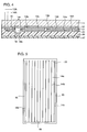
- Fig. 1 is a schematic cross section showing an exemplary conventional sputtering-deposition method used to form on an insulator substrate a film including at least one conductive layer.
- a substrate holder 1 is initially prepared.
- Substrate holder 1 is generally in the form of a frame with an opening 1a at its central area.
- Substrate holder 1 preferably has along a peripheral edge of opening 1a a step 1b for accepting substrate 2.
- substrate holder 1 is formed of a conductive material such as stainless steel and electrically grounded.
- an insulator substrate 2 such as a glass plate is positioned to be fit on step 1b to cover opening 1a.
- a back plate 3 formed of a conductive plate, such as an aluminum plate or a carbon plate. Back plate 3 is fixed to holder 1 with a screw or bolt 4 to press insulator substrate 2 against conductive holder 1.
- metal, oxide, nitride or the like is sputtered to deposit a layer thereof on a region of insulator substrate 2 exposed in the holder's opening 1a.
- Ar ions used in general to sputter a target and sputtered particles to contribute to the film deposition are positively charged.
- a conductive layer of metal, transparent conductive oxide (TCO) or the like is formed on insulator substrate 2
- an additional conductive layer of metal, TCO or the like is formed on a surface of a layered structure including at least one conductive layer already formed on insulator substrate 2, as in a case of forming a back electrode to fabricate a thin-film solar battery with a transparent electrode, a semiconductor layer and the back electrode successively formed on a transparent insulator substrate of glass or the like, or when a layer of a metal such as Cr (a conductive layer) is initially formed on transparent insulator substrate 2 such as a glass plate and then an insulating layer is formed on the metal layer, as in a case of forming a gate insulating film of a TFT, the positive charge of Ar ions and sputtered particles flying toward and colliding against insulator substrate 2 is transferred to the conductive layer on the substrate.
- conductive substrate holder 1 is earthe
- a back electrode is formed through deposition at an almost final step of the whole process, i.e., after forming a transparent electrode layer on a glass substrate, patterning the transparent electrode layer, forming a semiconductor layer such as a thin film of amorphous silicon, crystalline silicon or the like, and patterning the semiconductor layer.
- a semiconductor layer such as a thin film of amorphous silicon, crystalline silicon or the like
- Solar battery modules are often installed on roofs and walls of buildings and in such case they play a role as parts of the buildings.
- a thin-film solar battery module with a continuous browny color across the entire surface of a transparent insulator substrate such as a glass plate is preferable to a monocrystalline-type solar battery module including a plurality of mutually discontinuous monocrystalline cells joined to a glass substrate.
- a thin-film solar battery module is fabricated by successively stacking a transparent electrode layer, a semiconductor layer and a metal electrode layer on a transparent insulator substrate through vapor-phase deposition.
- the region for forming the semiconductor layer and that for forming the metal electrode layer are set to be substantially identical.
- an actually deposited metal electrode layer has a peripheral edge region positionally offset and thus protruding from a peripheral edge of the semiconductor layer, then as seen from a light-incident side of the transparent substrate the peripheral edge region of the metal electrode layer can be disadvantageously observed in the form of a white line showing outside the dark browny peripheral edge of the semiconductor layer region to spoil a unified good appearance of the thin-film solar battery module.
- a sealing resin material of white color or similar colors is normally used to protect back surfaces of a plurality of monocrystalline cells of the module and if such material is applied to protect a back surface of a thin-film solar battery module then the module has an appearance with its semiconductor layer region's peripheral edge surrounded by a white frame and thus has an aesthetically degraded appearance.
- a thin-film solar battery module in general a transparent electrode layer, a semiconductor layer and a metal electrode layer stacked on a substrate are for example laser-scribed and thus divided into a plurality of photoelectric conversion cells which are in turn electrically interconnected and thus integrated.
- An industrial standard of thin-film solar battery modules requires that a cell region be insulated from any peripheral edge region outside the cell region, and accordingly a thin-film solar battery module typically has a cell region laser-scribed and thus electrically isolated from any peripheral edge region that may electrically contact a frame holding the module.
- the semiconductor region deposited on the transparent insulator substrate is inward of a peripheral edge of the metal electrode layer deposited on the semiconductor region and at a location for forming the aforementioned peripheral isolation groove the metal electrode layer directly contact the transparent electrode layer or the transparent insulator substrate, then a laser beam incident on and transmitted through the transparent substrate to laser-scribe the metal electrode layer can hardly form a satisfactory groove in the metal layer due to its high reflectance and thus often fails to provide a sufficient withstand voltage.
- a thin-film solar battery module typically has a back electrode covered with an organic protection film with a sealing resin layer therebetween to prevent its back metal layer from deteriorating while the module is used outdoor and also to prevent its power generation performance from temporarily lowering when rain droplets, dews and the like adhere between the photoelectric conversion cells of the module.
- a thin-film solar battery module has a back electrode layer formed of a highly reflective metal material to more efficiently use incident light in its semiconductor layer for photoelectric conversion. More specifically, light which is not absorbed in the semiconductor layer and is thus transmitted therethrough can be reflected by the highly reflective back metal layer back into the semiconductor layer and the reflected light can also be absorbed in the semiconductor layer and thus photoelectrically converted to provide an improved photoelectric conversion efficiency of the thin-film solar battery module.
- the back electrode layer is often formed of silver or a silver alloy in view of light reflectance and conductivity. Silver, however, readily deteriorates when it is exposed to the atmosphere, since it reacts with a sulfur-containing gaseous component such as SOx contained in the atmosphere and on its surface a silver sulfide is produced.
- Such degrading reaction proceeds with time and can reach inside the back electrode layer.
- a thin-film solar battery module is used outdoor over a long time period, its back electrode layer, even protected with organic film, deteriorates as described above. This can result in a degraded adherence between the back electrode layer and the organic film and hence peeling of the protection film and a reduced conductivity of the back electrode layer.
- a back electrode layer can react with a sulfur component in the atmosphere and thus be degraded significantly not only while a thin-film solar battery module including the back electrode layer is used outdoor but while the module is fabricated. More specifically, if even for a short time period between formation of the back electrode layer and application of a sealing resin and an organic protection film the silver-containing back electrode layer is directly exposed to the atmosphere, then the layer's surface immediately reacts with the sulfur component in the atmosphere. Needless to say, the reaction degrading the back electrode layer can proceed deeper inside the back electrode layer if the layer is longer exposed to the atmosphere.
- JP 05263237 discloses a method of producing a transparent electrode film in which secondary electrodes are captured by an anode between an ITO target and a substrate.
- US 4 494 699 discloses a method of producing an electroluminescence device in which a first installation layer is deposited by sputtering.
- the object of the present invention is to provide a sputtering-deposition method capable of preventing a conductive layer from being charged up and thus discharging when a film including at least one such conductive layer is formed on an insulator substrate.
- the method of the present invention can provide a solar battery module having a peripheral edge region with an improved appearance, and improved stability and reliability of a photoelectric conversion device having a silver-containing back electrode layer.
- a sputtering-deposition method according to claim 1 is provided.
- the spacer may be previously arranged on and fixed to the back plate.
- the spacer can be formed of polytetrafluoroethylene (e.g. Teflon ® ) or an aluminum foil.
- the present inventors have found from the following facts that with the conventional sputtering-deposition method as shown in Fig. 1 it is difficult to completely prevent a conductive layer on insulator substrate 2 from being charged up and thus discharging.
- the present inventors prepared glass substrate 2 having a TCO layer on the entirety of its lower surface and set substrate 2 on conductive holder 1, as shown in Fig. 1 . Then, a tester was used to measure the electrical conduction between the TCO layer and holder 1 in the vicinity of a perimeter of the substrate's opening 1a and a resistance no more than 1 ⁇ was obtained.
- Fig. 2 is a schematic cross section showing a sputtering-deposition method according to the present invention.
- substrate holder 1 is initially prepared as in the Fig. 1 conventional example.
- Substrate holder 1 is generally in the form of a frame with opening 1a at its central area.
- substrate holder 1 preferably has along a peripheral edge of opening 1a a step 1b for accepting substrate 2.
- substrate holder 1 is formed of a conductive material such as stainless steel, and it is electrically earthed.
- insulator substrate 2 such as a glass plate is positioned to fit on step 1b to cover opening 1a.
- spacer 5 formed of a flexible material such as Teflon ® or an aluminum foil is arranged on a peripheral edge of insulator substrate 2.
- Spacer 5 can be sized, shaped and arranged, as appropriately selected.
- back plate 3 formed of a conductive plate such as an aluminum plate or a carbon plate is superposed on insulator substrate 2 with spacer 5 therebetween to cover the entirety of the back surface of insulator substrate 2.
- Back plate 3 is fixed to holder 1 with a screw or a bolt 4 such that back plate 3 presses insulator substrate 2 against conductive holder 1.
- the means to fix back plate 3 to holder 1 is not limited to the screw or the bolt and it may be other means, such as a clip or a clamp.
- metal, oxide, nitride or the like can be sputtered and a layer thereof can be deposited on a region of insulator substrate 2 which is exposed in the conductive holder's opening 1a.
- a conductive layer such as a metal layer or a TCO layer
- the conductive layer on insulator substrate 2 can be prevented from being charged up and thus discharging, to provide for a significantly improved film-production yield.
- flexible spacer 5 between substrate 2 and back plate 3 can prevent substrate 2 from being damaged while it enables a planar contact rather than a point contact to be maintained between conductive layer 1 and substrate 2 and as a result the electric charge transferred from charged particles to the conductive layer on insulator substrate 2 can be released to the earth via conductive holder 1.
- glass substrate 2 with a TCO layer formed on the entirety of its lower surface was mounted on conductive holder 1 and an Ag layer was deposited on substrate 2 through sputtering. As a result it was found that the conductive layer on glass substrate 2 was not charged up and did not discharge.
- any discharge attributable to charge-up did not occur either when a glass substrate with a transparent electrode and a semiconductor layer successively stacked thereon was mounted on conductive holder 1 and then an Ag layer was deposited thereon through sputtering.
- the following is considered other than the phenomena previously described. More specifically, owing to the planar contact between the conductive holder and the substrate, there may be continuity of the deposited conductive film between the conductive holder and the substrate and hence an electrical conduction therebetween. It may be evidence thereof that a conductive layer formed directly on an insulator substrate held on this holder was much less frequently charged up and discharged.
- Fig. 3 is a schematic plan view of back plate 3 with such spacer 5 previously arranged thereon, positioned as appropriate, and fixed thereto. It should be noted, however, that spacer 5 is not limited in size, shape or arrangement as shown in Fig. 3 and it can be selected as appropriate depending on the properties, size and shape of the substrate. Spacer 5 can be fixed to back plate 3 by means of an adhesive agent, screwing, welding and the like.
- the present invention provides for a sputtering-deposition method capable of preventing a conductive layer from being charged up and thus discharging when a film including at least one such conductive layer is formed on an insulator substrate, realizing a significantly improved production yield.
- Fig. 4 is a schematic cross section of an integrated thin-film solar battery module formed using the method of the present invention.
- a tin oxide film as a transparent electrode layer 12 having a thickness of approximately 800 nm was formed by thermal CVD (chemical vapor deposition). It should be noted that the tin oxide film may be replaced with another film of TCO such as ITO (indium-tin oxide) or zinc oxide.
- Transparent electrode layer 12 was then laser-scribed to form a plurality of transparent-electrode isolation grooves 12b to divide transparent electrode layer 12 into a plurality of transparent electrode strips 12a extending in a direction orthogonal to the plane of Fig. 4 .
- glass substrate 11 was set on an X-Y table and a beam from a Q switch YAG laser was directed through substrate 11 and focused to irradiate transparent electrode layer 12.
- the second harmonic having a wavelength of 532 nm was used, with a pulse frequency of 3 kHz, an average output of 500 mW, and a pulse width of 10 nsec.
- Each transparent electrode 12a formed was approximately 10 nm wide and each groove 12b was approximately 50 ⁇ m wide.
- a substrate supporting frame was used to cover the substrate's peripheral edge portion by a width of 3 mm.
- Semiconductor layer 13 was formed of a p-type a-SiC:H (amorphous hydrogenated silicon carbide) sublayer, an i-type a-Si:H sublayer, and an n-type ⁇ c-Si:H (microcrystalline hydrogenated silicon) sublayer successively deposited to provide a p-i-n semiconductor junction.
- the p-, i- and n-type sublayers were each deposited in a separate chamber of an in-line type plasma CVD apparatus.
- SiH 4 at 100 sccm (standard cubic centimeter per minute), hydrogen at 200 sccm containing B 2 H 6 of 1000 ppm, and CH 4 at 30 sccm were used with a pressure of 133 Pa (1Torr) and a high-frequency source power of 200W applied.
- the p-type sublayer was deposited to have a thickness of approximately 15 nm.
- SiH 4 at 500 sccm was used with a pressure of 67 Pa (0.5 Torr) and a source power of 500W applied.
- the i-type layer was deposited to have a thickness of approximately 320 nm.
- n-type sublayer SiH 4 at 100 sccm and hydrogen at 200 sccm containing PH 3 of 1000 ppm were used with a pressure of 133 Pa and a source power of 3 kW applied.
- the n-type layer was deposited to have a thickness of approximately 30 nm.
- semiconductor layer 13 was laser-scribed to form a plurality of semiconductor-layer division grooves 13b to divide the layer into a plurality of semiconductor regions 13a.
- the laser-scribing conditions in this case were the same as those in patterning transparent electrode layer 12, except that depth of focus the laser beam was changed.
- Each semiconductor-layer division groove 13b was 100 ⁇ m wide and spaced by 100 ⁇ m from transparent-electrode isolation groove 12b adjacent thereto.
- a zinc oxide film of 100 nm thickness and a silver film of 200 nm thickness were stacked as a back electrode layer 14 on patterned semiconductor layer 13a in a region 14A 4mm inward of any perimeters of substrate 11.
- the zinc oxide film acts to maintain the silver film's high reflectance and also to prevent silver atoms from diffusing into semiconductor layer 13.
- another film of a metal may be used such as Al, Cr, Ti or the like.
- the zinc oxide film was deposited through magnetron sputtering.
- As the sputtering conditions an argon gas pressure of 0.27 Pa (2 mTorr), a high-frequency source power of 200W and a deposition temperature of 200°C were used.
- the silver film was also deposited through magnetron sputtering.
- the sputtering conditions used for the silver film was different from those used for the zinc oxide film only in that a direct-current power supply was used for the deposition at a room temperature.
- Back electrode layer 14 was laser-scribed to form a plurality of back-electrode isolation grooves 14b and thus it was divided into a plurality of back electrodes 14a.
- the laser-scribing conditions in this case were exactly the same as those for formation of semiconductor-layer division groove 13b, and together with a local region of semiconductor layer 13 having absorbed the laser beam, back electrode layer 14 thereon was locally brown away to form back-electrode isolation groove 14b each having a width of 70 ⁇ m and spaced by 100 ⁇ m from semiconductor-layer division groove 13b adjacent thereto.
- bus bar electrode connection groove 14c was laser-scribed. While bus bar electrode connection region 14c in Fig. 4 is shown with semiconductor layer 13 and back electrode layer 14 both completely removed, it may be provided in a form of a bunch of multiple grooves, since a copper foil 18 as a bus bar electrode can be connected later by solder 18a to transparent electrode 12a through the bunch of groove.
- peripheral isolation groove 15 was formed 5 mm inward of the perimeter of substrate 11.
- Peripheral isolation groove 15 was formed to have a width of 150 ⁇ m and also penetrated transparent electrode layer 12, semiconductor layer 13 and back electrode layer 14.
- peripheral isolation groove 15 along the perimeter of substrate 11 is shown in a schematic plan view. While Fig. 5 shows a limited number of back electrodes 14a to simplify the drawing, in practice 50 back electrodes were included.
- Copper foil electrode 18 was then joined by solder 18a to each of bus bar electrode connection regions 14c provided at opposite ends of the plurality of photoelectric conversion cells interconnected in series. Then, the photoelectric conversion cells were integrated and had their back surfaces protected by an EVA (ethylene-vinyleacetate copolymer) resin filler 8 and a fluororesin film 9. While typically an EVA resin is transparent and a fluororesin film is also transparent or has white color, the present invention employs those colored dark. More specifically, the present invention adopts dark colors such as black, brown or wine red.
- EVA ethylene-vinyleacetate copolymer
- the obtained, integrated thin-film solar battery module was illuminated by a solar simulator with a light of AM1.5 having an energy density of 100 mW/cm 2 , and it exhibited photoelectric conversion characteristics of a short-circuit current of 1240 mA, an open-circuit voltage of 44.2V, a fill factor of 0.68, and a maximum output of 37.3W.
- a solar simulator with a light of AM1.5 having an energy density of 100 mW/cm 2 , and it exhibited photoelectric conversion characteristics of a short-circuit current of 1240 mA, an open-circuit voltage of 44.2V, a fill factor of 0.68, and a maximum output of 37.3W.
- five integrated thin-film solar batteries were fabricated and they all presented generally similar photoelectric conversion characteristics.
- FIG. 6 As a comparative example related to the Fig. 4 example, an integrated thin-film solar battery was fabricated as shown in Fig. 6 .
- the Fig. 6 solar battery is distinguished from the Fig. 4 solar battery only in that semiconductor layer 13 and back electrode layer 14 were deposited with a substrate supporting frame covering a peripheral edge of substrate 11 by a width of 5 mm.
- Five such comparative solar batteries were fabricated. Because of an unavoidable slight positional offset between semiconductor layer deposition region 13A and back electrode layer deposition region 14A, back electrode layer 14 had a peripheral region protruding from at least one side of a rectangular outer perimeter of semiconductor layer deposition region 13A and thus observed as a thin while line.
- three of the five solar batteries of the Fig. 6 comparative example presented photoelectric conversion characteristics substantially equivalent to those of the Fig. 4 example, the remaining two solar batteries had faulty insulation with respect to peripheral isolation groove 15.
- the integrated thin-film solar battery module can have an appearance with its surface uniformly having a dark browny color. Furthermore, insulation and separation between the cell formation region and the peripheral edge can be ensured without an additional fabrication step, to provide an increased production yield of such integrated thin-film solar battery modules.
- Fig. 7 is a schematic cross section of a semiconductor thin-film photoelectric conversion cell formed using the method of the present invention.
- Fig. 7 shows only a single photoelectric conversion cell to simplify the drawing. It is needless to say, however, that this photoelectric conversion cell can also be applied to the integrated thin-film solar battery module as shown in Fig. 4 .
- the semiconductor thin-film photoelectric conversion cell may have a transparent substrate 21 formed of a glass plate, a transparent resin film or the like.
- a transparent electrode 22 of tin oxide, ITO, zinc oxide or the like.
- Transparent electrode 21 may have a monolayered structure or a multilayered structure formed of TCO of different kinds and can be formed through a known vapor phase deposition, such as evaporation, chemical vapor deposition, sputtering or the like.
- transparent electrode layer 22 has a surface having a textured surface structure with fine unevenness.
- a textured surface structure of transparent electrode layer 22 can act to scatter and introduce light into a semiconductor thin-film photoelectric conversion unit 23 fabricated thereon, to contribute to providing an improved photoelectric conversion efficiency.
- semiconductor thin-film photoelectric conversion unit 23 formed on transparent electrode layer 22 includes a p-type semiconductor layer 23p, an i-type semiconductor photoelectric conversion layer 23i and an n-type semiconductor layer 23n, all of which semiconductor layers can be deposited by plasma CVD.
- P-type semiconductor layer 23p can be formed of silicon or silicon carbide and is doped with atoms of a p-type conductivity-type determining dopant such as boron or aluminum.
- Photoelectric conversion layer 23i on p-type semiconductor layer 23p can be formed of substantially intrinsic semiconductor, such as silicon, silicon carbide, silicon germanium or the like.
- Photoelectric conversion layer 23i may also be formed of a weak p- or n-type semiconductor material containing a slight amount of conductivity-type determining dopant atoms, as long as the resulting layer has a sufficient photoelectric conversion capability.
- Photoelectric conversion layer 23i is typically formed to have a thickness in a range of 0.1 to 10 ⁇ m.
- N-type semiconductor layer 23n on photoelectric conversion layer 23i can be formed of silicon or silicon germanium and is doped with atoms of an n-type conductivity-type determining dopant, such as phosphorus or arsenic.
- Back electrode layer 24 can be formed of silver or a silver alloy, though it is typically formed of silver in view of high reflectance and conductivity.
- a thin TCO layer such as zinc oxide.
- Such TCO layer can act to prevent back electrode layer 24 from having a degraded light reflectance and also to prevent silver atoms from diffusing into photoelectric conversion unit 23.
- Back electrode 24 can be formed through evaporation, sputtering or the like.
- Back electrode layer 24 has not its upper surface 24a but side surface 24b covered with an inorganic protection film 25. More specifically, inorganic protection film 25 is formed to have a structure capping back electrode 24.
- Inorganic protection layer 25 is formed of an inorganic material stable against air and water, e.g., a noble metal such as gold or platinum, a base metal forming a passive-state film in the atmosphere such as aluminum or titanium, or an oxide such as silicon oxide, aluminum oxide or zinc oxide, and it may have a monolayered structure or a multilayered structure.
- a noble metal such as gold or platinum
- a base metal forming a passive-state film in the atmosphere
- Such inorganic materials can also have a superior adhesiveness with sealing resin 26 provided thereon.
- titanium can be particularly preferably used as inorganic protection film 25 because of its ability to prevent degradation of silver-containing back electrode layer 24 and its adherence to sealing resin 26.
- Inorganic protection layer 25 can be deposited through evaporation, sputtering, chemical vapor deposition or the like. Inorganic protection film 25 has a thickness set in a range of 0.5 to 100 nm, preferably 2 to 10 nm.
- inorganic protection film 25 covers and thus isolates upper and side surfaces 24a and 24b of silver-containing back electrode layer 24 from the external environment. While back electrode layer 24 may cover the upper surface of photoelectric conversion unit 23 entirely, preferably back electrode layer 24 has a peripheral edge slightly inward of a peripheral edge of photoelectric conversion unit 23, as shown in Fig. 7 . In other words, photoelectric conversion unit 23 preferably has an upper surface with a peripheral edge region slightly protruding from the peripheral edge of back electrode layer 24. As such, inorganic protection film 25 can not only cover upper and side surfaces 24a and 24b of back electrode 24 but be joined to the upper peripheral edge region of photoelectric conversion unit 23 to more reliably seal and hence protect back electrode 24. It should be noted that such upper peripheral exposed region of photoelectric conversion unit 23 is only desired to have a width W equivalent to the thickness of inorganic protection layer 25.
- the photoelectric conversion cell with silver-containing back electrode layer 24 having both upper and side surfaces 24a and 24b covered with inorganic protection film 25 of titanium or the like, ensures that back electrode layer 24 is prevented from deteriorating in subsequent fabrication steps.
- inorganic protection film 25 of titanium or the like
- Sealing resin layer 26 applied onto inorganic protection film 25 can be a type of resin capable of sealing the photoelectric conversion cells and adhering to organic protection film 27.
- Such sealing resin 26 may be thermoplastic resin, thermosetting resin or photocuring resin, and more specifically it can be EVA (ethylenevinylacetate copolymer), PVB (polyvinyl butyral), PIB (polyisobutylene), silicon resin or the like.
- Organic protection film 27 may include at least one insulator film highly resistant to moisture and water, e.g., a fluororesin film such as polyvinyl fluoride (e.g., Tedler ® film), or PET (poly ethylene terephthalate film.
- Organic protection film 27 may also have a laminated structure sandwiching a metal foil formed, e.g., of aluminum, since such a foil acts to enhance moisture resistance, water resistance and the like and thus more effectively protects the photoelectric conversion cells from moisture.
- sealing resin 26 and organic protection film 27 as described above can be joined simultaneously to the back surfaces of the photoelectric conversion cells through vacuum lamination. Since inorganic protection film 25 itself is stable against air and water, its initial adherence to sealing resin 26 is sufficient. As such if an integrated thin-film solar battery module including a plurality of the Fig. 7 photoelectric conversion cells is used outdoor for a long time period, the photoelectric conversion cells can be reliably protected by sealing resin 26 and organic protection film 27.
- degradation of silver-containing back electrode 24 can be detected by x-ray analysis (x-ray photoelectron spectroscopy) of silver sulfide and that the adherence of sealing resin 26 and organic protection film 27 to inorganic protection film 25 can be known by measuring the force required for peeling organic protection film 27 from an end of the back surface of the photoelectric conversion device.
- x-ray analysis x-ray photoelectron spectroscopy
- An integrated thin-film solar battery module including a plurality of the Fig. 7 photoelectric conversion cells was fabricated as described below. Initially, a glass substrate 21 was prepared, having a major surface on which a SiO 2 layer (not shown) of 50 nm thickness was formed. Deposited on the SiO 2 layer was a tin oxide film 22 having an uneven surface texture, F-doped, and having a thickness of approximately 800 nm. Tin oxide film 22 was laser-scribed and thus patterned in a plurality of transparent electrodes.
- plasma CVD was carried out to successively deposit on tin oxide film 22 a p-type a-SiC: H layer 23n of 15 nm thickness, an i-type a-Si: H layer 23i of 400 nm thickness, and an n-type ⁇ c-Si: H layer 23n of 30 nm thickness.
- P-type n-SiC: H layer 23n was doped with boron
- i-type a-Si: H layer 23i is non-doped
- n-type ⁇ c-Si:H layer 23n was doped with phosphorus.
- photoelectric conversion unit 23 was obtained including a p-i-n junction.
- an in-line type magnetron sputtering apparatus was used to successively deposit a zinc oxide layer (not shown) of 80 nm in thickness and a silver electrode layer 24 of 200 nm thickness.
- the zinc oxide layer and silver electrode layer 24 were deposited using a mask having an opening slightly smaller than the region of each photoelectric conversion unit 23.
- each silver electrode 24 by using a mask having a slightly larger opening than the mask used for deposition of each silver electrode 24, sputtering was carried out to form a titanium layer 25 having a thickness of 5 nm to cover the silver electrode's upper and side surfaces 24a and 24b.
- the mask used for deposition of each silver electrode 24 can also be used to deposit titanium layer 25. More specifically, by placing the mask slightly farther from substrate 21 in depositing titanium film 25 than in depositing silver electrode 24, titanium atoms can travel around a peripheral edge of the mask's opening to cover the silver electrode's side surface 24b.
- An integrated thin-film solar battery was thus fabricated with a plurality of photoelectric conversion cells interconnected in series as shown in Fig. 4 and the battery was left in the atmosphere for no less than 200 hours. Then, silver electrode layer 24 was subjected to x-ray analysis and any silver sulfide was not detected nor did the layer's surface have any change in color observed.
- Tedler ® film 27 was stuck onto titanium layer 25 with EVA filler resin 26 therebetween to obtain the photoelectric conversion device as shown in Fig. 7 .
- An integrated thin-film solar battery module similar to the above specific example was fabricated except that titanium that protection film 25 was not provided. More specifically, after silver electrode layer 24 was formed, the layer was left for one hour in the atmosphere and then covered with EVA resin filler 26 and Tedler ® film 27.
- An integrated thin-film solar battery module of comparative example 2 was fabricated similar to that of comparative example 1, except that it is left in the atmosphere for 12 hours after formation of silver electrode layer 24.
- silver electrode layer 24 was found through visual observation to have a surface changed in color, yellowish. Furthermore, silver electrode layer 24 was subjected to x-ray analysis, and silver electrode layer 24 exposed to air for a shorter time period had silver sulfide detected only at its surface and silver electrode layer 24 exposed to air for a longer time period had silver sulfide also detected at its deeper portion.
- An integrated thin-film solar battery module of comparative example 3 was fabricated similar to the above specific example, except that the silver electrode's upper surface 24a was covered with protection film 25 of titanium whereas its side surface 24b was not. After titanium protection film 25 was provided only on the silver electrode layer's upper surface 24a, the module was exposed to air for 200 hours and silver electrode layer 24 was then subjected to x-ray analysis. Silver electrode 24 had a small amount of silver sulfide detected at a peripheral edge thereof.
- the integrated thin-film solar battery modules of the specific example and comparative examples 1-3 thus fabricated were measured for the adhesive strength between EVA layer 26 and Tedler ® film 27. More specifically, measured as the adhesive strength therebetween was a force required per unit width for partially peeling EVA layer 26 and Tedler ® film 27 from silver electrode layer 24 or titanium protection layer 25 and continuing such peeling.
- the measured adhesive strength at a center of silver electrode 24 was approximately 5 kgf/cm in comparative example 1, but was reduced to approximately 0.7 kgf/cm in comparative example 2.
- a conventional thin-film photoelectric conversion device with a silver electrode layer exposed to air for a simply increased time period from 1 hour to 12 hours has a significantly reduced adhesive strength of sealing resin layer 26 and Tedler ® film 27.
- EVA layer 26 and Tedler ® film 27 had an adhesive strength of no less than approximately 5 kgf/cm at a center of titanium protection film 25 and they also had at a peripheral edge of titanium protection film 25 an adhesive strength equivalent to that obtained at the center of titanium protection film 25.
- the thin-film photoelectric conversion device of the specific example can maintain a sufficiently high adhesive strength of EVA layer 26 and Tedler ® film 27 with respect to titanium protection layer 25 over an extremely long time period, and thus prevent degradation of silver electrode layer 24.
- the present invention can provide a highly reliable thin-film photoelectric conversion device with a silver-containing back electrode layer having not only its upper surface but also side surface covered with an inorganic protection film stable against air and water to prevent degradation of the silver-containing back electrode layer.
Landscapes
- Photovoltaic Devices (AREA)
- Physical Vapour Deposition (AREA)
- Light Receiving Elements (AREA)
- Physical Deposition Of Substances That Are Components Of Semiconductor Devices (AREA)
Abstract
Description
- The present invention relates to sputtering-deposition methods usable in manufacturing thin-film photoelectric conversion devices, and in particular to a sputtering-deposition method used in forming a back metal electrode layer of a thin-film photoelectric conversion device that is formed on a transparent insulator substrate.
- Thin-film solar batteries, TFT (Thin-Film Transistor) arrays, mirrors and the like require that a film including at least one conductive layer be formed on an insulator substrate.
-
Fig. 1 is a schematic cross section showing an exemplary conventional sputtering-deposition method used to form on an insulator substrate a film including at least one conductive layer. In this sputtering-deposition method, asubstrate holder 1 is initially prepared.Substrate holder 1 is generally in the form of a frame with an opening 1a at its central area.Substrate holder 1 preferably has along a peripheral edge of opening 1a astep 1b for acceptingsubstrate 2. Furthermore,substrate holder 1 is formed of a conductive material such as stainless steel and electrically grounded. - On
conductive substrate holder 1, aninsulator substrate 2 such as a glass plate is positioned to be fit onstep 1b to coveropening 1a. Superposed oninsulator substrate 2 is aback plate 3 formed of a conductive plate, such as an aluminum plate or a carbon plate.Back plate 3 is fixed to holder 1 with a screw orbolt 4 to pressinsulator substrate 2 againstconductive holder 1. - In such condition, metal, oxide, nitride or the like is sputtered to deposit a layer thereof on a region of
insulator substrate 2 exposed in the holder'sopening 1a. In such film deposition through sputtering, Ar ions used in general to sputter a target and sputtered particles to contribute to the film deposition are positively charged. As such, when a conductive layer of metal, transparent conductive oxide (TCO) or the like is formed oninsulator substrate 2, when an additional conductive layer of metal, TCO or the like is formed on a surface of a layered structure including at least one conductive layer already formed oninsulator substrate 2, as in a case of forming a back electrode to fabricate a thin-film solar battery with a transparent electrode, a semiconductor layer and the back electrode successively formed on a transparent insulator substrate of glass or the like, or when a layer of a metal such as Cr (a conductive layer) is initially formed ontransparent insulator substrate 2 such as a glass plate and then an insulating layer is formed on the metal layer, as in a case of forming a gate insulating film of a TFT, the positive charge of Ar ions and sputtered particles flying toward and colliding againstinsulator substrate 2 is transferred to the conductive layer on the substrate. To release the electric charge transferred to the conductive layer oninsulator substrate 2,conductive substrate holder 1 is earthed. - If
substrate 2 is electrically floating fromconductive holder 1, however, the electric charge from Ar ions and sputtered particles is accumulated in the conductive layer oninsulator substrate 2 and voltage of the conductive layer is increased, and when the voltage of the conductive layer exceeds a certain value, the layer discharges as if a thunder were caused. The discharge occurs between the conductive layer onsubstrate 2 and the target or other portions of the sputtering apparatus, and such portions suffer damage traces due to the discharge. As a result, the film onsubstrate 2 is severely damaged and the whole substrate must be discarded. - In particular, for an integrated thin-film solar battery, a back electrode is formed through deposition at an almost final step of the whole process, i.e., after forming a transparent electrode layer on a glass substrate, patterning the transparent electrode layer, forming a semiconductor layer such as a thin film of amorphous silicon, crystalline silicon or the like, and patterning the semiconductor layer. As such, the discharge damage of the back electrode leads to economically severe damage and it is a matter of concern.
- With the recent heightened public awareness of protection of global environment, solar power generation is increasingly used as a clean energy source. Solar battery modules are often installed on roofs and walls of buildings and in such case they play a role as parts of the buildings. As such, architects demand a solar battery module having an appearance harmonious with the building of interest, in particular that having a color tone harmonious with the building. As such, for example a thin-film solar battery module with a continuous browny color across the entire surface of a transparent insulator substrate such as a glass plate, is preferable to a monocrystalline-type solar battery module including a plurality of mutually discontinuous monocrystalline cells joined to a glass substrate.
- In general, a thin-film solar battery module is fabricated by successively stacking a transparent electrode layer, a semiconductor layer and a metal electrode layer on a transparent insulator substrate through vapor-phase deposition. In stacking the layers, normally the region for forming the semiconductor layer and that for forming the metal electrode layer are set to be substantially identical. As such, if an actually deposited metal electrode layer has a peripheral edge region positionally offset and thus protruding from a peripheral edge of the semiconductor layer, then as seen from a light-incident side of the transparent substrate the peripheral edge region of the metal electrode layer can be disadvantageously observed in the form of a white line showing outside the dark browny peripheral edge of the semiconductor layer region to spoil a unified good appearance of the thin-film solar battery module.
- Furthermore for a monocrystalline-type solar battery module a sealing resin material of white color or similar colors is normally used to protect back surfaces of a plurality of monocrystalline cells of the module and if such material is applied to protect a back surface of a thin-film solar battery module then the module has an appearance with its semiconductor layer region's peripheral edge surrounded by a white frame and thus has an aesthetically degraded appearance.
- In a thin-film solar battery module, in general a transparent electrode layer, a semiconductor layer and a metal electrode layer stacked on a substrate are for example laser-scribed and thus divided into a plurality of photoelectric conversion cells which are in turn electrically interconnected and thus integrated. An industrial standard of thin-film solar battery modules requires that a cell region be insulated from any peripheral edge region outside the cell region, and accordingly a thin-film solar battery module typically has a cell region laser-scribed and thus electrically isolated from any peripheral edge region that may electrically contact a frame holding the module. As such, if the semiconductor region deposited on the transparent insulator substrate is inward of a peripheral edge of the metal electrode layer deposited on the semiconductor region and at a location for forming the aforementioned peripheral isolation groove the metal electrode layer directly contact the transparent electrode layer or the transparent insulator substrate, then a laser beam incident on and transmitted through the transparent substrate to laser-scribe the metal electrode layer can hardly form a satisfactory groove in the metal layer due to its high reflectance and thus often fails to provide a sufficient withstand voltage.
- A thin-film solar battery module typically has a back electrode covered with an organic protection film with a sealing resin layer therebetween to prevent its back metal layer from deteriorating while the module is used outdoor and also to prevent its power generation performance from temporarily lowering when rain droplets, dews and the like adhere between the photoelectric conversion cells of the module.
- A thin-film solar battery module has a back electrode layer formed of a highly reflective metal material to more efficiently use incident light in its semiconductor layer for photoelectric conversion. More specifically, light which is not absorbed in the semiconductor layer and is thus transmitted therethrough can be reflected by the highly reflective back metal layer back into the semiconductor layer and the reflected light can also be absorbed in the semiconductor layer and thus photoelectrically converted to provide an improved photoelectric conversion efficiency of the thin-film solar battery module. The back electrode layer is often formed of silver or a silver alloy in view of light reflectance and conductivity. Silver, however, readily deteriorates when it is exposed to the atmosphere, since it reacts with a sulfur-containing gaseous component such as SOx contained in the atmosphere and on its surface a silver sulfide is produced. Such degrading reaction proceeds with time and can reach inside the back electrode layer. As such, if a thin-film solar battery module is used outdoor over a long time period, its back electrode layer, even protected with organic film, deteriorates as described above. This can result in a degraded adherence between the back electrode layer and the organic film and hence peeling of the protection film and a reduced conductivity of the back electrode layer.
- According to a recent study by the present inventors, it has been found that a back electrode layer can react with a sulfur component in the atmosphere and thus be degraded significantly not only while a thin-film solar battery module including the back electrode layer is used outdoor but while the module is fabricated. More specifically, if even for a short time period between formation of the back electrode layer and application of a sealing resin and an organic protection film the silver-containing back electrode layer is directly exposed to the atmosphere, then the layer's surface immediately reacts with the sulfur component in the atmosphere. Needless to say, the reaction degrading the back electrode layer can proceed deeper inside the back electrode layer if the layer is longer exposed to the atmosphere.
-
JP 05263237 -
US 4 494 699 discloses a method of producing an electroluminescence device in which a first installation layer is deposited by sputtering. - In view of the aforementioned related art, the object of the present invention is to provide a sputtering-deposition method capable of preventing a conductive layer from being charged up and thus discharging when a film including at least one such conductive layer is formed on an insulator substrate.
- The method of the present invention can provide a solar battery module having a peripheral edge region with an improved appearance, and improved stability and reliability of a photoelectric conversion device having a silver-containing back electrode layer.
- In the present invention, a sputtering-deposition method according to
claim 1 is provided. - It should be noted that the spacer may be previously arranged on and fixed to the back plate. Furthermore, the spacer can be formed of polytetrafluoroethylene (e.g. Teflon®) or an aluminum foil.
- The foregoing and other objects, features, aspects and advantages of the present invention will become more apparent from the following detailed description of the present invention when taken in conjunction with the accompanying drawings.
-
-
Fig. 1 is a schematic cross section showing a substrate holding structure in a conventional sputtering-deposition method. -
Fig. 2 is a schematic cross section showing a substrate holding structure in a sputtering-deposition method according to the present invention. -
Fig. 3 is a schematic plan view showing an exemplary back plate that can be preferably used in the sputtering-deposition method shown inFig. 2 . -
Fig. 4 is a schematic cross section of a thin-film solar battery module formed using the method of the present invention. -
Fig. 5 is a schematic plan view showing a peripheral isolation groove in theFig. 4 thin-film solar battery module. -
Fig. 6 is a cross section of a thin-film solar battery module as a comparative example with respect to theFig. 4 embodiment. -
Fig. 7 is a schematic cross section showing a thin-film photoelectric conversion device formed using the method of the present invention. - First of all, the present inventors have found from the following facts that with the conventional sputtering-deposition method as shown in
Fig. 1 it is difficult to completely prevent a conductive layer oninsulator substrate 2 from being charged up and thus discharging. - As an initial experiment, assuming deposition of a back electrode for a thin-film solar battery, a glass substrate with a transparent electrode and a semiconductor layer stacked thereon was prepared and set on
conductive holder 1 as shown inFig. 1 and then subjected to sputtering to deposit a film thereon. In this experiment there were observed occasional discharging phenomena attributed to charging-up, though it was difficult to grasp the discharging phenomena in detail and it seemed that another experiment should be conducted using a simpler system. Accordingly, withonly glass substrate 2 set similarly on theFig. 1 conductive holder 1, a conductive layer was experimentally deposited and there were still such discharging phenomena occasionally observed. In this experiment there was no means to quantitatively measure electrical conduction of contact between the substrate and the holder and it was thus believed that such means was necessary. - Accordingly, the present inventors prepared
glass substrate 2 having a TCO layer on the entirety of its lower surface and setsubstrate 2 onconductive holder 1, as shown inFig. 1 . Then, a tester was used to measure the electrical conduction between the TCO layer andholder 1 in the vicinity of a perimeter of the substrate'sopening 1a and a resistance no more than 1 Ω was obtained. - However, discharge occurred when an Ag layer was deposited on the TCO layer through sputtering. On the other hand,
glass substrate 2 was damaged whenscrew 4 was screwed too tightly to ensure contact betweensubstrate 2 andconductive holder 1. -
Fig. 2 is a schematic cross section showing a sputtering-deposition method according to the present invention. In this sputtering-deposition method also,substrate holder 1 is initially prepared as in theFig. 1 conventional example.Substrate holder 1 is generally in the form of a frame withopening 1a at its central area. Furthermore,substrate holder 1 preferably has along a peripheral edge of opening 1a astep 1b for acceptingsubstrate 2. Furthermore,substrate holder 1 is formed of a conductive material such as stainless steel, and it is electrically earthed. - On such
conductive substrate holder 1,insulator substrate 2 such as a glass plate is positioned to fit onstep 1b to coveropening 1a. - In contrast with the conventional example, a
spacer 5 formed of a flexible material such as Teflon® or an aluminum foil is arranged on a peripheral edge ofinsulator substrate 2.Spacer 5 can be sized, shaped and arranged, as appropriately selected. - Then, back
plate 3 formed of a conductive plate such as an aluminum plate or a carbon plate is superposed oninsulator substrate 2 withspacer 5 therebetween to cover the entirety of the back surface ofinsulator substrate 2. Backplate 3 is fixed toholder 1 with a screw or abolt 4 such thatback plate 3 pressesinsulator substrate 2 againstconductive holder 1. It is needless to say, however, that the means to fix backplate 3 toholder 1 is not limited to the screw or the bolt and it may be other means, such as a clip or a clamp. - In the condition as shown in
Fig. 2 , metal, oxide, nitride or the like can be sputtered and a layer thereof can be deposited on a region ofinsulator substrate 2 which is exposed in the conductive holder'sopening 1a. As such, when a conductive layer such as a metal layer or a TCO layer is formed oninsulator substrate 2 or when at least one conductive layer is initially formed oninsulator substrate 2 and an insulator layer is then deposited on the conductive layer, the conductive layer oninsulator substrate 2 can be prevented from being charged up and thus discharging, to provide for a significantly improved film-production yield. This may be becauseflexible spacer 5 betweensubstrate 2 andback plate 3 can preventsubstrate 2 from being damaged while it enables a planar contact rather than a point contact to be maintained betweenconductive layer 1 andsubstrate 2 and as a result the electric charge transferred from charged particles to the conductive layer oninsulator substrate 2 can be released to the earth viaconductive holder 1. - In accordance with the
Fig. 2 method,glass substrate 2 with a TCO layer formed on the entirety of its lower surface was mounted onconductive holder 1 and an Ag layer was deposited onsubstrate 2 through sputtering. As a result it was found that the conductive layer onglass substrate 2 was not charged up and did not discharge. - Furthermore, it has been found that any discharge attributable to charge-up did not occur either when a glass substrate with a transparent electrode and a semiconductor layer successively stacked thereon was mounted on
conductive holder 1 and then an Ag layer was deposited thereon through sputtering. As a principle of this effect, the following is considered other than the phenomena previously described. More specifically, owing to the planar contact between the conductive holder and the substrate, there may be continuity of the deposited conductive film between the conductive holder and the substrate and hence an electrical conduction therebetween. It may be evidence thereof that a conductive layer formed directly on an insulator substrate held on this holder was much less frequently charged up and discharged. - For the sputtering-deposition method as shown In
Fig. 2 , afterinsulator substrate 2 is positioned on the conductive holder'sstep 1b, separate flexible spacers may be arranged along the substrate's peripheral edge portion and backplate 3 may then be superposed thereon. To simplify the process, however, it is preferable thatspacer 5 be previously fixed onback plate 3.Fig. 3 is a schematic plan view ofback plate 3 withsuch spacer 5 previously arranged thereon, positioned as appropriate, and fixed thereto. It should be noted, however, thatspacer 5 is not limited in size, shape or arrangement as shown inFig. 3 and it can be selected as appropriate depending on the properties, size and shape of the substrate.Spacer 5 can be fixed to backplate 3 by means of an adhesive agent, screwing, welding and the like. - Thus the present invention provides for a sputtering-deposition method capable of preventing a conductive layer from being charged up and thus discharging when a film including at least one such conductive layer is formed on an insulator substrate, realizing a significantly improved production yield.
-
Fig. 4 is a schematic cross section of an integrated thin-film solar battery module formed using the method of the present invention. To fabricate this solar battery, initially on a soda-lime-glass substrate 11 having an area of 92 cm × 46 cm and a thickness of 4 mm, a tin oxide film as atransparent electrode layer 12 having a thickness of approximately 800 nm was formed by thermal CVD (chemical vapor deposition). It should be noted that the tin oxide film may be replaced with another film of TCO such as ITO (indium-tin oxide) or zinc oxide. -
Transparent electrode layer 12 was then laser-scribed to form a plurality of transparent-electrode isolation grooves 12b to dividetransparent electrode layer 12 into a plurality oftransparent electrode strips 12a extending in a direction orthogonal to the plane ofFig. 4 . To laser-pattern the layer,glass substrate 11 was set on an X-Y table and a beam from a Q switch YAG laser was directed throughsubstrate 11 and focused to irradiatetransparent electrode layer 12. As a laser condition, the second harmonic having a wavelength of 532 nm was used, with a pulse frequency of 3 kHz, an average output of 500 mW, and a pulse width of 10 nsec. Eachtransparent electrode 12a formed was approximately 10 nm wide and eachgroove 12b was approximately 50 µm wide. - Then, plasma CVD was employed to deposit a
semiconductor layer 13 on patternedtransparent electrode layer 12 in aregion 13A three millimeters inward of any perimeters ofsubstrate 11. In this CVD, a substrate supporting frame was used to cover the substrate's peripheral edge portion by a width of 3 mm.Semiconductor layer 13 was formed of a p-type a-SiC:H (amorphous hydrogenated silicon carbide) sublayer, an i-type a-Si:H sublayer, and an n-type µc-Si:H (microcrystalline hydrogenated silicon) sublayer successively deposited to provide a p-i-n semiconductor junction. The p-, i- and n-type sublayers were each deposited in a separate chamber of an in-line type plasma CVD apparatus. - To deposit the p-type sublayer, SiH4 at 100 sccm (standard cubic centimeter per minute), hydrogen at 200 sccm containing B2H6 of 1000 ppm, and CH4 at 30 sccm were used with a pressure of 133 Pa (1Torr) and a high-frequency source power of 200W applied. The p-type sublayer was deposited to have a thickness of approximately 15 nm. To deposit the i-type sublayer, SiH4 at 500 sccm was used with a pressure of 67 Pa (0.5 Torr) and a source power of 500W applied. The i-type layer was deposited to have a thickness of approximately 320 nm. To deposit the n-type sublayer, SiH4 at 100 sccm and hydrogen at 200 sccm containing PH3 of 1000 ppm were used with a pressure of 133 Pa and a source power of 3 kW applied. The n-type layer was deposited to have a thickness of approximately 30 nm.
- Then,
semiconductor layer 13 was laser-scribed to form a plurality of semiconductor-layer division grooves 13b to divide the layer into a plurality ofsemiconductor regions 13a. The laser-scribing conditions in this case were the same as those in patterningtransparent electrode layer 12, except that depth of focus the laser beam was changed. Each semiconductor-layer division groove 13b was 100 µm wide and spaced by 100 µm from transparent-electrode isolation groove 12b adjacent thereto. - Then, a zinc oxide film of 100 nm thickness and a silver film of 200 nm thickness were stacked as a
back electrode layer 14 on patternedsemiconductor layer 13a in aregion 14A 4mm inward of any perimeters ofsubstrate 11. The zinc oxide film acts to maintain the silver film's high reflectance and also to prevent silver atoms from diffusing intosemiconductor layer 13. As an alternative to the silver film, another film of a metal may be used such as Al, Cr, Ti or the like. - The zinc oxide film was deposited through magnetron sputtering. As the sputtering conditions, an argon gas pressure of 0.27 Pa (2 mTorr), a high-frequency source power of 200W and a deposition temperature of 200°C were used. The silver film was also deposited through magnetron sputtering. The sputtering conditions used for the silver film was different from those used for the zinc oxide film only in that a direct-current power supply was used for the deposition at a room temperature.
-
Back electrode layer 14 was laser-scribed to form a plurality of back-electrode isolation grooves 14b and thus it was divided into a plurality ofback electrodes 14a. The laser-scribing conditions in this case were exactly the same as those for formation of semiconductor-layer division groove 13b, and together with a local region ofsemiconductor layer 13 having absorbed the laser beam,back electrode layer 14 thereon was locally brown away to form back-electrode isolation groove 14b each having a width of 70 µm and spaced by 100 µm from semiconductor-layer division groove 13b adjacent thereto. - After back
electrode isolation groove 14b was formed, a bus barelectrode connection groove 14c was laser-scribed. While bus barelectrode connection region 14c inFig. 4 is shown withsemiconductor layer 13 and backelectrode layer 14 both completely removed, it may be provided in a form of a bunch of multiple grooves, since acopper foil 18 as a bus bar electrode can be connected later bysolder 18a totransparent electrode 12a through the bunch of groove. - Then, by laser-scribing similarly in forming transparent-
electrode isolation groove 12b, aperipheral isolation groove 15 was formed 5 mm inward of the perimeter ofsubstrate 11.Peripheral isolation groove 15 was formed to have a width of 150 µm and also penetratedtransparent electrode layer 12,semiconductor layer 13 and backelectrode layer 14. InFig. 5 ,peripheral isolation groove 15 along the perimeter ofsubstrate 11 is shown in a schematic plan view. WhileFig. 5 shows a limited number ofback electrodes 14a to simplify the drawing, in practice 50 back electrodes were included. -
Copper foil electrode 18 was then joined bysolder 18a to each of bus barelectrode connection regions 14c provided at opposite ends of the plurality of photoelectric conversion cells interconnected in series. Then, the photoelectric conversion cells were integrated and had their back surfaces protected by an EVA (ethylene-vinyleacetate copolymer) resin filler 8 and a fluororesin film 9. While typically an EVA resin is transparent and a fluororesin film is also transparent or has white color, the present invention employs those colored dark. More specifically, the present invention adopts dark colors such as black, brown or wine red. - The obtained, integrated thin-film solar battery module was illuminated by a solar simulator with a light of AM1.5 having an energy density of 100 mW/cm2, and it exhibited photoelectric conversion characteristics of a short-circuit current of 1240 mA, an open-circuit voltage of 44.2V, a fill factor of 0.68, and a maximum output of 37.3W. In the present example, five integrated thin-film solar batteries were fabricated and they all presented generally similar photoelectric conversion characteristics.
- As a comparative example related to the
Fig. 4 example, an integrated thin-film solar battery was fabricated as shown inFig. 6 . TheFig. 6 solar battery is distinguished from theFig. 4 solar battery only in thatsemiconductor layer 13 and backelectrode layer 14 were deposited with a substrate supporting frame covering a peripheral edge ofsubstrate 11 by a width of 5 mm. Five such comparative solar batteries were fabricated. Because of an unavoidable slight positional offset between semiconductorlayer deposition region 13A and back electrodelayer deposition region 14A, backelectrode layer 14 had a peripheral region protruding from at least one side of a rectangular outer perimeter of semiconductorlayer deposition region 13A and thus observed as a thin while line. Furthermore, although three of the five solar batteries of theFig. 6 comparative example presented photoelectric conversion characteristics substantially equivalent to those of theFig. 4 example, the remaining two solar batteries had faulty insulation with respect toperipheral isolation groove 15. - Thus using the present invention, the integrated thin-film solar battery module can have an appearance with its surface uniformly having a dark browny color. Furthermore, insulation and separation between the cell formation region and the peripheral edge can be ensured without an additional fabrication step, to provide an increased production yield of such integrated thin-film solar battery modules.
-
Fig. 7 is a schematic cross section of a semiconductor thin-film photoelectric conversion cell formed using the method of the present invention.Fig. 7 shows only a single photoelectric conversion cell to simplify the drawing. It is needless to say, however, that this photoelectric conversion cell can also be applied to the integrated thin-film solar battery module as shown inFig. 4 . - In
Fig. 7 , the semiconductor thin-film photoelectric conversion cell may have atransparent substrate 21 formed of a glass plate, a transparent resin film or the like. Formed ontransparent substrate 21 is atransparent electrode 22 of tin oxide, ITO, zinc oxide or the like.Transparent electrode 21 may have a monolayered structure or a multilayered structure formed of TCO of different kinds and can be formed through a known vapor phase deposition, such as evaporation, chemical vapor deposition, sputtering or the like. - Preferably,
transparent electrode layer 22 has a surface having a textured surface structure with fine unevenness. Such a textured surface structure oftransparent electrode layer 22 can act to scatter and introduce light into a semiconductor thin-filmphotoelectric conversion unit 23 fabricated thereon, to contribute to providing an improved photoelectric conversion efficiency. - Typically, as shown in
Fig. 7 , semiconductor thin-filmphotoelectric conversion unit 23 formed ontransparent electrode layer 22 includes a p-type semiconductor layer 23p, an i-type semiconductor photoelectric conversion layer 23i and an n-type semiconductor layer 23n, all of which semiconductor layers can be deposited by plasma CVD. - P-
type semiconductor layer 23p can be formed of silicon or silicon carbide and is doped with atoms of a p-type conductivity-type determining dopant such as boron or aluminum. Photoelectric conversion layer 23i on p-type semiconductor layer 23p, can be formed of substantially intrinsic semiconductor, such as silicon, silicon carbide, silicon germanium or the like. Photoelectric conversion layer 23i may also be formed of a weak p- or n-type semiconductor material containing a slight amount of conductivity-type determining dopant atoms, as long as the resulting layer has a sufficient photoelectric conversion capability. Photoelectric conversion layer 23i is typically formed to have a thickness in a range of 0.1 to 10 µm. - N-type semiconductor layer 23n on photoelectric conversion layer 23i, can be formed of silicon or silicon germanium and is doped with atoms of an n-type conductivity-type determining dopant, such as phosphorus or arsenic.
- A silver-containing
back electrode layer 24 onphotoelectric conversion unit 23, not only functions as an electrode but reflects light transmitted throughphotoelectric conversion unit 23 back to the unit.Back electrode layer 24 can be formed of silver or a silver alloy, though it is typically formed of silver in view of high reflectance and conductivity. Betweenback electrode layer 24 andphotoelectric conversion layer 23 there may be provided a thin TCO layer such as zinc oxide. Such TCO layer can act to prevent backelectrode layer 24 from having a degraded light reflectance and also to prevent silver atoms from diffusing intophotoelectric conversion unit 23.Back electrode 24 can be formed through evaporation, sputtering or the like. -
Back electrode layer 24 has not itsupper surface 24a butside surface 24b covered with aninorganic protection film 25. More specifically,inorganic protection film 25 is formed to have a structure capping backelectrode 24. -
Inorganic protection layer 25 is formed of an inorganic material stable against air and water, e.g., a noble metal such as gold or platinum, a base metal forming a passive-state film in the atmosphere such as aluminum or titanium, or an oxide such as silicon oxide, aluminum oxide or zinc oxide, and it may have a monolayered structure or a multilayered structure. Such inorganic materials can also have a superior adhesiveness with sealingresin 26 provided thereon. Of the inorganic materials, titanium can be particularly preferably used asinorganic protection film 25 because of its ability to prevent degradation of silver-containingback electrode layer 24 and its adherence to sealingresin 26. -
Inorganic protection layer 25 can be deposited through evaporation, sputtering, chemical vapor deposition or the like.Inorganic protection film 25 has a thickness set in a range of 0.5 to 100 nm, preferably 2 to 10 nm. - As has been described previously,
inorganic protection film 25 covers and thus isolates upper andside surfaces back electrode layer 24 from the external environment. While backelectrode layer 24 may cover the upper surface ofphotoelectric conversion unit 23 entirely, preferably backelectrode layer 24 has a peripheral edge slightly inward of a peripheral edge ofphotoelectric conversion unit 23, as shown inFig. 7 . In other words,photoelectric conversion unit 23 preferably has an upper surface with a peripheral edge region slightly protruding from the peripheral edge ofback electrode layer 24. As such,inorganic protection film 25 can not only cover upper andside surfaces back electrode 24 but be joined to the upper peripheral edge region ofphotoelectric conversion unit 23 to more reliably seal and hence protect backelectrode 24. It should be noted that such upper peripheral exposed region ofphotoelectric conversion unit 23 is only desired to have a width W equivalent to the thickness ofinorganic protection layer 25. - The photoelectric conversion cell, with silver-containing
back electrode layer 24 having both upper andside surfaces inorganic protection film 25 of titanium or the like, ensures that backelectrode layer 24 is prevented from deteriorating in subsequent fabrication steps. As such, without applying sealingresin layer 26 andorganic protection film 27 immediately after formation ofinorganic protection film 25, a photoelectric conversion cell can be stored in the atmosphere and thus suffer less constraints during its fabrication process. - Sealing
resin layer 26 applied ontoinorganic protection film 25 can be a type of resin capable of sealing the photoelectric conversion cells and adhering toorganic protection film 27. Such sealingresin 26 may be thermoplastic resin, thermosetting resin or photocuring resin, and more specifically it can be EVA (ethylenevinylacetate copolymer), PVB (polyvinyl butyral), PIB (polyisobutylene), silicon resin or the like. -
Organic protection film 27 may include at least one insulator film highly resistant to moisture and water, e.g., a fluororesin film such as polyvinyl fluoride (e.g., Tedler® film), or PET (poly ethylene terephthalate film.Organic protection film 27 may also have a laminated structure sandwiching a metal foil formed, e.g., of aluminum, since such a foil acts to enhance moisture resistance, water resistance and the like and thus more effectively protects the photoelectric conversion cells from moisture. - The sealing
resin 26 andorganic protection film 27 as described above can be joined simultaneously to the back surfaces of the photoelectric conversion cells through vacuum lamination. Sinceinorganic protection film 25 itself is stable against air and water, its initial adherence to sealingresin 26 is sufficient. As such if an integrated thin-film solar battery module including a plurality of theFig. 7 photoelectric conversion cells is used outdoor for a long time period, the photoelectric conversion cells can be reliably protected by sealingresin 26 andorganic protection film 27. - It should be noted that degradation of silver-containing
back electrode 24 can be detected by x-ray analysis (x-ray photoelectron spectroscopy) of silver sulfide and that the adherence of sealingresin 26 andorganic protection film 27 toinorganic protection film 25 can be known by measuring the force required for peelingorganic protection film 27 from an end of the back surface of the photoelectric conversion device. - Description will now be made of a more specific example corresponding to the
Fig. 7 example and comparative examples associated therewith. - An integrated thin-film solar battery module including a plurality of the
Fig. 7 photoelectric conversion cells was fabricated as described below. Initially, aglass substrate 21 was prepared, having a major surface on which a SiO2 layer (not shown) of 50 nm thickness was formed. Deposited on the SiO2 layer was atin oxide film 22 having an uneven surface texture, F-doped, and having a thickness of approximately 800 nm.Tin oxide film 22 was laser-scribed and thus patterned in a plurality of transparent electrodes. - Then, plasma CVD was carried out to successively deposit on tin oxide film 22 a p-type a-SiC: H layer 23n of 15 nm thickness, an i-type a-Si: H layer 23i of 400 nm thickness, and an n-type µc-Si: H layer 23n of 30 nm thickness. P-type n-SiC: H layer 23n was doped with boron, i-type a-Si: H layer 23i is non-doped, and n-type µc-Si:H layer 23n was doped with phosphorus. Thus,
photoelectric conversion unit 23 was obtained including a p-i-n junction. - After thin-film photoelectric
conversion unit layer 23 was laser-scribed and thus patterned, an in-line type magnetron sputtering apparatus was used to successively deposit a zinc oxide layer (not shown) of 80 nm in thickness and asilver electrode layer 24 of 200 nm thickness. The zinc oxide layer andsilver electrode layer 24 were deposited using a mask having an opening slightly smaller than the region of eachphotoelectric conversion unit 23. - Then, by using a mask having a slightly larger opening than the mask used for deposition of each
silver electrode 24, sputtering was carried out to form atitanium layer 25 having a thickness of 5 nm to cover the silver electrode's upper andside surfaces silver electrode 24 can also be used to deposittitanium layer 25. More specifically, by placing the mask slightly farther fromsubstrate 21 in depositingtitanium film 25 than in depositingsilver electrode 24, titanium atoms can travel around a peripheral edge of the mask's opening to cover the silver electrode'sside surface 24b. - An integrated thin-film solar battery was thus fabricated with a plurality of photoelectric conversion cells interconnected in series as shown in
Fig. 4 and the battery was left in the atmosphere for no less than 200 hours. Then,silver electrode layer 24 was subjected to x-ray analysis and any silver sulfide was not detected nor did the layer's surface have any change in color observed. - Then, Tedler® film 27 was stuck onto
titanium layer 25 withEVA filler resin 26 therebetween to obtain the photoelectric conversion device as shown inFig. 7 . - An integrated thin-film solar battery module similar to the above specific example was fabricated except that titanium that
protection film 25 was not provided. More specifically, aftersilver electrode layer 24 was formed, the layer was left for one hour in the atmosphere and then covered withEVA resin filler 26 and Tedler® film 27. - An integrated thin-film solar battery module of comparative example 2 was fabricated similar to that of comparative example 1, except that it is left in the atmosphere for 12 hours after formation of
silver electrode layer 24. In this comparative example, after the exposure to air for 12 hours,silver electrode layer 24 was found through visual observation to have a surface changed in color, yellowish. Furthermore,silver electrode layer 24 was subjected to x-ray analysis, andsilver electrode layer 24 exposed to air for a shorter time period had silver sulfide detected only at its surface andsilver electrode layer 24 exposed to air for a longer time period had silver sulfide also detected at its deeper portion. - An integrated thin-film solar battery module of comparative example 3 was fabricated similar to the above specific example, except that the silver electrode's
upper surface 24a was covered withprotection film 25 of titanium whereas itsside surface 24b was not. Aftertitanium protection film 25 was provided only on the silver electrode layer'supper surface 24a, the module was exposed to air for 200 hours andsilver electrode layer 24 was then subjected to x-ray analysis.Silver electrode 24 had a small amount of silver sulfide detected at a peripheral edge thereof. - The integrated thin-film solar battery modules of the specific example and comparative examples 1-3 thus fabricated were measured for the adhesive strength between
EVA layer 26 and Tedler® film 27. More specifically, measured as the adhesive strength therebetween was a force required per unit width for partially peelingEVA layer 26 and Tedler® film 27 fromsilver electrode layer 24 ortitanium protection layer 25 and continuing such peeling. - As a result it has been found that the measured adhesive strength at a center of
silver electrode 24 was approximately 5 kgf/cm in comparative example 1, but was reduced to approximately 0.7 kgf/cm in comparative example 2. In other words, it has been found that a conventional thin-film photoelectric conversion device with a silver electrode layer exposed to air for a simply increased time period from 1 hour to 12 hours has a significantly reduced adhesive strength of sealingresin layer 26 and Tedler® film 27. - In comparative example 3, an adhesive strength of approximately 5 kgf/cm could be obtained at a center but could not at a periphery of
titanium protection film 25. - In the specific example, in contrast, even with
titanium protection film 25 exposed to air for a long time period exceeding 200 hours,EVA layer 26 and Tedler® film 27 had an adhesive strength of no less than approximately 5 kgf/cm at a center oftitanium protection film 25 and they also had at a peripheral edge oftitanium protection film 25 an adhesive strength equivalent to that obtained at the center oftitanium protection film 25. - Thus, it has been confirmed that the thin-film photoelectric conversion device of the specific example can maintain a sufficiently high adhesive strength of
EVA layer 26 and Tedler® film 27 with respect totitanium protection layer 25 over an extremely long time period, and thus prevent degradation ofsilver electrode layer 24. - As such the present invention can provide a highly reliable thin-film photoelectric conversion device with a silver-containing back electrode layer having not only its upper surface but also side surface covered with an inorganic protection film stable against air and water to prevent degradation of the silver-containing back electrode layer.
- Although the present invention has been described and illustrated in detail, it is clearly understood that the same is by way of illustration and example only and is not to be taken by way of limitation.
Claims (3)
- A sputtering-deposition method employed to deposit on a first face of an insulator substrate a film including at least one layer of conductive material, comprising the steps of:preparing a conductive substrate holder (1) in a form of a frame having an opening (1a) at its central area and electrically grounded;positioning said substrate (2) to cover said opening (1a) of said holder (1);arranging a flexible spacer (5) on a peripheral edge of the opposite face of said substrate (2), and superposing a back plate (3) on said spacer (5);fixing said back plate (3) to said holder (1) to press said substrate (2) against said holder (1) via said spacer (5); andthen sputtering a separately provided target to deposit a new layer on a region of said first face of said substrate (2) exposed in said opening (1a) of said holder (1).
- The method of claim 1, wherein said spacer (5) is previously arranged on and fixed to said back plate (3).
- The method of claim 1, wherein said spacer (5) is formed of polytetrafluoroethylene or an aluminum foil.
Applications Claiming Priority (6)
| Application Number | Priority Date | Filing Date | Title |
|---|---|---|---|
| JP4838799 | 1999-02-25 | ||
| JP11048387A JP2000252505A (en) | 1999-02-25 | 1999-02-25 | Solar cell module |
| JP11201338A JP2001026866A (en) | 1999-07-15 | 1999-07-15 | Film forming method by sputtering |
| JP20133899 | 1999-07-15 | ||
| JP22852499 | 1999-08-12 | ||
| JP11228524A JP2001053305A (en) | 1999-08-12 | 1999-08-12 | Non-single-crystal silicon-based thin-film photoelectric conversion device |
Publications (3)
| Publication Number | Publication Date |
|---|---|
| EP1039552A2 EP1039552A2 (en) | 2000-09-27 |
| EP1039552A3 EP1039552A3 (en) | 2003-08-13 |
| EP1039552B1 true EP1039552B1 (en) | 2010-05-12 |
Family
ID=27293276
Family Applications (1)
| Application Number | Title | Priority Date | Filing Date |
|---|---|---|---|
| EP00301345A Expired - Lifetime EP1039552B1 (en) | 1999-02-25 | 2000-02-21 | Thin-film photoelectric conversion device and sputtering-deposition method |
Country Status (5)
| Country | Link |
|---|---|
| US (1) | US6294722B1 (en) |
| EP (1) | EP1039552B1 (en) |
| AT (1) | ATE467910T1 (en) |
| AU (1) | AU768057B2 (en) |
| DE (1) | DE60044384D1 (en) |
Cited By (1)
| Publication number | Priority date | Publication date | Assignee | Title |
|---|---|---|---|---|
| DE102023206154A1 (en) * | 2023-06-29 | 2025-01-02 | Robert Bosch Gesellschaft mit beschränkter Haftung | Method for producing an assembly for an electrochemical cell device |
Families Citing this family (71)
| Publication number | Priority date | Publication date | Assignee | Title |
|---|---|---|---|---|
| JP2001291881A (en) * | 2000-01-31 | 2001-10-19 | Sanyo Electric Co Ltd | Solar cell module |
| WO2001073883A2 (en) * | 2000-03-24 | 2001-10-04 | Cymbet Corporation | Low-temperature fabrication of thin-film energy-storage devices |
| AUPR174800A0 (en) * | 2000-11-29 | 2000-12-21 | Australian National University, The | Semiconductor processing |
| JP3870818B2 (en) * | 2002-04-04 | 2007-01-24 | 松下電器産業株式会社 | Method for manufacturing plasma display panel |
| US7993773B2 (en) | 2002-08-09 | 2011-08-09 | Infinite Power Solutions, Inc. | Electrochemical apparatus with barrier layer protected substrate |
| US8394522B2 (en) | 2002-08-09 | 2013-03-12 | Infinite Power Solutions, Inc. | Robust metal film encapsulation |
| US8021778B2 (en) | 2002-08-09 | 2011-09-20 | Infinite Power Solutions, Inc. | Electrochemical apparatus with barrier layer protected substrate |
| US8404376B2 (en) | 2002-08-09 | 2013-03-26 | Infinite Power Solutions, Inc. | Metal film encapsulation |
| US8431264B2 (en) | 2002-08-09 | 2013-04-30 | Infinite Power Solutions, Inc. | Hybrid thin-film battery |
| US8445130B2 (en) | 2002-08-09 | 2013-05-21 | Infinite Power Solutions, Inc. | Hybrid thin-film battery |
| US20070264564A1 (en) | 2006-03-16 | 2007-11-15 | Infinite Power Solutions, Inc. | Thin film battery on an integrated circuit or circuit board and method thereof |
| US8236443B2 (en) | 2002-08-09 | 2012-08-07 | Infinite Power Solutions, Inc. | Metal film encapsulation |
| US7449629B2 (en) * | 2002-08-21 | 2008-11-11 | Truseal Technologies, Inc. | Solar panel including a low moisture vapor transmission rate adhesive composition |
| US6906436B2 (en) * | 2003-01-02 | 2005-06-14 | Cymbet Corporation | Solid state activity-activated battery device and method |
| US7294209B2 (en) | 2003-01-02 | 2007-11-13 | Cymbet Corporation | Apparatus and method for depositing material onto a substrate using a roll-to-roll mask |
| US7603144B2 (en) | 2003-01-02 | 2009-10-13 | Cymbet Corporation | Active wireless tagging system on peel and stick substrate |
| CN101469403B (en) * | 2003-02-18 | 2011-11-23 | 松下电器产业株式会社 | Substrate holder for plasma display |
| CN100479082C (en) * | 2003-04-04 | 2009-04-15 | 松下电器产业株式会社 | Method for manufacturing plasma display panel |
| US8728285B2 (en) | 2003-05-23 | 2014-05-20 | Demaray, Llc | Transparent conductive oxides |
| US7888584B2 (en) * | 2003-08-29 | 2011-02-15 | Lyden Robert M | Solar cell, module, array, network, and power grid |
| US7211351B2 (en) | 2003-10-16 | 2007-05-01 | Cymbet Corporation | Lithium/air batteries with LiPON as separator and protective barrier and method |
| JP4401158B2 (en) * | 2003-12-16 | 2010-01-20 | シャープ株式会社 | Manufacturing method of solar cell |
| CN1957487A (en) | 2004-01-06 | 2007-05-02 | Cymbet公司 | Layered barrier structure having one or more definable layers and method |
| JP4222992B2 (en) * | 2004-09-29 | 2009-02-12 | 三洋電機株式会社 | Photovoltaic device |
| US7959769B2 (en) | 2004-12-08 | 2011-06-14 | Infinite Power Solutions, Inc. | Deposition of LiCoO2 |
| KR101127370B1 (en) | 2004-12-08 | 2012-03-29 | 인피니트 파워 솔루션스, 인크. | Deposition of licoo2 |
| WO2006122774A1 (en) * | 2005-05-17 | 2006-11-23 | Interuniversitair Microelektronica Centrum Vzw | Method for the production of photovoltaic cells |
| KR101146525B1 (en) * | 2005-06-30 | 2012-05-25 | 엘지디스플레이 주식회사 | Jig for fixing display plate and Method thereof |
| JP2009502011A (en) | 2005-07-15 | 2009-01-22 | シンベット・コーポレイション | Thin film battery and method with soft and hard electrolyte layers |
| US7776478B2 (en) | 2005-07-15 | 2010-08-17 | Cymbet Corporation | Thin-film batteries with polymer and LiPON electrolyte layers and method |
| CN101523571A (en) | 2006-09-29 | 2009-09-02 | 无穷动力解决方案股份有限公司 | Masking and material confinement of a battery layer deposited on a flexible substrate |
| US8197781B2 (en) | 2006-11-07 | 2012-06-12 | Infinite Power Solutions, Inc. | Sputtering target of Li3PO4 and method for producing same |
| US20080289686A1 (en) * | 2007-05-23 | 2008-11-27 | Tae Kyung Won | Method and apparatus for depositing a silicon layer on a transmitting conductive oxide layer suitable for use in solar cell applications |
| KR100927509B1 (en) * | 2007-05-23 | 2009-11-17 | 어플라이드 머티어리얼스, 인코포레이티드 | A method of depositing a silicon layer over a laser scribed transmissive conductive oxide layer suitable for use in the solar cell field |
| CN101358333B (en) * | 2007-08-02 | 2011-05-04 | 鸿富锦精密工业(深圳)有限公司 | Sputtering substrate holding device |
| CN100580958C (en) * | 2007-09-19 | 2010-01-13 | 中国科学院上海技术物理研究所 | A triple-junction flexible stacked thin-film solar cell for space |
| CN100559612C (en) * | 2007-09-19 | 2009-11-11 | 中国科学院上海技术物理研究所 | A double-junction flexible stacked thin-film solar cell for space |
| US8268488B2 (en) | 2007-12-21 | 2012-09-18 | Infinite Power Solutions, Inc. | Thin film electrolyte for thin film batteries |
| CN101903560B (en) | 2007-12-21 | 2014-08-06 | 无穷动力解决方案股份有限公司 | Method for sputter targets for electrolyte films |
| US8518581B2 (en) | 2008-01-11 | 2013-08-27 | Inifinite Power Solutions, Inc. | Thin film encapsulation for thin film batteries and other devices |
| US8440903B1 (en) * | 2008-02-21 | 2013-05-14 | Stion Corporation | Method and structure for forming module using a powder coating and thermal treatment process |
| WO2009124191A2 (en) | 2008-04-02 | 2009-10-08 | Infinite Power Solutions, Inc. | Passive over/under voltage control and protection for energy storage devices associated with energy harvesting |
| JP2012500610A (en) | 2008-08-11 | 2012-01-05 | インフィニット パワー ソリューションズ, インコーポレイテッド | Energy device with integrated collector surface and method for electromagnetic energy acquisition |
| CN102150185B (en) | 2008-09-12 | 2014-05-28 | 无穷动力解决方案股份有限公司 | Energy device with integral conductive surface for data communication via electromagnetic energy and method thereof |
| WO2010042594A1 (en) | 2008-10-08 | 2010-04-15 | Infinite Power Solutions, Inc. | Environmentally-powered wireless sensor module |
| DE102009039750A1 (en) * | 2009-09-02 | 2011-03-10 | Schott Solar Ag | Photovoltaic module |
| EP2214213A2 (en) * | 2009-01-29 | 2010-08-04 | SCHOTT Solar AG | Photovoltaic module |
| JPWO2010113708A1 (en) * | 2009-03-30 | 2012-10-11 | 三菱マテリアル株式会社 | Manufacturing method of solar cell module |
| CN102460729B (en) * | 2009-06-25 | 2014-05-07 | 三洋电机株式会社 | Solar cell module and method for manufacturing solar cell module |
| CN102576828B (en) | 2009-09-01 | 2016-04-20 | 萨普拉斯特研究有限责任公司 | Printed circuit board with integrated thin-film battery |
| KR101295547B1 (en) * | 2009-10-07 | 2013-08-12 | 엘지전자 주식회사 | Thin film type solar cell module and manufacturing method thereof |
| JP5373920B2 (en) * | 2009-10-15 | 2013-12-18 | 浜松ホトニクス株式会社 | LED light source device |
| EP2372784B1 (en) * | 2010-03-29 | 2015-10-07 | Airbus DS GmbH | Solar cell, especially a multi-junction solar cell, for space applications |
| EP2577777B1 (en) | 2010-06-07 | 2016-12-28 | Sapurast Research LLC | Rechargeable, high-density electrochemical device |
| US8592248B2 (en) | 2010-11-17 | 2013-11-26 | E I Du Pont De Nemours And Company | Etching method for use with thin-film photovoltaic panel |
| US10658705B2 (en) | 2018-03-07 | 2020-05-19 | Space Charge, LLC | Thin-film solid-state energy storage devices |
| US10601074B2 (en) | 2011-06-29 | 2020-03-24 | Space Charge, LLC | Rugged, gel-free, lithium-free, high energy density solid-state electrochemical energy storage devices |
| US11527774B2 (en) | 2011-06-29 | 2022-12-13 | Space Charge, LLC | Electrochemical energy storage devices |
| US9853325B2 (en) | 2011-06-29 | 2017-12-26 | Space Charge, LLC | Rugged, gel-free, lithium-free, high energy density solid-state electrochemical energy storage devices |
| US11996517B2 (en) | 2011-06-29 | 2024-05-28 | Space Charge, LLC | Electrochemical energy storage devices |
| KR101305810B1 (en) * | 2011-10-25 | 2013-09-09 | 엘지이노텍 주식회사 | Solar cell module |
| CN106960814A (en) * | 2016-01-08 | 2017-07-18 | 中华映管股份有限公司 | Manufacturing method of pixel structure |
| CN110998866B (en) | 2017-08-10 | 2022-12-06 | 株式会社钟化 | Solar cell module |
| CN107502865B (en) * | 2017-08-22 | 2019-04-23 | 苏州京浜光电科技股份有限公司 | A kind of production method of wide-angle imaging mould group optical filter |
| WO2019116858A1 (en) * | 2017-12-11 | 2019-06-20 | Agc株式会社 | Paint, cover glass, photovoltaic power generation module, and external wall material for building |
| US10490682B2 (en) | 2018-03-14 | 2019-11-26 | National Mechanical Group Corp. | Frame-less encapsulated photo-voltaic solar panel supporting solar cell modules encapsulated within multiple layers of optically-transparent epoxy-resin materials |
| US10840707B2 (en) | 2018-08-06 | 2020-11-17 | Robert M. Lyden | Utility pole with solar modules and wireless device and method of retrofitting existing utility pole |
| US11207988B2 (en) | 2018-08-06 | 2021-12-28 | Robert M. Lyden | Electric or hybrid vehicle with wireless device and method of supplying electromagnetic energy to vehicle |
| US11588421B1 (en) | 2019-08-15 | 2023-02-21 | Robert M. Lyden | Receiver device of energy from the earth and its atmosphere |
| KR102924293B1 (en) * | 2020-04-09 | 2026-02-06 | 삼성디스플레이 주식회사 | Display device |
| CN113363303A (en) * | 2021-06-03 | 2021-09-07 | 湖南智信微电子科技有限公司 | Transparent conductive substrate and preparation method thereof |
Family Cites Families (8)
| Publication number | Priority date | Publication date | Assignee | Title |
|---|---|---|---|---|
| JPS58137264A (en) * | 1982-02-09 | 1983-08-15 | Fuji Electric Corp Res & Dev Ltd | Photoelectric transducer |
| JPS59147469A (en) * | 1983-02-14 | 1984-08-23 | Hitachi Ltd | Amorphous silicon solar cell |
| US4663494A (en) * | 1984-07-19 | 1987-05-05 | Sanyo Electric Co., Ltd. | Photovoltaic device |
| DE3727826A1 (en) * | 1987-08-20 | 1989-03-02 | Siemens Ag | SERIES-CONNECTED THIN-LAYER SOLAR MODULE MADE OF CRYSTAL SILICON |
| JPH05230651A (en) * | 1992-02-24 | 1993-09-07 | Nikon Corp | Sputtering film deposition substrate holder |
| JPH05263237A (en) * | 1992-03-19 | 1993-10-12 | Dainippon Printing Co Ltd | Method for manufacturing transparent electrode film |
| KR100279591B1 (en) * | 1993-12-14 | 2001-02-01 | 구자홍 | Electroluminescent Device Manufacturing Method |
| JPH1126787A (en) | 1997-07-08 | 1999-01-29 | Kanegafuchi Chem Ind Co Ltd | Thin film solar cell |
-
2000
- 2000-02-21 DE DE60044384T patent/DE60044384D1/en not_active Expired - Lifetime
- 2000-02-21 AU AU18441/00A patent/AU768057B2/en not_active Expired
- 2000-02-21 EP EP00301345A patent/EP1039552B1/en not_active Expired - Lifetime
- 2000-02-21 AT AT00301345T patent/ATE467910T1/en not_active IP Right Cessation
- 2000-02-23 US US09/510,842 patent/US6294722B1/en not_active Expired - Lifetime
Cited By (1)
| Publication number | Priority date | Publication date | Assignee | Title |
|---|---|---|---|---|
| DE102023206154A1 (en) * | 2023-06-29 | 2025-01-02 | Robert Bosch Gesellschaft mit beschränkter Haftung | Method for producing an assembly for an electrochemical cell device |
Also Published As
| Publication number | Publication date |
|---|---|
| AU1844100A (en) | 2000-08-31 |
| EP1039552A2 (en) | 2000-09-27 |
| DE60044384D1 (en) | 2010-06-24 |
| EP1039552A3 (en) | 2003-08-13 |
| ATE467910T1 (en) | 2010-05-15 |
| US6294722B1 (en) | 2001-09-25 |
| AU768057B2 (en) | 2003-11-27 |
Similar Documents
| Publication | Publication Date | Title |
|---|---|---|
| EP1039552B1 (en) | Thin-film photoelectric conversion device and sputtering-deposition method | |
| US6300556B1 (en) | Solar cell module | |
| US5650019A (en) | Solar cell module having a surface coating material of three-layered structure | |
| EP0500066B1 (en) | Modular solar cell with protective member | |
| KR101703829B1 (en) | Method for manufacturing photovoltaic cells with multiple junctions and multiple electrodes | |
| US20090199894A1 (en) | Photovoltaic devices protected from environment | |
| US20010035205A1 (en) | Integrated thin-film solar battery and method of manufacturing the same | |
| ZA200601522B (en) | Process for manufacturing a solar cell foil using a temporary substrate | |
| JP3267738B2 (en) | Solar cell module | |
| JP3653800B2 (en) | Method for manufacturing integrated thin film solar cell | |
| US20110011443A1 (en) | Solar battery module and manufacturing method thereof | |
| JP3755048B2 (en) | Integrated thin film tandem solar cell and manufacturing method thereof | |
| CN101952965B (en) | Method for providing a series connection in a solar cell system | |
| JP3243229B2 (en) | Solar cell module | |
| JP2000252505A (en) | Solar cell module | |
| US20130104965A1 (en) | Solar cell module and manufacturing method therefor | |
| JP3243227B2 (en) | Solar cell module | |
| CN101151738A (en) | Method for manufacturing a foil with an inorganic coating, such as a TCO | |
| US8377737B1 (en) | Methods of short wavelength laser scribing of a thin film photovoltaic device | |
| WO2012015876A2 (en) | Photovoltaic module including transparent sheet with channel | |
| JP2004260013A (en) | Photoelectric conversion device and manufacturing method thereof | |
| US20120132265A1 (en) | Photovoltaic device | |
| JP2000307138A (en) | Photovoltaic element, solar cell module, building material, and method of manufacturing photovoltaic element | |
| JPH10200137A (en) | Integrated thin-film photoelectric conversion device and method of manufacturing the same | |
| HK1110994B (en) | Process for manufacturing pieces of a foil having an inorganic coating of e. g. tco and pieces of a foil manufactured by the process |
Legal Events
| Date | Code | Title | Description |
|---|---|---|---|
| PUAI | Public reference made under article 153(3) epc to a published international application that has entered the european phase |
Free format text: ORIGINAL CODE: 0009012 |
|
| AK | Designated contracting states |
Kind code of ref document: A2 Designated state(s): AT BE CH CY DE DK ES FI FR GB GR IE IT LI LU MC NL PT SE |
|
| AX | Request for extension of the european patent |
Free format text: AL;LT;LV;MK;RO;SI |
|
| RIC1 | Information provided on ipc code assigned before grant |
Ipc: 7C 23C 14/04 B Ipc: 7C 23C 14/34 B Ipc: 7H 01L 31/18 B Ipc: 7C 23C 14/08 B Ipc: 7H 01L 31/048 A |
|
| PUAL | Search report despatched |
Free format text: ORIGINAL CODE: 0009013 |
|
| AK | Designated contracting states |
Designated state(s): AT BE CH CY DE DK ES FI FR GB GR IE IT LI LU MC NL PT SE |
|
| AX | Request for extension of the european patent |
Extension state: AL LT LV MK RO SI |
|
| 17P | Request for examination filed |
Effective date: 20031114 |
|
| AKX | Designation fees paid |
Designated state(s): AT BE CH CY DE DK ES FI FR GB GR IE IT LI LU MC NL PT SE |
|
| 17Q | First examination report despatched |
Effective date: 20060706 |
|
| GRAP | Despatch of communication of intention to grant a patent |
Free format text: ORIGINAL CODE: EPIDOSNIGR1 |
|
| GRAS | Grant fee paid |
Free format text: ORIGINAL CODE: EPIDOSNIGR3 |
|
| GRAA | (expected) grant |
Free format text: ORIGINAL CODE: 0009210 |
|
| AK | Designated contracting states |
Kind code of ref document: B1 Designated state(s): AT BE CH CY DE DK ES FI FR GB GR IE IT LI LU MC NL PT SE |
|
| REG | Reference to a national code |
Ref country code: GB Ref legal event code: FG4D |
|
| REG | Reference to a national code |
Ref country code: CH Ref legal event code: EP |
|
| REG | Reference to a national code |
Ref country code: IE Ref legal event code: FG4D |
|
| REF | Corresponds to: |
Ref document number: 60044384 Country of ref document: DE Date of ref document: 20100624 Kind code of ref document: P |
|
| REG | Reference to a national code |
Ref country code: NL Ref legal event code: VDEP Effective date: 20100512 |
|
| PG25 | Lapsed in a contracting state [announced via postgrant information from national office to epo] |
Ref country code: ES Free format text: LAPSE BECAUSE OF FAILURE TO SUBMIT A TRANSLATION OF THE DESCRIPTION OR TO PAY THE FEE WITHIN THE PRESCRIBED TIME-LIMIT Effective date: 20100823 Ref country code: SE Free format text: LAPSE BECAUSE OF FAILURE TO SUBMIT A TRANSLATION OF THE DESCRIPTION OR TO PAY THE FEE WITHIN THE PRESCRIBED TIME-LIMIT Effective date: 20100512 Ref country code: NL Free format text: LAPSE BECAUSE OF FAILURE TO SUBMIT A TRANSLATION OF THE DESCRIPTION OR TO PAY THE FEE WITHIN THE PRESCRIBED TIME-LIMIT Effective date: 20100512 |
|
| PG25 | Lapsed in a contracting state [announced via postgrant information from national office to epo] |
Ref country code: FI Free format text: LAPSE BECAUSE OF FAILURE TO SUBMIT A TRANSLATION OF THE DESCRIPTION OR TO PAY THE FEE WITHIN THE PRESCRIBED TIME-LIMIT Effective date: 20100512 Ref country code: AT Free format text: LAPSE BECAUSE OF FAILURE TO SUBMIT A TRANSLATION OF THE DESCRIPTION OR TO PAY THE FEE WITHIN THE PRESCRIBED TIME-LIMIT Effective date: 20100512 |
|
| PG25 | Lapsed in a contracting state [announced via postgrant information from national office to epo] |
Ref country code: GR Free format text: LAPSE BECAUSE OF FAILURE TO SUBMIT A TRANSLATION OF THE DESCRIPTION OR TO PAY THE FEE WITHIN THE PRESCRIBED TIME-LIMIT Effective date: 20100813 Ref country code: CY Free format text: LAPSE BECAUSE OF NON-PAYMENT OF DUE FEES Effective date: 20100512 |
|
| PG25 | Lapsed in a contracting state [announced via postgrant information from national office to epo] |
Ref country code: PT Free format text: LAPSE BECAUSE OF FAILURE TO SUBMIT A TRANSLATION OF THE DESCRIPTION OR TO PAY THE FEE WITHIN THE PRESCRIBED TIME-LIMIT Effective date: 20100913 Ref country code: DK Free format text: LAPSE BECAUSE OF FAILURE TO SUBMIT A TRANSLATION OF THE DESCRIPTION OR TO PAY THE FEE WITHIN THE PRESCRIBED TIME-LIMIT Effective date: 20100512 |
|
| PG25 | Lapsed in a contracting state [announced via postgrant information from national office to epo] |
Ref country code: BE Free format text: LAPSE BECAUSE OF FAILURE TO SUBMIT A TRANSLATION OF THE DESCRIPTION OR TO PAY THE FEE WITHIN THE PRESCRIBED TIME-LIMIT Effective date: 20100512 |
|
| PLBE | No opposition filed within time limit |
Free format text: ORIGINAL CODE: 0009261 |
|
| STAA | Information on the status of an ep patent application or granted ep patent |
Free format text: STATUS: NO OPPOSITION FILED WITHIN TIME LIMIT |
|
| PG25 | Lapsed in a contracting state [announced via postgrant information from national office to epo] |
Ref country code: IT Free format text: LAPSE BECAUSE OF FAILURE TO SUBMIT A TRANSLATION OF THE DESCRIPTION OR TO PAY THE FEE WITHIN THE PRESCRIBED TIME-LIMIT Effective date: 20100512 |
|
| 26N | No opposition filed |
Effective date: 20110215 |
|
| REG | Reference to a national code |
Ref country code: DE Ref legal event code: R097 Ref document number: 60044384 Country of ref document: DE Effective date: 20110214 |
|
| PG25 | Lapsed in a contracting state [announced via postgrant information from national office to epo] |
Ref country code: MC Free format text: LAPSE BECAUSE OF NON-PAYMENT OF DUE FEES Effective date: 20110228 |
|
| REG | Reference to a national code |
Ref country code: CH Ref legal event code: PL |
|
| PG25 | Lapsed in a contracting state [announced via postgrant information from national office to epo] |
Ref country code: LI Free format text: LAPSE BECAUSE OF NON-PAYMENT OF DUE FEES Effective date: 20110228 Ref country code: CH Free format text: LAPSE BECAUSE OF NON-PAYMENT OF DUE FEES Effective date: 20110228 |
|
| REG | Reference to a national code |
Ref country code: IE Ref legal event code: MM4A |
|
| PG25 | Lapsed in a contracting state [announced via postgrant information from national office to epo] |
Ref country code: IE Free format text: LAPSE BECAUSE OF NON-PAYMENT OF DUE FEES Effective date: 20110221 |
|
| REG | Reference to a national code |
Ref country code: FR Ref legal event code: CA Effective date: 20130416 |
|
| PG25 | Lapsed in a contracting state [announced via postgrant information from national office to epo] |
Ref country code: LU Free format text: LAPSE BECAUSE OF NON-PAYMENT OF DUE FEES Effective date: 20110221 |
|
| REG | Reference to a national code |
Ref country code: FR Ref legal event code: PLFP Year of fee payment: 16 |
|
| REG | Reference to a national code |
Ref country code: FR Ref legal event code: PLFP Year of fee payment: 17 |
|
| REG | Reference to a national code |
Ref country code: FR Ref legal event code: PLFP Year of fee payment: 18 |
|
| REG | Reference to a national code |
Ref country code: FR Ref legal event code: PLFP Year of fee payment: 19 |
|
| PGFP | Annual fee paid to national office [announced via postgrant information from national office to epo] |
Ref country code: DE Payment date: 20180206 Year of fee payment: 19 Ref country code: GB Payment date: 20180221 Year of fee payment: 19 |
|
| PGFP | Annual fee paid to national office [announced via postgrant information from national office to epo] |
Ref country code: FR Payment date: 20180111 Year of fee payment: 19 |
|
| REG | Reference to a national code |
Ref country code: DE Ref legal event code: R119 Ref document number: 60044384 Country of ref document: DE |
|
| GBPC | Gb: european patent ceased through non-payment of renewal fee |
Effective date: 20190221 |
|
| PG25 | Lapsed in a contracting state [announced via postgrant information from national office to epo] |
Ref country code: GB Free format text: LAPSE BECAUSE OF NON-PAYMENT OF DUE FEES Effective date: 20190221 Ref country code: DE Free format text: LAPSE BECAUSE OF NON-PAYMENT OF DUE FEES Effective date: 20190903 |
|
| PG25 | Lapsed in a contracting state [announced via postgrant information from national office to epo] |
Ref country code: FR Free format text: LAPSE BECAUSE OF NON-PAYMENT OF DUE FEES Effective date: 20190228 |