EP1038988A2 - Vaporizing device for CVD apparatus - Google Patents
Vaporizing device for CVD apparatus Download PDFInfo
- Publication number
- EP1038988A2 EP1038988A2 EP00106247A EP00106247A EP1038988A2 EP 1038988 A2 EP1038988 A2 EP 1038988A2 EP 00106247 A EP00106247 A EP 00106247A EP 00106247 A EP00106247 A EP 00106247A EP 1038988 A2 EP1038988 A2 EP 1038988A2
- Authority
- EP
- European Patent Office
- Prior art keywords
- source materials
- vaporizer
- spray nozzle
- cvd
- cvd source
- Prior art date
- Legal status (The legal status is an assumption and is not a legal conclusion. Google has not performed a legal analysis and makes no representation as to the accuracy of the status listed.)
- Granted
Links
Images



Classifications
-
- C—CHEMISTRY; METALLURGY
- C23—COATING METALLIC MATERIAL; COATING MATERIAL WITH METALLIC MATERIAL; CHEMICAL SURFACE TREATMENT; DIFFUSION TREATMENT OF METALLIC MATERIAL; COATING BY VACUUM EVAPORATION, BY SPUTTERING, BY ION IMPLANTATION OR BY CHEMICAL VAPOUR DEPOSITION, IN GENERAL; INHIBITING CORROSION OF METALLIC MATERIAL OR INCRUSTATION IN GENERAL
- C23C—COATING METALLIC MATERIAL; COATING MATERIAL WITH METALLIC MATERIAL; SURFACE TREATMENT OF METALLIC MATERIAL BY DIFFUSION INTO THE SURFACE, BY CHEMICAL CONVERSION OR SUBSTITUTION; COATING BY VACUUM EVAPORATION, BY SPUTTERING, BY ION IMPLANTATION OR BY CHEMICAL VAPOUR DEPOSITION, IN GENERAL
- C23C16/00—Chemical coating by decomposition of gaseous compounds, without leaving reaction products of surface material in the coating, i.e. chemical vapour deposition [CVD] processes
- C23C16/44—Chemical coating by decomposition of gaseous compounds, without leaving reaction products of surface material in the coating, i.e. chemical vapour deposition [CVD] processes characterised by the method of coating
- C23C16/448—Chemical coating by decomposition of gaseous compounds, without leaving reaction products of surface material in the coating, i.e. chemical vapour deposition [CVD] processes characterised by the method of coating characterised by the method used for generating reactive gas streams, e.g. by evaporation or sublimation of precursor materials
- C23C16/4486—Chemical coating by decomposition of gaseous compounds, without leaving reaction products of surface material in the coating, i.e. chemical vapour deposition [CVD] processes characterised by the method of coating characterised by the method used for generating reactive gas streams, e.g. by evaporation or sublimation of precursor materials by producing an aerosol and subsequent evaporation of the droplets or particles
-
- C—CHEMISTRY; METALLURGY
- C23—COATING METALLIC MATERIAL; COATING MATERIAL WITH METALLIC MATERIAL; CHEMICAL SURFACE TREATMENT; DIFFUSION TREATMENT OF METALLIC MATERIAL; COATING BY VACUUM EVAPORATION, BY SPUTTERING, BY ION IMPLANTATION OR BY CHEMICAL VAPOUR DEPOSITION, IN GENERAL; INHIBITING CORROSION OF METALLIC MATERIAL OR INCRUSTATION IN GENERAL
- C23C—COATING METALLIC MATERIAL; COATING MATERIAL WITH METALLIC MATERIAL; SURFACE TREATMENT OF METALLIC MATERIAL BY DIFFUSION INTO THE SURFACE, BY CHEMICAL CONVERSION OR SUBSTITUTION; COATING BY VACUUM EVAPORATION, BY SPUTTERING, BY ION IMPLANTATION OR BY CHEMICAL VAPOUR DEPOSITION, IN GENERAL
- C23C16/00—Chemical coating by decomposition of gaseous compounds, without leaving reaction products of surface material in the coating, i.e. chemical vapour deposition [CVD] processes
- C23C16/44—Chemical coating by decomposition of gaseous compounds, without leaving reaction products of surface material in the coating, i.e. chemical vapour deposition [CVD] processes characterised by the method of coating
- C23C16/455—Chemical coating by decomposition of gaseous compounds, without leaving reaction products of surface material in the coating, i.e. chemical vapour deposition [CVD] processes characterised by the method of coating characterised by the method used for introducing gases into reaction chamber or for modifying gas flows in reaction chamber
- C23C16/45512—Premixing before introduction in the reaction chamber
-
- C—CHEMISTRY; METALLURGY
- C23—COATING METALLIC MATERIAL; COATING MATERIAL WITH METALLIC MATERIAL; CHEMICAL SURFACE TREATMENT; DIFFUSION TREATMENT OF METALLIC MATERIAL; COATING BY VACUUM EVAPORATION, BY SPUTTERING, BY ION IMPLANTATION OR BY CHEMICAL VAPOUR DEPOSITION, IN GENERAL; INHIBITING CORROSION OF METALLIC MATERIAL OR INCRUSTATION IN GENERAL
- C23C—COATING METALLIC MATERIAL; COATING MATERIAL WITH METALLIC MATERIAL; SURFACE TREATMENT OF METALLIC MATERIAL BY DIFFUSION INTO THE SURFACE, BY CHEMICAL CONVERSION OR SUBSTITUTION; COATING BY VACUUM EVAPORATION, BY SPUTTERING, BY ION IMPLANTATION OR BY CHEMICAL VAPOUR DEPOSITION, IN GENERAL
- C23C16/00—Chemical coating by decomposition of gaseous compounds, without leaving reaction products of surface material in the coating, i.e. chemical vapour deposition [CVD] processes
- C23C16/44—Chemical coating by decomposition of gaseous compounds, without leaving reaction products of surface material in the coating, i.e. chemical vapour deposition [CVD] processes characterised by the method of coating
- C23C16/455—Chemical coating by decomposition of gaseous compounds, without leaving reaction products of surface material in the coating, i.e. chemical vapour deposition [CVD] processes characterised by the method of coating characterised by the method used for introducing gases into reaction chamber or for modifying gas flows in reaction chamber
- C23C16/45559—Diffusion of reactive gas to substrate
-
- C—CHEMISTRY; METALLURGY
- C23—COATING METALLIC MATERIAL; COATING MATERIAL WITH METALLIC MATERIAL; CHEMICAL SURFACE TREATMENT; DIFFUSION TREATMENT OF METALLIC MATERIAL; COATING BY VACUUM EVAPORATION, BY SPUTTERING, BY ION IMPLANTATION OR BY CHEMICAL VAPOUR DEPOSITION, IN GENERAL; INHIBITING CORROSION OF METALLIC MATERIAL OR INCRUSTATION IN GENERAL
- C23C—COATING METALLIC MATERIAL; COATING MATERIAL WITH METALLIC MATERIAL; SURFACE TREATMENT OF METALLIC MATERIAL BY DIFFUSION INTO THE SURFACE, BY CHEMICAL CONVERSION OR SUBSTITUTION; COATING BY VACUUM EVAPORATION, BY SPUTTERING, BY ION IMPLANTATION OR BY CHEMICAL VAPOUR DEPOSITION, IN GENERAL
- C23C16/00—Chemical coating by decomposition of gaseous compounds, without leaving reaction products of surface material in the coating, i.e. chemical vapour deposition [CVD] processes
- C23C16/44—Chemical coating by decomposition of gaseous compounds, without leaving reaction products of surface material in the coating, i.e. chemical vapour deposition [CVD] processes characterised by the method of coating
- C23C16/455—Chemical coating by decomposition of gaseous compounds, without leaving reaction products of surface material in the coating, i.e. chemical vapour deposition [CVD] processes characterised by the method of coating characterised by the method used for introducing gases into reaction chamber or for modifying gas flows in reaction chamber
- C23C16/45563—Gas nozzles
Definitions
- the present invention relates to a vaporizing device for CVD source materials for a solution or a liquid used for CVD (chemical vapor deposition) forming of dielectric films, ferroelectric films, electrodes or wiring materials used in semiconductor memories, system LSI, electrical devices and the like as well as to a CVD apparatus employing the same.
- DRAMs dynamic random access memories
- ferroelectric memories are being paid attention to as one form of nonvolatile memories which do not require electric power for maintenance of memories.
- Such memories are so arranged that polarization and inversion, which are material characteristics of ferroelectrics, are made to correspond to presence or absence of memories and are advantaged in that they are not only nonvolatile but also capable of presenting high-speed actions and high integration, depending on improvements in material characteristics.
- Characteristics which are required for such materials for capacitors are that they are thin films presenting high permittivity and that their leak current is small, while it is additionally required for ferroelectric materials that they present polarizing characteristics. That is, as long as materials of high permittivity are used, it is required to form a film having a minimum thickness and to set the leak current thereof also to minimum.
- an approximate target for development is favorably set to be a film thickness of not more than 1 nm based on SiO 2 conversion and a leak current density of an order of not more than 10 -8 A/cm 2 when applying a voltage of 1.65V.
- Materials for electrodes are further required to present low reactivity with the dielectric materials to be used in combination and to be capable of being easily processed, and materials for wiring are further required to present a resistivity which is smaller than that of conventionally used aluminum.
- oxide group dielectric films through CVD film forming methods utilizing, as materials for capacitors as well as ferroelectric materials, tantalum oxide, lead zirconate titanate (PZT), lead lanthanum zirconate titanate (PLZT), strontium titanate (ST), barium titanate (BT), barium-strontium titanate (BST) or strontium-bismuth tantalunate (SBT).
- materials for metallic electrodes for the oxide films might be Pt or Ru, materials for oxide group conductive electrodes RuO 2 or SrRuO 3 , and materials for wiring Cu.
- Japanese Unexamined Patent Publication No. 158328/1994 discloses CVD source materials wherein conventional solid source materials are dissolved in an organic solvent of tetrahydrofuran (THF) to obtain a solution whereby vaporizing characteristics and compositional controllability have been remarkably improved, and Japanese Unexamined Patent Publication No. 310444/1994 further discloses a CVD apparatus.
- THF tetrahydrofuran
- the above vaporizing device is so arranged that carburetion of source materials is performed by spraying solutions or liquid source materials into a heated vaporizer by means of a spray nozzle; however, since this mechanism is insufficient, thermal hysteresis of materials until vaporizing temperatures are reached become slacked, so that a part thereof is degraded by thermal decomposition or by formation of origomer before reaching into the vaporizer to thereby cause generation of non-vaporized residues.
- solutions or liquid source materials are generally liable to cause thermal decomposition, and the degree of decomposition was largely dependent on the performance of the vaporizing device.
- the present invention has been made to solve these subjects, and it is an object thereof to obtain a vaporizing device for CVD source materials capable of restricting generation of non-vaporized residues and particles, and of achieving elongation of continuous operation time of the vaporizing device and decrease of occurrence of deficiencies in film forming.
- a first vaporizing device for CVD source materials comprises a vaporizer for vaporizing introduced CVD source materials through heating, a spray nozzle of which end portion is fixedly attached to the vaporizer for spraying the CVD source materials into the vaporizer, a cooling mechanism for cooling the spray nozzle, and a heat conduction restricting means attached either to the fixing portion, or to proximate of the fixing portion of the spray nozzle or the vaporizer.
- a second vaporizing device for CVD source materials according to the present invention is so arranged that the first vaporizing device for CVD source materials further includes a heat insulating mechanism for thermally insulating the vaporizer from the cooled spray nozzle.
- a third vaporizing device for CVD source materials according to the present invention is so arranged that in the first or second vaporizing device for CVD source materials, the heat conduction restricting means is configured to assume a wall thickness which is smaller than a wall thickness of the vaporizer or the spray nozzle disposed in the periphery of the heat conduction restricting means.
- a fourth vaporizing device for CVD source materials according to the present invention is so arranged that in the third vaporizing device for CVD source materials, the heat conduction restricting means is formed of a metallic plate of which thickness is smaller than the wall thickness of the vaporizer.
- a fifth vaporizing device for CVD source materials according to the present invention is so arranged that in the fourth vaporizing device for CVD source materials, at least a part of a wall surface of the metallic plate of a small thickness is covered by glass, ceramics or heat-resisting plastics.
- a sixth vaporizing device for CVD source materials according to the present invention is so arranged that in either one of the first to fifth vaporizing devices for CVD source materials, the spray nozzle is a nozzle which is configured to make gas containing the CVD source materials and spray gas for spraying the CVD source materials flow in a separate manner.
- a seventh vaporizing device for CVD source materials according to the present invention is so arranged that in the sixth vaporizing device for CVD source materials, the spray nozzle is formed as a coaxial double tube structure composed of an inner tube and an outer tube wherein gas containing the CVD source materials is made to flow through one of the tubes and spray gas for spraying the CVD source materials is made to flow through the other one of the tubes.
- An eighth vaporizing device for CVD source materials according to the present invention is so arranged that in the seventh vaporizing device for CVD source materials, coaxial double tube is made of metal, resin or a complex of these.
- a ninth vaporizing device for CVD source materials according to the present invention is so arranged that in the eighth vaporizing device for CVD source materials, either a tip end portion of the coaxial double tube or the tube through which the CVD source material is made to flow is formed of resin.
- a tenth vaporizing device for CVD source materials according to the present invention is so arranged that in the eighth vaporizing device for CVD source materials, the outer tube of the coaxial double tube is formed of metal.
- An eleventh vaporizing device for CVD source materials according to the present invention is so arranged that in either one of the eighth to tenth vaporizing devices for CVD source materials, the resin is fluorine group resin, polyimide or polybenzimidazole.
- a twelfth vaporizing device for CVD source materials according to the present invention is so arranged that in either one of the first to seventh vaporizing devices for CVD source materials, a surface of an inner wall of the spray nozzle or the vaporizer is provided with a coating film of nickel, chrome or an oxide thereof; a coating film of an alloy including as main components nickel or chrome, or an oxide thereof; a coating film of heat-resisting resin; a coating film of holohyaline; or a coating film of ceramics.
- a thirteenth vaporizing device for CVD source materials comprises a vaporizer for vaporizing introduced CVD source materials through heating and a spray nozzle for spraying the CVD materials into the vaporizer, wherein a surface of an inner wall of the spray nozzle or the vaporizer is provided with a coating film of nickel, chrome or an oxide thereof; a coating film of an alloy including as main components nickel or chrome, or an oxide thereof; a coating film of heat-resisting resin; a coating film of holohyaline, or a coating film of ceramics.
- a CVD apparatus comprises any one of the above first to thirteenth vaporizing devices for CVD source materials; a supply portion for supplying the CVD source materials into the vaporizing device for CVD source materials; and a reacting portion for forming a film on a substrate through reaction of the source materials which have been vaporized by the vaporizing device for CVD source materials.
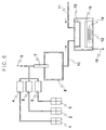
- Fig. 1 is a schematic view showing an arrangement of the CVD apparatus utilizing the vaporizing device for CVD source materials according to a first embodiment of the present invention.
- numerals 1 to 3 denote source material solutions
- numerals 4 to 6 solution supplying means denote source material solutions
- numeral 7 a spray nozzle
- numeral 8 a vaporizer.
- the source material solutions are sprayed into the vaporizer 8 through the spray nozzle 7.
- Numeral 9 denotes a spray gas supplying tube
- numeral 17 is, for instance, a vacuum heat insulating portion serving as a heat insulating mechanism
- numeral 18 a metallic block numeral 19 a cooling device
- numeral 20 a cooling liquid flow path.
- Numeral 21 denotes a heat conduction restricting means wherein the vaporizer 8 and the spray nozzle 7 are fixedly attached to each other through this heat conduction restricting means 21.
- the vaporizing device for CVD source materials comprises the vaporizer 8 having a heating wall surface and the spray nozzle 7 for spraying the CVD source materials, which are either solutions or liquids, into the vaporizer 8 wherein the spray nozzle 7 is cooled through the cooling mechanism and the heat conduction restricting means 21 is provided either at the fixing portion of the spray tip end of the spray nozzle 7 and the vaporizer 8 or proximate to the fixing portion of the spray nozzle or the vaporizer.
- the device of the present embodiment is further configured to thermally insulate the cooled spray nozzle 7 from the vaporizer 8 through the heat insulating mechanism 17.
- numeral 10 denotes a source material gas supply tube, numeral 11 a reaction gas supply tube, numeral 12 a CVD reactor, numeral 13 a CVD gas nozzle, numeral 14 a substrate heating heater, numeral 15 a substrate and numeral 16 exhaust.
- solutions 1 to 3 contained in the source material vessels are sprayed for carburetion by required amounts from the liquid supply vessels 4 to 6 through the spray nozzle 7 into the heated vaporizer 8 together with inert spray gas such as nitrogen, helium or argon from the spray gas supply tube 9.
- the vaporized source materials are sent into the CVD reactor 12 provided with the substrate heating heater 14 by passing through the source material gas supply tube 10 and are intermingled within the CVD gas nozzle 13 with reaction gas which is sent through the reaction (oxide) gas supply tube 11 such that a CVD film (dielectric film) is disposed on the substrate 15.
- the spray nozzle 7 is cooled to assume an arbitrary temperature up to a point located immediately in front of the connecting portion with the vaporizer 8 by means of the cooling mechanism composed of the cooling device 19, cooling liquid flow path 20 and metallic block 18, and the end portion through which the source material solutions are sprayed is fixedly attached to the vaporizer 8 via the heat conduction restricting means 21 so that the spray nozzle 7 is thermally separated from the heated vaporizer 8.
- the spray nozzle 7 can be more reliably thermally separated from the heated vaporizer 8, while the spray nozzle 7 can be thermally separated from the heated vaporizer 8 by means of the heat conduction restricting means 21 also in the absence of the heat insulating mechanism.
- generation of non-vaporized residues and particles within the vaporizing device can be decreased and it is enabled to achieve for improvements in productivity owing to elongation of successive operating time of the vaporizing device and decrease in film forming deficiencies.
- the heat conduction restricting means 21 shall be capable of forming a region which exhibits smaller heat conductivity than the peripheral vaporizer 8 or the main body of the spray nozzle 7.
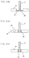
- Fig. 2 is an explanatory view showing an enlarged view of a fixing portion between the vaporizer 8 and the spray nozzle 7 in the present invention wherein 25 denotes a fixing portion in the drawing.
- Fig. 2(a) is a view schematically showing, in an enlarged condition, a portion of Fig. 1 which is provided with the heat conduction restricting means 21 wherein the heat conduction restricting means 21 is exemplified as to be formed of a metallic plate of a small thickness which is thinner than a thickness of walls of metallic portions composing the main body of the vaporizer 8.
- the heat conduction restricting means 21 is, as shown in the drawing, composed of the fixing portion 25 which fixedly attaches the vaporizer 8 with the spray nozzle 7.
- the thickness of the metallic plate of small thickness shall be smaller than the wall thickness of the vaporizer 8 and its approximate thickness shall be not more than approximately 1 mm. Utilization of metal makes it possible to perform welding with the vaporizer or the spray nozzle to thereby provide air-tightness.
- the heat conduction restricting means 21 might be formed of a metallic plate of a small thickness made of e.g. stainless steel, nickel, nickel alloy, platinum or cobalt alloy; or of glass, ceramics, heat-resistant plastics or a combination of these.
- Heat conduction can be restricted by coating at least a part of wall surfaces of the metallic plates of a small thickness with glass, ceramics or heat-resistant plastics, and especially by coating inner walls of the metallic plates of a small thickness, there can be achieved for effects that vaporized gas can be prevented from depositing to be adhered to the metallic plates.
- this notch might function as the heat conduction restricting means 21.
- Fixing of the fixing portion 25 for fixedly attaching the vaporizer 8 and the spray nozzle 7 might be effected by fixing through welding or brazing or by fixing utilizing a gasket.
- the cooling mechanism according to the present invention is composed of a compulsory cooling portion and a heat conduction cooling portion which is in contact with the compulsory cooling portion and the spray nozzle, wherein the cooling means of the compulsory cooling portion performs cooling, besides circulation of cooling liquid, by cooling through a heat pipe, thermoelectric cooling using Peltier elements or cooling by combining these.
- a cooling temperature achieved by the compulsory cooling is so designed that the temperature of source materials in the proximity of the tip end of the spray nozzle is not more than 100 °C, preferably not more than 60 °C. In case this temperature is exceeded, thermal decomposition of source material solutions occur and origomer thereof are formed while deposition occurs in case the temperature is less than a freezing point of the source materials.
- the temperature needs to be set to a temperature with which no deposition in terms of solubility is generated.
- the provision of the heat insulating mechanism for heat-insulating the heated vaporizer and the cooled spray nozzle as shown in Fig. 1 is preferable since it is capable of more reliably maintaining the cooling temperature. It further makes it possible to achieve heating on the side of the vaporizer in an effective manner.
- the heat insulating mechanism might be one which provides heat insulating by using heat-insulating materials besides the above-mentioned heat insulating mechanism through vacuum or a combination of these.
- Fig. 3 is a schematic view showing an arrangement of a CVD apparatus utilizing the vaporizing device for CVD source materials according to a second embodiment of the present invention wherein numeral 23 denotes a spray nozzle of coaxial double tube structure which is composed of an inner tube and an outer tube for making gas containing the CVD source materials and spray gas for spraying these CVD source materials flow in a separate manner.
- numeral 23 denotes a spray nozzle of coaxial double tube structure which is composed of an inner tube and an outer tube for making gas containing the CVD source materials and spray gas for spraying these CVD source materials flow in a separate manner.
- Either one of the gas containing the CVD source materials and the spray gas for spraying these CVD source materials might be made to flow through the inner tube or the outer tube of the spray nozzle 23, and it is also possible to make the CVD source materials and the spray gas respectively flow through the inner tube and the outer tube, and a part of the spray gas might be distributed with the CVD source materials.
- drops of the source material solution to be sprayed into the vaporizer become small and uniform to thereby enable carburetion in an effective and stable manner. Consequently, generation of non-vaporized residues and particles could be decreased and it is enabled to achieve for improvements in productivity owing to elongation of continuous operation time of the vaporizing device and decrease in film forming deficiencies.
- both of the outer tube and the inner tube might be formed of metallic tubes such as stainless steel tubes
- resin exhibiting heat resistant and solvent resistant characteristics such as fluorine group resin, polyimide or polybenzimidazole instead of metal.
- the tip end portion of the inner tube and/or outer tube of the double tube or the tube containing CVD source material gas is formed of the above resin tube, it can be desirably restricted for adhesion of source material solution or reaction thereof.
- the spray nozzle for making gas containing CVD source materials and spray gas for making these CVD source materials flow in a separate manner might also be so arranged that tip end portions of a plurality of tubes for making the respective gases flow in a separate manner are provided proximate to each other to assume an atomizing structure.
- Fig. 4 is a schematic view showing an arrangement of a CVD apparatus utilizing the vaporizing device for CVD source materials according to a third embodiment of the present invention wherein numeral 24 denotes a coating film.
- This coating film might be a coating film of nickel, chrome or oxides thereof, a coating film of an alloy containing nickel or chrome as main components or oxides thereof, a coating film of heat-resistant resin such as fluorine group resin or polyimide group resin, a coating film of holohyaline such as quartz, borosilicate glass, fluorine group glass, phosphate glass or porcelain enamel, or a coating film of ceramics such as alumina (alumite), silicon nitride, aluminum nitride, silicon carbide, titania or titanium nitride, and might also be a film in which either of the above coating film materials are used in combination.
- the provision of the coating film on at least a part of surfaces of the spray nozzle 7 or the vaporizer 8 within the vaporizing device makes it possible to decrease generation of non-vaporized residues and particles on surfaces of materials employed for forming the vaporizing device and to achieve for improvements in productivity owing to elongation of the continuous operation time of the vaporizing device and decrease in film forming deficiencies.
- the thickness of the coating is set to be small and in case it is favorable, the thickness might also be large.
- Embodiments 1 to 3 for instance, by forming the coating film according to the Embodiment 3 on surfaces of the vaporizer and spray nozzle according to the Embodiments 1 and 2, it is enabled to decrease generation of non-vaporized residues and particles and to achieve for improvements in productivity owing to elongation of the continuous operation time of the vaporizing device and decrease in film forming deficiencies.
- Fig. 6 is a schematic view showing an arrangement of a CVD apparatus utilizing a conventional vaporizing device for CVD source materials wherein each of the parts is connected through welding and brazing. It will now be explained for a case in which BST group dielectric films are formed by utilizing the above device.
- Respective source material solutions 1 to 3 of Ba, Sr and Ti each of a density of 0.1 mol/l obtained by dissolving DPM (dipivaloylmethanate) group source materials in THF were sprayed for carburetion through liquid supplying means 4 to 6 by required amounts through the spray nozzle 7 at a flow rate of 1 to 5 ml per minute together with nitrogen gas from the spray gas supply tube 9 (flow rate: 300 CCM) into the vaporizer 8 which has been heated to 200 to 250 °C.
- Portions which are composed of the spray nozzle 7 and the vaporizer 8 form the vaporizing device for CVD source materials.
- Vaporized source material gas was sent into the CVD reactor 12 by passing through the source material gas supply tube 10.
- the source material gas was intermingled within the CVD gas nozzle 13 with reaction gas (oxygen) which has been sent from the reaction (oxide) gas supply tube 11 to form a BST group dielectric film on the substrate 15 disposed on the heating heater 14.
- non-vaporized residues started to be generated upon performing carburetion for approximately 30 minutes in the above vaporizing devices and film deficiencies started to be generated owing to particles which are considered to be due to non-vaporized residues after approximately 60 minutes.
- a stainless steel tube was employed as the spray nozzle 7
- a stainless steel plate of a small thickness having a thickness of approximately 0.5 mm was employed as the heat conduction restricting means 21 (Fig. 2(a))
- heat insulation through vacuum was utilized as the heat-insulating mechanism 17
- an arrangement composed of the compulsory cooling portions 19, 20 utilizing circulation of cooling liquid (water) and of the heat conduction restricting portion provided by the copper metallic block 18 was employed as the cooling mechanism.
- the remaining arrangements were similar to those of Comparative Example 1 and the BST group dielectric film was formed accordingly.
- each of the parts was connected through suitable connecting methods such as welding and brazing.
- the reason why the amount of generated non-vaporized residues could be remarkably reduced in the vaporizing device of the present invention in this manner is considered to be that the source material solutions stay in a cooled state immediately before they are sprayed into the heated vaporizer 8 and the thermal hysteresis applied to the source material solutions at the time of performing carburetion is extremely rapid whereby precursors and origomer of compound oxides that exhibit poor vaporizing characteristics are hardly formed.
- the vaporizing device of the present invention provided with the cooling mechanism for cooling the spray nozzle 7 is more advantaged in that it is capable of restricting evaporation of solution before the carburetion and thus of restricting increases in concentration of the solution before spraying.
- Fig. 5 is a schematic view showing an arrangement of a CVD apparatus including the vaporizing device of the present invention utilizing thermoelectric cooling through Peltier elements 22 instead of the cooling mechanism 19, 20 of Fig. 1.
- numeral 22 denotes Peltier elements by which the metallic block 18 is cooled.
- the CVD source materials are solutions or liquid state materials of Ta alkoxide source materials for Ta oxides, Cu complex source materials for Cu wiring, ferroelectrics of Bi-Sr-Ta group or Pb-Zr-Ti group or other materials of various ceramics, metallic films, metallic oxides, glass or superconductors.
- both inner and outer tubes of the spray nozzle 23 of double tube structure are formed of stainless steel tubes wherein CVD source materials are made to flow through the inner tube and spray gas for spraying the CVD source materials through the outer tube.
- a thin stainless steel plate having a thickness of approximately 0.5 mm was employed as the heat conduction restricting means 21 similarly to that of Example 1, a foam fluoride resin group heat insulating material was utilized as the heat-insulating mechanism 17, and an arrangement composed of the compulsory cooling portions 19, 20 utilizing circulation of cooling liquid (water) and of the heat conduction restricting portion provided by a stainless steel metallic block was employed as the cooling mechanism. Connection of each of the parts was performed through suitable connecting methods such as welding and brazing.
- a Ru solution of a concentration of 0.1 mol/l as a source material solution 1 obtained by dissolving a DPM group source material in THF at a flow rate of 5 ml per minute was performed at a cooling temperature of 5 to 20°C for the nozzle, a flow rate of 150 ccm for the spray gas (argon), a flow rate of 1,000 CCM for the reaction gas (hydrogen) and a vaporizing temperature of 180 to 200°C to perform vaporizing tests for 300 minutes and film forming tests during the same period similarly to the case of Example 1.
- productivity of final semiconductor memories including Ru electrode films or electronic parts could be improved owing to elongation of continuous operation time of the vaporizer.
- the reason why the amount of generated non-vaporized residues could be reduced in the vaporizing device employing a spray nozzle of double tube structure according to the present invention is considered to be due to the fact that an atomizing structure was formed at the tip end portion through the double tube structure whereby drops of the source material solution to be sprayed became small and uniform, and that a spraying area with respect to the vaporizer was increased to enable carburetion in a more effective manner.
- productivity of final semiconductor memories including Cu electrode films or electronic parts could be improved owing to elongation of continuous operation time of the vaporizer.
- a PZT group dielectric film was formed using the CVD apparatus with a nickel coating having a thickness of 20 to 100 ⁇ m as the coating film 24 on inner surfaces of the vaporizer 8.
- the material for the vaporizer 8 was stainless steel and the spray nozzle 7 was formed of a Teflon tube.
- the amount of generated non-vaporized residues within the vaporizer could be decreased to approximately half of the amount in case no nickel coating film 24 was provided, so that elongation of continuous operation time of the vaporizing device could be achieved.
- the reason why the amount of generated non-vaporized residues could be reduced in the vaporizing device of the illustrated example is considered to be due to the face that the surface of the stainless steel promotes decomposition of source materials while the extent of decomposition by nickel is small.
- While the illustrated example is related to a case employing a nickel coating film, similar effects might be obtained by utilizing a coating film of chrome, a coating film of an oxide of nickel or chrome, a coating film of an alloy containing nickel or chrome as a main component or of an oxide of these, a coating film of heat-resistant resin, a coating film of holohyaline, or a coating film of ceramics.
- a CVD vaporizing device obtained by combining those of the above Examples 1 to 3 was used.
- the spray nozzle 7 of Fig. 1 was replaced by the spray nozzle 23 of Example 2 (Fig. 3), and a coating film 24 was formed on the inner surface of the vaporizer 8 (Fig. 4) and a coating film of chrome oxide layer on the inner surface of the spray nozzle 23 (not shown).
- the CVD source material solutions were made to flow through the inner tube and spray gas through both the outer tube and the inner tube, and the flow rate of spray gas (nitrogen) was set to be 200 CCM, respectively.
- Carburetion of the respective source materials of a flow rate of 0.1 to 5 ml per minute was performed at a cooling temperature of 5 to 20°C for the spray nozzle and a vaporizing temperature of 200 to 250°C to perform vaporizing tests for 300 minutes and film forming tests during the same period, similarly to Example 1.
- a first vaporizing device for CVD source materials comprises a vaporizer for vaporizing introduced CVD source materials through heating, a spray nozzle of which end portion is fixedly attached to the vaporizer for spraying the CVD materials into the vaporizer, a cooling mechanism for cooling the spray nozzle, and a heat conduction restricting means which is attached either to the fixing portion, or to a portion of the spray nozzle or the vaporizer proximate of the fixing portion.
- a second vaporizing device for CVD source materials according to the present invention is so arranged that the first vaporizing device for CVD source materials further includes a heat insulating mechanism for thermally insulating the vaporizer from the cooled spray nozzle.
- a third vaporizing device for CVD source materials according to the present invention is so arranged that in the first or second vaporizing device for CVD source materials, the heat conduction restricting means is configured to assume a wall thickness which is smaller than a wall thickness of the vaporizer or the spray nozzle disposed in a periphery of the heat conduction restricting means.
- a fourth vaporizing device for CVD source materials according to the present invention is so arranged that in the third vaporizing device for CVD source materials, the heat conduction restricting means is formed of a metallic plate of which thickness is smaller than the wall thickness of the vaporizer.
- a fifth vaporizing device for CVD source materials according to the present invention is so arranged that in the fourth vaporizing device for CVD source materials, a wall surface of the metallic plate of a small thickness is covered with glass, ceramics or heat-resisting plastics.
- a sixth vaporizing device for CVD source materials according to the present invention is so arranged that in either one of the first to fifth vaporizing devices for CVD source materials, the spray nozzle is configured to make gas containing the CVD source materials and spray gas for spraying the CVD source materials flow in a separate manner.
- a seventh vaporizing device for CVD source materials according to the present invention is so arranged that in the sixth vaporizing device for CVD source materials, the spray nozzle is formed as a double tube structure composed of an inner tube and an outer tube wherein gas containing the CVD source materials is made to flow through one of the tubes and spray gas for spraying the CVD source materials is made to flow through the other one of the tubes.
- An eighth vaporizing device for CVD source materials according to the present invention is so arranged that in the seventh vaporizing device for CVD source materials, the double tube is made of metal, resin or a complex of these. With this arrangement, there can be achieved for an effect that generation of non-vaporized residues and particles can be further decreased and that improvements in productivity owing to elongation of continuous operation time and decrease in film forming deficiencies can be achieved.
- a ninth vaporizing device for CVD source materials according to the present invention is so arranged that in the eighth vaporizing device for CVD source materials, either a tip end portion of the double tube or the tube through which the CVD source material is made to flow is formed of resin.
- a tenth vaporizing device for CVD source materials according to the present invention is so arranged that in the eighth vaporizing device for CVD source materials, the outer tube of the double tube is formed of metal.
- the tube can be manufactured easily, and there can be achieved for an effect that generation of non-vaporized residues and particles can be further decreased and that improvements in productivity owing to elongation of continuous operation time and decrease in film forming deficiencies can be achieved.
- An eleventh vaporizing device for CVD source materials according to the present invention is so arranged that in either one of the eighth to tenth vaporizing devices for CVD source materials, the resin is fluorine group resin, polyimide or polybenzimidazole. With this arrangement, there can be achieved for an effect that generation of non-vaporized residues and particles can be further decreased and that improvements in productivity owing to elongation of continuous operation time and decrease in film forming deficiencies can be achieved.
- a twelfth vaporizing device for CVD source materials is so arranged that in either one of the first to seventh vaporizing devices for CVD source materials, surfaces of inner walls of the spray nozzle or the inner walls of the vaporizer are formed with a coating film of nickel, chrome or an oxide thereof, a coating film of an alloy including as main components nickel or chrome or an oxide thereof, a coating film of heat-resisting resin, a coating film of holohyaline, or a coating film of ceramics.
- a thirteenth vaporizing device for CVD source materials is so arranged that in a vaporizing device for CVD source materials comprising a vaporizer for vaporizing introduced CVD source materials through heating and a spray nozzle for spraying the CVD materials into the vaporizer, surfaces of inner walls of the spray nozzle or the inner walls of the vaporizer are formed with a coating film of nickel, chrome or an oxide thereof, a coating film of an alloy including as main components nickel or chrome or an oxide thereof, a coating film of heat-resisting resin, a coating film of holohyaline, or a coating film of ceramics.
- a CVD apparatus comprises any one of the above first to thirteenth vaporizing devices for CVD source materials, a supply portion for supplying the CVD source materials into the vaporizing device for CVD source materials and a reacting portion for forming a layer on a substrate through reaction of the source materials which have been vaporized by the vaporizing device for CVD source materials.
Landscapes
- Chemical & Material Sciences (AREA)
- General Chemical & Material Sciences (AREA)
- Chemical Kinetics & Catalysis (AREA)
- Engineering & Computer Science (AREA)
- Materials Engineering (AREA)
- Mechanical Engineering (AREA)
- Metallurgy (AREA)
- Organic Chemistry (AREA)
- Dispersion Chemistry (AREA)
- Chemical Vapour Deposition (AREA)
- Feeding, Discharge, Calcimining, Fusing, And Gas-Generation Devices (AREA)
Abstract
Description
Claims (10)
- A vaporizing device for CVD source materials comprisinga vaporizer (8) for vaporizing introduced CVD source materials through heating,a spray nozzle (7) the end portion of which is fixedly attached to the vaporizer (8) for spraying the CVD source materials into the vaporizer (8),a cooling mechanism (19, 20) for cooling the spray nozzle (7), andheat conduction restricting means (21) attached either to a fixing portion (25), or provided proximate to a fixing portion (25) of the spray nozzle (7) or the vaporizer (8).
- The device according to claim 1,
wherein the device further includes a heat insulating mechanism (17) for thermally insulating the vaporizer (8) from the cooled spray nozzle (7). - The device according to claim 1 or 2,
wherein the heat conduction restricting means (21) are formed of a metallic plate the thickness of which is smaller than the wall thickness of the vaporizer (8). - The device according to claim 3,
wherein at least a part of a wall surface of the metallic plate (21) of a small thickness is covered by glass, ceramics or heat-resisting plastics. - The device according to any of claims 1 to 4,
wherein the spray nozzle (7, 23) is a nozzle which is configured to make a gas containing the CVD source materials and a spray gas for spraying the CVD source materials flow in a separate manner. - The device according to claim 5,
wherein the spray nozzle (23) is formed as a coaxial double tube structure composed of an inner tube and an outer tube, and
wherein the gas containing the CVD source materials is made to flow through one of the tubes and the spray gas for spraying the CVD source materials is made to flow through the other one of the tubes. - The device according to claim 6,
wherein the coaxial double tube is made of metal, resin or a complex of these. - The device according to claim 6 or 7,
wherein either a tip end portion of an inner tube and/or an outer tube of the coaxial double tube or the tube through which the CVD source material is made to flow is formed of resin. - The device according to claim 7,
wherein the outer tube of the coaxial double tube is formed of metal. - A CVD apparatus comprising:(a) a vaporizing device for CVD source materials comprisinga vaporizer (8) for vaporizing introduced CVD source materials through heating,a spray nozzle (7) the end portion of which is fixedly attached to the vaporizer (8) for spraying the CVD source materials into the vaporizer (8),a cooling mechanism (19, 20) for cooling the spray nozzle (7),heat conduction restricting means (21) attached either to a fixing portion (25), or provided proximate to a fixing portion (25) of the spray nozzle (7) or the vaporizer (8), anda heat insulating mechanism (17) for thermally insulating the vaporizer (8) from the cooled spray nozzle (7);(b) a supply portion (1-6) for supplying the CVD source materials into the vaporizing device for CVD source materials; and(c) a reacting portion (12) for forming a film on a substrate (15) through reaction of the source materials which have been vaporized by the vaporizing device for CVD source materials.
Applications Claiming Priority (2)
| Application Number | Priority Date | Filing Date | Title |
|---|---|---|---|
| JP08149999A JP3823591B2 (en) | 1999-03-25 | 1999-03-25 | Vaporizing apparatus for CVD raw material and CVD apparatus using the same |
| JP8149999 | 1999-03-25 |
Publications (3)
| Publication Number | Publication Date |
|---|---|
| EP1038988A2 true EP1038988A2 (en) | 2000-09-27 |
| EP1038988A3 EP1038988A3 (en) | 2003-01-29 |
| EP1038988B1 EP1038988B1 (en) | 2009-05-13 |
Family
ID=13748077
Family Applications (1)
| Application Number | Title | Priority Date | Filing Date |
|---|---|---|---|
| EP00106247A Expired - Lifetime EP1038988B1 (en) | 1999-03-25 | 2000-03-22 | Vaporizing device for CVD apparatus |
Country Status (6)
| Country | Link |
|---|---|
| US (2) | US6273957B1 (en) |
| EP (1) | EP1038988B1 (en) |
| JP (1) | JP3823591B2 (en) |
| KR (1) | KR100377707B1 (en) |
| DE (1) | DE60042181D1 (en) |
| TW (1) | TW486524B (en) |
Cited By (8)
| Publication number | Priority date | Publication date | Assignee | Title |
|---|---|---|---|---|
| WO2002040739A1 (en) * | 2000-11-20 | 2002-05-23 | Aixtron Ag | Device and method for supplying a cvd reactor with a liquid starting material entering into a gaseous phase |
| EP1211333A3 (en) * | 2000-12-01 | 2003-07-30 | Japan Pionics Co., Ltd. | Vaporizer for CVD apparatus |
| EP1473384A1 (en) * | 2003-05-01 | 2004-11-03 | Japan Pionics Co., Ltd. | Vaporizer |
| WO2005026401A3 (en) * | 2003-09-17 | 2005-06-09 | Aixtron Ag | Method and device for depositing layers using non-continuous injection |
| US7027561B2 (en) | 2003-04-16 | 2006-04-11 | Xcounter Ab | Dual-energy scanning-based detection of ionizing radiation |
| US7732308B2 (en) | 2003-09-17 | 2010-06-08 | Aixtron, Inc. | Process for depositing layers containing silicon and germanium |
| US8584965B2 (en) | 2006-04-19 | 2013-11-19 | Kemstream | Device for introducing, injecting or spraying a mixture of a carrier gas and liquid compounds and method for implementing said device |
| CN107431015A (en) * | 2015-11-10 | 2017-12-01 | 东京毅力科创株式会社 | Gasifier, film forming device and temperature control method |
Families Citing this family (26)
| Publication number | Priority date | Publication date | Assignee | Title |
|---|---|---|---|---|
| US7163197B2 (en) * | 2000-09-26 | 2007-01-16 | Shimadzu Corporation | Liquid substance supply device for vaporizing system, vaporizer, and vaporization performance appraisal method |
| US7246796B2 (en) | 2001-01-18 | 2007-07-24 | Masayuki Toda | Carburetor, various types of devices using the carburetor, and method of vaporization |
| JP2002313781A (en) * | 2001-04-11 | 2002-10-25 | Sumitomo Electric Ind Ltd | Substrate processing equipment |
| KR20030050941A (en) * | 2001-12-20 | 2003-06-25 | 주성엔지니어링(주) | Vaporizer which can prevent clogging |
| JP3778851B2 (en) * | 2001-12-25 | 2006-05-24 | Smc株式会社 | Poppet valve with heater |
| US6758591B1 (en) | 2002-03-22 | 2004-07-06 | Novellus Systems, Inc. | Mixing of materials in an integrated circuit manufacturing equipment |
| JP4259203B2 (en) * | 2002-10-29 | 2009-04-30 | トヨタ自動車株式会社 | Fuel reformer and fuel cell system |
| US6997403B2 (en) * | 2003-01-13 | 2006-02-14 | Micron Technology, Inc. | Liquid vaporizer with positive liquid shut-off |
| US7067458B2 (en) * | 2003-02-26 | 2006-06-27 | Tdk Corporation | Multi-layered unit including electrode and dielectric layer |
| US20060237760A1 (en) * | 2003-02-27 | 2006-10-26 | Tdk Corporation | Thin-film capacitative element and electronic circuit and electronic equipment including the same |
| US20050194098A1 (en) * | 2003-03-24 | 2005-09-08 | Advanced Energy Industries, Inc. | Cast design for plasma chamber cooling |
| US20050271893A1 (en) * | 2004-06-04 | 2005-12-08 | Applied Microstructures, Inc. | Controlled vapor deposition of multilayered coatings adhered by an oxide layer |
| JP2005133157A (en) * | 2003-10-30 | 2005-05-26 | Watanabe Shoko:Kk | Organometal chemical vapor deposition apparatus |
| JP4607474B2 (en) * | 2004-02-12 | 2011-01-05 | 東京エレクトロン株式会社 | Deposition equipment |
| JP5265583B2 (en) * | 2008-02-14 | 2013-08-14 | 株式会社アルバック | Vapor deposition equipment |
| JP2010087169A (en) * | 2008-09-30 | 2010-04-15 | Tokyo Electron Ltd | Carburetor and film-forming system using the same |
| JP5416570B2 (en) * | 2009-12-15 | 2014-02-12 | 住友電気工業株式会社 | Heating / cooling device and apparatus equipped with the same |
| EP2369033A1 (en) * | 2010-03-26 | 2011-09-28 | Saint-Gobain Glass France | Method for refilling an evaporation chamber |
| US9861610B2 (en) | 2011-08-01 | 2018-01-09 | Akay Flavours & Aromatics Pvt Ltd. | Process for selective extraction of bioactive and bioavailable cinnamon polyphenols and procyanidin oligomers and a stable composition thereof |
| WO2013094680A1 (en) * | 2011-12-20 | 2013-06-27 | 株式会社日立国際電気 | Substrate processing device, method for manufacturing semiconductor device, and vaporizer |
| US8778081B2 (en) * | 2012-01-04 | 2014-07-15 | Colorado State University Research Foundation | Process and hardware for deposition of complex thin-film alloys over large areas |
| KR102269079B1 (en) * | 2015-05-08 | 2021-06-25 | (주)지오엘리먼트 | vaporizer |
| KR101725959B1 (en) * | 2015-05-08 | 2017-04-21 | (주)지오엘리먼트 | vaporizer |
| WO2017163375A1 (en) * | 2016-03-24 | 2017-09-28 | 株式会社日立国際電気 | Vaporizer, substrate treatment apparatus, and method for manufacturing semiconductor device |
| JP6907406B2 (en) * | 2018-03-23 | 2021-07-21 | 株式会社Kokusai Electric | Manufacturing method of vaporizer, substrate processing equipment and semiconductor equipment |
| EP4678785A1 (en) * | 2023-03-07 | 2026-01-14 | Shin-Etsu Chemical Co., Ltd. | Film formation nozzle and film formation device |
Family Cites Families (14)
| Publication number | Priority date | Publication date | Assignee | Title |
|---|---|---|---|---|
| US4219725A (en) * | 1978-08-01 | 1980-08-26 | The Dow Chemical Company | Heating apparatus for vaporizing liquefied gases |
| DE3513307A1 (en) * | 1985-04-13 | 1986-10-16 | Henkel KGaA, 4000 Düsseldorf | ELECTRICAL DEVICE FOR EVAPORATING INSECTICIDAL ACTIVE SUBSTANCE |
| JPS621870A (en) * | 1985-06-25 | 1987-01-07 | Nec Corp | Vapor depositing apparatus |
| DE4041623A1 (en) * | 1990-12-22 | 1992-06-25 | Osu Maschinenbau Gmbh | NOZZLE FOR A DEVICE AND A METHOD FOR HIGH-SPEED FLAME SPRAYING |
| JPH06291040A (en) * | 1992-03-03 | 1994-10-18 | Rintetsuku:Kk | Method and apparatus for vaporizing and supplying liquid |
| JP3720083B2 (en) | 1995-07-21 | 2005-11-24 | 株式会社日立製作所 | Method and apparatus for manufacturing thin film for semiconductor element, and semiconductor wafer |
| JP3276277B2 (en) * | 1995-11-29 | 2002-04-22 | 株式会社フジクラ | Liquid material supply device for CVD |
| US5835677A (en) * | 1996-10-03 | 1998-11-10 | Emcore Corporation | Liquid vaporizer system and method |
| US5835678A (en) * | 1996-10-03 | 1998-11-10 | Emcore Corporation | Liquid vaporizer system and method |
| US6074487A (en) * | 1997-02-13 | 2000-06-13 | Shimadzu Corporation | Unit for vaporizing liquid materials |
| JP3645682B2 (en) | 1997-03-18 | 2005-05-11 | 三菱電機株式会社 | CVD equipment for Cu film formation |
| US6157774A (en) * | 1997-05-16 | 2000-12-05 | Tokyo Electron Limited | Vapor generating method and apparatus using same |
| US6210485B1 (en) * | 1998-07-21 | 2001-04-03 | Applied Materials, Inc. | Chemical vapor deposition vaporizer |
| GB9900955D0 (en) * | 1999-01-15 | 1999-03-10 | Imperial College | Material deposition |
-
1999
- 1999-03-25 JP JP08149999A patent/JP3823591B2/en not_active Expired - Fee Related
-
2000
- 2000-03-20 TW TW089105033A patent/TW486524B/en not_active IP Right Cessation
- 2000-03-22 EP EP00106247A patent/EP1038988B1/en not_active Expired - Lifetime
- 2000-03-22 DE DE60042181T patent/DE60042181D1/en not_active Expired - Lifetime
- 2000-03-23 US US09/532,446 patent/US6273957B1/en not_active Expired - Lifetime
- 2000-03-24 KR KR10-2000-0015015A patent/KR100377707B1/en not_active Expired - Fee Related
-
2001
- 2001-07-06 US US09/899,183 patent/US20010039923A1/en not_active Abandoned
Cited By (11)
| Publication number | Priority date | Publication date | Assignee | Title |
|---|---|---|---|---|
| WO2002040739A1 (en) * | 2000-11-20 | 2002-05-23 | Aixtron Ag | Device and method for supplying a cvd reactor with a liquid starting material entering into a gaseous phase |
| EP1211333A3 (en) * | 2000-12-01 | 2003-07-30 | Japan Pionics Co., Ltd. | Vaporizer for CVD apparatus |
| KR100865423B1 (en) * | 2000-12-01 | 2008-10-24 | 니뽄파이오닉스가부시끼가이샤 | Vaporizer and apparatus for vaporizing and supplying |
| US7027561B2 (en) | 2003-04-16 | 2006-04-11 | Xcounter Ab | Dual-energy scanning-based detection of ionizing radiation |
| EP1473384A1 (en) * | 2003-05-01 | 2004-11-03 | Japan Pionics Co., Ltd. | Vaporizer |
| WO2005026401A3 (en) * | 2003-09-17 | 2005-06-09 | Aixtron Ag | Method and device for depositing layers using non-continuous injection |
| US7410670B2 (en) | 2003-09-17 | 2008-08-12 | Aixtron Ag | Process and apparatus for depositing single-component or multi-component layers and layer sequences using discontinuous injection of liquid and dissolved starting substances via a multi-channel injection unit |
| US7732308B2 (en) | 2003-09-17 | 2010-06-08 | Aixtron, Inc. | Process for depositing layers containing silicon and germanium |
| US8584965B2 (en) | 2006-04-19 | 2013-11-19 | Kemstream | Device for introducing, injecting or spraying a mixture of a carrier gas and liquid compounds and method for implementing said device |
| US9387447B2 (en) | 2006-04-19 | 2016-07-12 | Kemstream | Device for introducing, injecting or spraying a mixture of a carrier gas and liquid compounds and method for implementing said device |
| CN107431015A (en) * | 2015-11-10 | 2017-12-01 | 东京毅力科创株式会社 | Gasifier, film forming device and temperature control method |
Also Published As
| Publication number | Publication date |
|---|---|
| TW486524B (en) | 2002-05-11 |
| EP1038988A3 (en) | 2003-01-29 |
| JP2000273639A (en) | 2000-10-03 |
| US6273957B1 (en) | 2001-08-14 |
| KR20000076945A (en) | 2000-12-26 |
| US20010039923A1 (en) | 2001-11-15 |
| JP3823591B2 (en) | 2006-09-20 |
| EP1038988B1 (en) | 2009-05-13 |
| KR100377707B1 (en) | 2003-03-26 |
| DE60042181D1 (en) | 2009-06-25 |
Similar Documents
| Publication | Publication Date | Title |
|---|---|---|
| EP1038988B1 (en) | Vaporizing device for CVD apparatus | |
| US6470144B1 (en) | Vaporizer for chemical vapor deposition apparatus, chemical vapor deposition apparatus, and semiconductor device manufactured thereby | |
| JP3390517B2 (en) | Liquid source CVD equipment | |
| JP4220075B2 (en) | Film forming method and film forming apparatus | |
| JP3612839B2 (en) | High dielectric constant thin film structure, high dielectric constant thin film forming method, and high dielectric constant thin film forming apparatus | |
| US6110283A (en) | Chemical vapor deposition apparatus | |
| KR100297210B1 (en) | High Temperature Electrode-Barriers for Ferroelectric Capacitors and Other Capacitor Structures | |
| US8816447B2 (en) | Transistor with reduced depletion field width | |
| US6943073B2 (en) | Process for low temperature atomic layer deposition of RH | |
| JPH11297681A (en) | CVD apparatus for forming high dielectric constant thin film and method for forming high dielectric constant thin film | |
| US5686151A (en) | Method of forming a metal oxide film | |
| TW201139721A (en) | Thin film manufacturing apparatus, thin film manufacturing method, and method for manufacturing semiconductor device | |
| US7071053B2 (en) | Method of forming capacitor with ruthenium top and bottom electrodes by MOCVD | |
| KR20020042228A (en) | Formation system and method for Sr-Ta-O thin films | |
| US7291530B2 (en) | Semiconductor storage device and method of manufacturing the same | |
| US6812510B2 (en) | Ferroelectric capacitor, process for manufacturing thereof and ferroelectric memory | |
| US6640403B2 (en) | Method for forming a dielectric-constant-enchanced capacitor | |
| US6297122B1 (en) | Method of forming conductive film and capacitor | |
| JPH11236675A (en) | Thin film forming apparatus and thin film forming method | |
| JP3111994B2 (en) | Vapor growth apparatus for metal oxide dielectric materials | |
| JPH09241849A (en) | Oxide thin film manufacturing apparatus and manufacturing method thereof | |
| US6461910B1 (en) | Method of forming a capacitor in a semiconductor device | |
| JP2002305194A (en) | Metal oxide thin film forming method and film forming apparatus | |
| JP3353835B2 (en) | Vapor phase growth method of metal oxide dielectric film | |
| GB2358085A (en) | Method of forming a capacitor with crystalline tantalum oxide nitride TaON dielectric layer by LPCVD |
Legal Events
| Date | Code | Title | Description |
|---|---|---|---|
| PUAI | Public reference made under article 153(3) epc to a published international application that has entered the european phase |
Free format text: ORIGINAL CODE: 0009012 |
|
| AK | Designated contracting states |
Kind code of ref document: A2 Designated state(s): AT BE CH CY DE DK ES FI FR GB GR IE IT LI LU MC NL PT SE |
|
| AX | Request for extension of the european patent |
Free format text: AL;LT;LV;MK;RO;SI |
|
| PUAL | Search report despatched |
Free format text: ORIGINAL CODE: 0009013 |
|
| AK | Designated contracting states |
Designated state(s): AT BE CH CY DE DK ES FI FR GB GR IE IT LI LU MC NL PT SE |
|
| AX | Request for extension of the european patent |
Extension state: AL LT LV MK RO SI |
|
| RIC1 | Information provided on ipc code assigned before grant |
Ipc: 7C 23C 16/44 A Ipc: 7B 05B 1/00 B Ipc: 7C 23C 16/448 B |
|
| RIN1 | Information on inventor provided before grant (corrected) |
Inventor name: TARUTANI,MASAYOSHI,C/O MITSUBISHI DENKI K.K. Inventor name: KAWAHARA,TAKAAKI,C/O MITSUBISHI DENKI K.K. Inventor name: YAMAMUKA,MIKIO,C/O MITSUBISHI DENKI K.K. Inventor name: UCHIKAWA, FUSAOKI,C/O MITSUBISHI DENKI K.K. Inventor name: MATSUNO,SHIGERU,C/O MITSUBISHI DENKI K.K. Inventor name: SATO,TAKEHIKO,C/O MITSUBISHI DENKI K.K. Inventor name: HORIKAWA,TSUYOSHI,C/O MITSUBISHI DENKI K.K. Inventor name: YAMADA,AKIRA ,C/O MITSUBISHI DENKI K.K. |
|
| 17P | Request for examination filed |
Effective date: 20030404 |
|
| AKX | Designation fees paid |
Designated state(s): DE FR NL |
|
| RAP1 | Party data changed (applicant data changed or rights of an application transferred) |
Owner name: MITSUBISHI DENKI KABUSHIKI KAISHA |
|
| 17Q | First examination report despatched |
Effective date: 20071127 |
|
| GRAP | Despatch of communication of intention to grant a patent |
Free format text: ORIGINAL CODE: EPIDOSNIGR1 |
|
| GRAS | Grant fee paid |
Free format text: ORIGINAL CODE: EPIDOSNIGR3 |
|
| GRAA | (expected) grant |
Free format text: ORIGINAL CODE: 0009210 |
|
| AK | Designated contracting states |
Kind code of ref document: B1 Designated state(s): DE FR NL |
|
| REF | Corresponds to: |
Ref document number: 60042181 Country of ref document: DE Date of ref document: 20090625 Kind code of ref document: P |
|
| NLV1 | Nl: lapsed or annulled due to failure to fulfill the requirements of art. 29p and 29m of the patents act | ||
| PG25 | Lapsed in a contracting state [announced via postgrant information from national office to epo] |
Ref country code: NL Free format text: LAPSE BECAUSE OF FAILURE TO SUBMIT A TRANSLATION OF THE DESCRIPTION OR TO PAY THE FEE WITHIN THE PRESCRIBED TIME-LIMIT Effective date: 20090513 |
|
| PLBE | No opposition filed within time limit |
Free format text: ORIGINAL CODE: 0009261 |
|
| STAA | Information on the status of an ep patent application or granted ep patent |
Free format text: STATUS: NO OPPOSITION FILED WITHIN TIME LIMIT |
|
| 26N | No opposition filed |
Effective date: 20100216 |
|
| REG | Reference to a national code |
Ref country code: FR Ref legal event code: ST Effective date: 20101130 |
|
| PG25 | Lapsed in a contracting state [announced via postgrant information from national office to epo] |
Ref country code: FR Free format text: LAPSE BECAUSE OF NON-PAYMENT OF DUE FEES Effective date: 20100331 |
|
| REG | Reference to a national code |
Ref country code: DE Ref legal event code: R084 Ref document number: 60042181 Country of ref document: DE Effective date: 20120425 |
|
| PGFP | Annual fee paid to national office [announced via postgrant information from national office to epo] |
Ref country code: DE Payment date: 20170314 Year of fee payment: 18 |
|
| REG | Reference to a national code |
Ref country code: DE Ref legal event code: R119 Ref document number: 60042181 Country of ref document: DE |
|
| PG25 | Lapsed in a contracting state [announced via postgrant information from national office to epo] |
Ref country code: DE Free format text: LAPSE BECAUSE OF NON-PAYMENT OF DUE FEES Effective date: 20181002 |