EP1037341B1 - Optically pumped VCSEL - Google Patents
Optically pumped VCSEL Download PDFInfo
- Publication number
- EP1037341B1 EP1037341B1 EP00102463A EP00102463A EP1037341B1 EP 1037341 B1 EP1037341 B1 EP 1037341B1 EP 00102463 A EP00102463 A EP 00102463A EP 00102463 A EP00102463 A EP 00102463A EP 1037341 B1 EP1037341 B1 EP 1037341B1
- Authority
- EP
- European Patent Office
- Prior art keywords
- light
- wavelength
- vcsel
- substrate
- layer stack
- Prior art date
- Legal status (The legal status is an assumption and is not a legal conclusion. Google has not performed a legal analysis and makes no representation as to the accuracy of the status listed.)
- Expired - Lifetime
Links
Images

Classifications
-
- H—ELECTRICITY
- H01—ELECTRIC ELEMENTS
- H01S—DEVICES USING THE PROCESS OF LIGHT AMPLIFICATION BY STIMULATED EMISSION OF RADIATION [LASER] TO AMPLIFY OR GENERATE LIGHT; DEVICES USING STIMULATED EMISSION OF ELECTROMAGNETIC RADIATION IN WAVE RANGES OTHER THAN OPTICAL
- H01S5/00—Semiconductor lasers
- H01S5/40—Arrangement of two or more semiconductor lasers, not provided for in groups H01S5/02 - H01S5/30
- H01S5/42—Arrays of surface emitting lasers
- H01S5/423—Arrays of surface emitting lasers having a vertical cavity
- H01S5/426—Vertically stacked cavities
-
- H—ELECTRICITY
- H01—ELECTRIC ELEMENTS
- H01S—DEVICES USING THE PROCESS OF LIGHT AMPLIFICATION BY STIMULATED EMISSION OF RADIATION [LASER] TO AMPLIFY OR GENERATE LIGHT; DEVICES USING STIMULATED EMISSION OF ELECTROMAGNETIC RADIATION IN WAVE RANGES OTHER THAN OPTICAL
- H01S5/00—Semiconductor lasers
- H01S5/02—Structural details or components not essential to laser action
- H01S5/0206—Substrates, e.g. growth, shape, material, removal or bonding
- H01S5/0215—Bonding to the substrate
- H01S5/0216—Bonding to the substrate using an intermediate compound, e.g. a glue or solder
-
- H—ELECTRICITY
- H01—ELECTRIC ELEMENTS
- H01S—DEVICES USING THE PROCESS OF LIGHT AMPLIFICATION BY STIMULATED EMISSION OF RADIATION [LASER] TO AMPLIFY OR GENERATE LIGHT; DEVICES USING STIMULATED EMISSION OF ELECTROMAGNETIC RADIATION IN WAVE RANGES OTHER THAN OPTICAL
- H01S5/00—Semiconductor lasers
- H01S5/04—Processes or apparatus for excitation, e.g. pumping, e.g. by electron beams
- H01S5/041—Optical pumping
-
- H—ELECTRICITY
- H01—ELECTRIC ELEMENTS
- H01S—DEVICES USING THE PROCESS OF LIGHT AMPLIFICATION BY STIMULATED EMISSION OF RADIATION [LASER] TO AMPLIFY OR GENERATE LIGHT; DEVICES USING STIMULATED EMISSION OF ELECTROMAGNETIC RADIATION IN WAVE RANGES OTHER THAN OPTICAL
- H01S5/00—Semiconductor lasers
- H01S5/10—Construction or shape of the optical resonator, e.g. extended or external cavity, coupled cavities, bent-guide, varying width, thickness or composition of the active region
- H01S5/18—Surface-emitting [SE] lasers, e.g. having both horizontal and vertical cavities
- H01S5/183—Surface-emitting [SE] lasers, e.g. having both horizontal and vertical cavities having only vertical cavities, e.g. vertical cavity surface-emitting lasers [VCSEL]
- H01S5/18308—Surface-emitting [SE] lasers, e.g. having both horizontal and vertical cavities having only vertical cavities, e.g. vertical cavity surface-emitting lasers [VCSEL] having a special structure for lateral current or light confinement
- H01S5/18311—Surface-emitting [SE] lasers, e.g. having both horizontal and vertical cavities having only vertical cavities, e.g. vertical cavity surface-emitting lasers [VCSEL] having a special structure for lateral current or light confinement using selective oxidation
-
- H—ELECTRICITY
- H01—ELECTRIC ELEMENTS
- H01S—DEVICES USING THE PROCESS OF LIGHT AMPLIFICATION BY STIMULATED EMISSION OF RADIATION [LASER] TO AMPLIFY OR GENERATE LIGHT; DEVICES USING STIMULATED EMISSION OF ELECTROMAGNETIC RADIATION IN WAVE RANGES OTHER THAN OPTICAL
- H01S5/00—Semiconductor lasers
- H01S5/10—Construction or shape of the optical resonator, e.g. extended or external cavity, coupled cavities, bent-guide, varying width, thickness or composition of the active region
- H01S5/18—Surface-emitting [SE] lasers, e.g. having both horizontal and vertical cavities
- H01S5/183—Surface-emitting [SE] lasers, e.g. having both horizontal and vertical cavities having only vertical cavities, e.g. vertical cavity surface-emitting lasers [VCSEL]
- H01S5/18361—Structure of the reflectors, e.g. hybrid mirrors
- H01S5/18369—Structure of the reflectors, e.g. hybrid mirrors based on dielectric materials
Definitions
- the invention relates generally to vertical-cavity surface-emitting lasers and more particularly to an optically pumped vertical-cavity surface-emitting laser.
- VCSELs Vertical-cavity surface-emitting lasers
- edge-emitting lasers such as low manufacturing cost, good beam quality and scalable geometries. These properties make VCSELs desirable for many applications.
- VCSELs that can produce long wavelength light (1300 nm-1550 nm) are of interest in optical communications.
- a VCSEL may be driven by electrical current or may be optically pumped to produce the output laser light.
- a conventional current-injection VCSEL includes an active region that is positioned between two distributed Bragg reflectors (DBRs) that are formed on a substrate.
- the current-injection VCSEL includes two ohmic contacts for applying electrical current to the active region. Typically, one of the ohmic contacts is located below the substrate, while the other ohmic contact is located above the top DBR.
- electrical current is injected into the active region, causing the active region to emit light. The emitted light is reflected between the two DBRs. A portion of the emitted light may propagate through the top DBR or the bottom DBR as the output laser light.
- a conventional optically pumped VCSEL also includes an active region between two DBRs.
- the optically pumped VCSEL includes, or is operationally associated with, a light source.
- the light source may be another VCSEL or a light-emitting diode.
- the optically pumped VCSEL generates the output laser light by absorbing "pump light" supplied by the . light source. The pump light is absorbed by the active region, which causes emission of the output laser light.
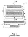
- U.S. Pat. No. 5,513,204 to Jayaraman describes an optically pumped VCSEL device that includes a short-wavelength VCSEL that optically pumps a long-wavelength VCSEL that is coupled to the short-wavelength VCSEL.
- a VCSEL device 10 includes a short-wavelength VCSEL 12 that is formed on a GaAs substrate 14.
- the short-wavelength VCSEL 12 is comprised of an active region 16 and mirrors 18 and 20.
- the VCSEL device 10 also includes a long-wavelength VCSEL 22 formed on a GaAs substrate 24.
- the long-wavelength VCSEL 22 is comprised of an active region 26 and mirrors 28 and 30.
- the mirror 28 is made of alternating layers of GaAs and AlAs, while the mirror 30 is made of alternating layers of SiO 2 and TiO 2 .
- the long-wavelength VCSEL 22 is coupled to the short-wavelength VCSEL 12 by a layer 32 of adhesive material.
- the adhesive material may be a transparent optical adhesive material or a metallic bonding material.
- the VCSELs 12 and 22 are fusion bonded to form a monolithic structure.
- the short-wavelength VCSEL 12 is initially activated to emit light 34 having a short peak wavelength.
- the activation of the VCSEL 12 involves injecting current into the active region 16 via ohmic contacts (not shown).
- the light 34 propagates through the mirror 30 of the long-wavelength VCSEL 22 and impinges upon the active region 26.
- the light 34 is absorbed by the active region 26, which gives rise to electron-hole pairs. These pairs collect in the quantum wells within the active region 26 where they recombine, producing laser light 36 having a long peak wavelength.
- the laser light 36 exits the VCSEL device 10 as output laser light from the mirror 28 of the long-wavelength VCSEL 22.
- a concern with the VCSEL device 10 is that a significant portion of the light 34 from the short-wavelength VCSEL 12 that was pumped to the long-wavelength VCSEL 22 will be transmitted along with the laser light 36.
- the output laser light will contain only the long-wavelength laser light 36 produced from the long-wavelength VCSEL 12.
- the short-wavelength light 34 reaches the active region 26 of the short-wavelength VCSEL 22, some of the short-wavelength light 34 will not be absorbed by the active region 26 and will be transmitted through the mirror 28.
- the mirror 28 can be designed to reflect the short-wavelength light 34. However, it is inevitable that some of the short-wavelength light 34 will be transmitted through the mirror 28 along with the laser light 36 as part of the output laser light.
- a filtering device may be required to selectively transmit only the long-wavelength laser light 36 from the VCSEL device 10, which would add complexity and cost to the system that will embody the VCSEL device 10.
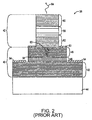
- a VCSEL device 38 includes a short-wavelength VCSEL 40 and a long-wavelength VCSEL 42 that are formed on a single GaAs substrate 44.
- the short-wavelength VCSEL 40 is comprised of an active region 46 and mirrors 48 and 50.
- the mirrors 48 and 50 are made of alternating layers of GaAs and AlGaAs.
- the short-wavelength VCSEL 40 includes metal contacts 52 and 54 that provide current to the activation layer 46.
- the short-wavelength VCSEL 40 includes a current confining scheme which may be realized by proton implantation or by an oxidation layer 56.
- the long-wavelength VCSEL 42 is comprised of an active region 58 and mirrors 60 and 62.
- the mirror 62 is made of alternating layers of GaAs and AlGaAs.
- the mirror 60 can be made of a number of different materials suitable for fabricating a mirror in a VCSEL.
- the mirror 62 is described as being grown in the same epitaxial growth step as the short-wavelength VCSEL 40.
- the operation of the VCSEL device 38 is virtually identical to the operation of the VCSEL device 10 of Fig. 1.
- current is injected into the active region 46 of the short-wavelength VCSEL 40 via the contacts 52 and 54.
- the injected current drives the active region 46 such that light 63 having a short peak wavelength is emitted from the short-wavelength VCSEL 40.
- the light 63 then propagates through the mirror 62 of the long-wavelength VCSEL 42 and impinges upon the active region 58.
- the light 63 is absorbed by the active region 58, which drives the active region 58 to emit laser light 64 having a long peak wavelength.
- the laser light 64 exits the VCSEL device 38 as output laser light from the mirror 60 of the long-wavelength VCSEL 38.
- the output laser light from the VCSEL device 38 will contain a significant amount of the short-wavelength light 63 emitted from the short VCSEL 40.
- a costly filtering device may be required to filter the short-wavelength light 63 and transmit only the laser light 64.
- An optically pumped vertical-cavity surface-emitting laser (VCSEL) device and a method of fabricating the device utilize two separate substrates that perform a filtering operation to selectively transmit only light having a long peak wavelength that is generated by the device.
- the optically pumped VCSEL device is a self-pumped device that can generate the pump light to drive the device to emit output laser light having a long peak wavelength.
- the output laser light has a peak wavelength between 1300 nm and 1550 nm, which is desirable for applications in the field of optical communications.
- the invention is further defined in Claims 1-10.
- the optically pumped VCSEL device includes two VCSELs that are independently formed on the two separate substrates.
- One of the two VCSELs is a current-driven short-wavelength VCSEL, while the other VCSEL is an optically pumped long-wavelength VCSEL.
- the short-wavelength VCSEL provides the light that is utilized to optically pump the long-wavelength VCSEL.
- the long-wavelength VCSEL is configured to emit light having a peak wavelength between 1250 nm and 1700 nm
- the short-wavelength VCSEL is configured to emit light having a peak wavelength of less than 920 nm, with 850 nm being most preferred.
- the short-wavelength VCSEL includes an active region and two distributed Bragg reflector (DBR) mirrors that are formed on one of the two separate substrates.
- the short-wavelength VCSEL may be a conventional VCSEL that is commercially available.
- the substrate in which the short-wavelength VCSEL is formed can be a GaAs substrate.
- the two DBR mirrors may be semiconductor mirrors comprised of materials that are typically utilized to fabricate a short-wavelength VCSEL. As an example, each of the two semiconductor mirrors may be alternating layers of AlGaAs having a low refractive index and AlGaAs having a high refractive index.
- the active region may include GaAs quantum wells.
- the long-wavelength VCSEL includes an active region and two DBR mirrors that are formed on the other substrate.
- the substrate in which the long-wavelength VCSEL is formed can be an InP substrate.
- One of the two DBR mirrors of the long-wavelength VCSEL may be a semiconductor mirror, while the other mirror may be a dielectric mirror.
- the dielectric DBR mirror may be made of alternating layers of SiO 2 and TiO 2 .
- the semiconductor DBR mirror may be made of alternating layers of InGaArP and InP, or alternating layers of InGaAlAs and AlInP or InP.
- the active region may include InGaAsP or AlInGaAs quantum wells.
- the materials utilized to fabricate the components of the long-wavelength VCSEL are not critical to the invention.
- the long-wavelength VCSEL and the short-wavelength VCSEL are bonded together to form the optically pumped VCSEL device.
- the two VCSELs are attached such that the two substrates are separated by the active regions and mirrors of two VCSELs.
- a transparent optical adhesive material or a metallic bonding material may be utilized to bond the short-wavelength VCSEL onto the long-wavelength VCSEL.
- the type of bonding material utilized to couple the two VCSELs is not critical to the invention.
- the optically pumped VCSEL device can be a top-emitting device or a bottom-emitting device.
- the optically pumped VCSEL device is a top-emitting device having the long-wavelength VCSEL located above the short-wavelength VCSEL.
- the short-wavelength VCSEL is initially activated by applying voltage across the active region of the short-wavelength VCSEL, thereby injecting current into the active region.
- the current injection induces the active region to emit first light having a short peak wavelength.
- the emitted first light propagates in an upward direction and in a downward direction.
- the first light propagating in the downward direction is absorbed by the substrate on which the short-wavelength VCSEL has been formed.
- the first light propagating in the upward direction impinges upon the active region of the long-wavelength VCSEL. Much of the first light is then absorbed by the active region of the long-wavelength VCSEL.
- the absorption of the first light drives (i.e., optically pumps) the active region of the long-wavelength VCSEL to emit second light having a long peak wavelength.
- the second light is emitted in upward and downward directions.
- the second light propagating in the upward direction travels through the substrate on which the long-wavelength VCSEL has been formed and escapes the optically pumped VCSEL device as output laser light.
- a high percentage of any of the first light that propagates through the long-wavelength VCSEL is absorbed by the same substrate that allowed the second light to pass. Therefore, the output laser light does not contain a significant amount of the first light having the short peak wavelength.
- the second light propagating in the downward direction travels through the short-wavelength VCSEL and the substrate on which the short-wavelength VCSEL has been formed, thereby exiting the optically pumped VCSEL device.
- a photodiode may be placed below the substrate on which the short-wavelength VCSEL has been formed to monitor the second light emitted by the long-wavelength VCSEL. Since the first light is mostly absorbed by the short-wavelength substrate, the photodiode will essentially be receiving only the second light having the long peak wavelength.
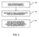
- the method of fabricating an optically pumped VCSEL device in accordance with the present invention includes a step in which a short-wavelength VCSEL is formed on a first substrate.
- a long-wavelength VCSEL is independently formed on a second substrate.
- the short-wavelength VCSEL is then directly bonded onto the long-wavelength VCSEL, such that the first and second substrates are separated by the short-wavelength and long-wavelength VCSELs.
- a transparent optical adhesive material or a metallic bonding material may be utilized to bond the short-wavelength VCSEL onto the long-wavelength VCSEL.
- flip-chip techniques are used for the bonding step.
- the method may include an optional step in which the long-wavelength VCSEL is positioned at an angle with respect to the short-wavelength VCSEL, such that a planar surface of the long-wavelength VCSEL and an opposing planar surface of the short-wavelength VCSEL produce the angle, prior to the bonding step.
- a one-dimensional array or a two-dimensional array of optically pumped VCSEL devices may also be fabricated by bonding an array of long-wavelength VCSELs formed on an InP wafer to an array of short-wavelength VCSELs formed on a GaAs wafer.
- wavelength division multiplexing (WDM) arrays may be fabricated in a similar manner. The fabrication of the WDM array may be accomplished by configuring the array of long-wavelength VCSELs such that each long-wavelength VCSEL on the array of long-wavelength VCSELs is able to generate light having a specified peak wavelength from a selection of wavelengths. The number of different peak wavelengths may vary, depending on the specification of the equipment in which the WDM arrays will be embodied.
- the wavelength variation on the array of long-wavelength VCSELs can be realized by selective-area growth on the InP wafer to develop the long-wavelength VCSELs that can generate light having different peak wavelengths.
- An advantage of the invention is that the two separate sub- . strates absorb almost all of the short-wavelength light emitted by the short-wavelength VCSEL. Therefore, the output laser light is essentially comprised of only the long-wavelength light emitted by the long-wavelength VCSEL. The absorption of the short-wavelength light eliminates the need to place a filtering device to filter the short-wavelength light from the output laser light.
- Another advantage is that since the short-wavelength light does not have to propagate through a substrate to reach the long-wavelength VCSEL, much of the short-wavelength light propagating in a direction toward the long-wavelength VCSEL will reach the long-wavelength VCSEL. Therefore, the light-generating efficiency of the long-wavelength VCSEL is not reduced.
- an optically pumped vertical-cavity surface-emitting laser (VCSEL) device 66 in accordance with the present invention is shown.
- the VCSEL device 66 may be embodied in a telecommunications system (not shown) to transmit optical data.
- the VCSEL device 66 includes a short-wavelength VCSEL 68 formed on a substrate 70 and a long-wavelength VCSEL 72 formed on a substrate 74.
- the substrate 74 is an InP substrate, while the substrate 70 is a semiconductive GaAs substrate, but both substrates may be GaAs without departing from the concept of the invention.
- the short-wavelength VCSEL 68 is designed to emit light 76 having a short peak wavelength in response to current injection.
- the long-wavelength VCSEL 72 is designed to emit light 78 having a long peak wavelength in response to absorption of the short-wavelength light 76. Therefore, the short-wavelength VCSEL 68 drives the long-wavelength VCSEL 72 by emitting the short-wavelength light 76 which optically pumps the long-wavelength VCSEL 72.
- the short-wavelength light 76 has a peak wavelength at 850 nm and the long-wavelength light 78 has a peak wavelength between 1250 nm and 1700 nm.
- the VCSEL device 66 is not a monolithic structure.
- the VCSEL device 66 is made of two separate structures 80 and 82 that have been bonded together.
- the upper structure 80 includes the long-wavelength VCSEL 72 and the substrate 74.
- the lower structure 82 includes contact layers 84 and 86, the short-wavelength VCSEL 68 and the substrate 70.
- the long-wavelength VCSEL 72 and the short-wavelength VCSEL 68 are adjacently positioned such that the substrates 70 and 74 are separated by the VCSELs 68 and 72.
- the two structures 80 and 82 are bonded by an adhesive material 88.
- the adhesive material 88 may be a transparent optical adhesive material or a metallic bonding material.
- the bonding of the structures 80 and 82 is preferably accomplished at a low temperature to ensure that the VCSELs 68 and 72 are not damaged during the bonding process.
- the short-wavelength VCSEL 68 of the structure 82 is comprised of an active region 90 and a current-confining oxidation layer 91 that are sandwiched between mirrors 92 and 94.
- the mirrors 92 and 94 are made of materials typically utilized to fabricate conventional short-wavelength VCSELs.
- the mirrors 92 and 94 are semiconductor distributed Bragg reflectors (DBRs).
- DBRs semiconductor distributed Bragg reflectors
- the mirrors 92 and 94 may be made of alternating layers of a low refractive index AlGaAs and a high refractive index AlGaAs. The difference in refractive indices is caused by a difference in the percentage of Al content in the layers.
- the active region 90 includes GaAs quantum wells (not shown).
- the contact layers 84 and 86 that define the upper and lower surfaces of the structure 82 are made of a metallic material, such as aluminum-germanium-nickel alloy.
- the light-emitting operation of the short-wavelength VCSEL 68 begins when voltage is applied to the contact layers 84 and 86.
- the applied voltage causes current to be injected into the active region 90, causing the quantum wells of the active region 90 to radiate light energy.
- the radiant light energy is reflected between the mirrors 92 and 94. Some of the radiant light energy escapes the cavity defined by the mirrors 92 and 94 as the short-wavelength light 76, which is propagating toward the long-wavelength VCSEL 72. However, some of the radiant light energy escapes the cavity as light having the same wavelength as the light 76 in the direction of the substrate 70. This light is eventually absorbed by the substrate 70.
- the properties of the substrate 70 are such that light having a wavelength of approximately 850 nm or shorter will be absorbed by the substrate.
- the long-wavelength VCSEL 72 of the upper structure 80 is comprised of an active region 96 located between mirrors 98 and 100.
- the mirror 98 is a semiconductor DBR, while the mirror 100 is a dielectric DBR.
- the semiconductor DBR mirror 98 may be made of alternating layers of InGaArP and InP. In an alternative configuration, the mirror 98 may be made of alternating layers of InGaAlAs and InP or AlInP.
- the dielectric DBR mirror 100 may be made of alternating layers of SiO 2 and TiO 2 , but other dielectric materials may be used.
- the active region 96 may include InGaAsP or AllnGaAs quantum wells (not shown). The materials utilized to fabricate the active region 96 and the mirrors 98 and 100 are not critical to the invention.
- the long-wavelength VCSEL 72 operates to generate the long-wavelength light 78 by absorbing the short-wavelength light 76 emitted from the short-wavelength VCSEL 68.
- the emitted short-wavelength light 76 propagates through the bottom mirror 100 of the long-wavelength VCSEL 72 and is absorbed by the active region 96.
- the absorption of the short-wavelength light 76 by the active region 96 drives the active region 96 to emit long-wavelength light.
- Some of the emitted long-wavelength light propagates in an upward direction toward the substrate 74. However, some of the long-wavelength light is emitted by the active region 96 in a downward direction toward the short-wavelength VCSEL 68.
- This long-wavelength light propagates through the short-wavelength VCSEL 68 and the GaAs substrate 70.
- the downward propagating long-wavelength light eventually escapes the VCSEL device 66, exiting from the contact layer 86. Since the short-wavelength light emitted from the short-wavelength VCSEL 68 is absorbed by the substrate 70, the only light exiting the VCSEL 66 from the contact layer 86 is a portion of the long-wavelength light emitted from the long-wavelength VCSEL 72. Therefore, the intensity of the long-wavelength light generated by the long-wavelength VCSEL 72 may be monitored by placing a photodiode below the contact layer 86.
- the long-wavelength light that is emitted in the upward direction toward the substrate 74 propagates through the mirror 98 and the substrate 74.
- the substrate 74 is configured to absorb light having a wavelength of approximately 920 nm or shorter.
- the short-wavelength light 76 emitted from the short-wavelength VCSEL 68 has a peak wavelength of 850 nm
- the long-wavelength light emitted from the long-wavelength VCSEL 72 has a peak wavelength between 1250 nm-1700 nm. Therefore, the short-wavelength light 76 will be absorbed by the substrate 74 and only the long-wavelength light 78 will be able to propagate through the substrate 74.
- the substrate 74 in effect, filters short-wavelength light 76 that propagates through the substrate 74, eliminating the need to have an external filter placed between the substrate 74 and an associated fiber optic cable (not shown).
- the upper structure 80 is tilted with respect to the planar surface of the lower structure 82. This may be achieved by increasing the thickness of the adhesive material 88 on one side of the upper structure 80. The tilting of the upper structure 80 creates an angle between the facing planar surfaces of the short-wavelength VCSEL 68 and the long-wavelength VCSEL 72. The angle prevents much of the short-wavelength light 76 that is reflected by the lower surface of the long-wavelength VCSEL 72 from being transmitted back into the short-wavelength VCSEL 68.
- a short-wavelength VCSEL is formed on a first substrate.
- the short-wavelength VCSEL may be a conventional current-driven VCSEL.
- the short-wavelength VCSEL is configured to emit light having a peak wavelength of 850 nm.
- a long-wavelength VCSEL is independently formed on a second substrate.
- the long-wavelength VCSEL is configured to emit light having a peak wavelength between 1300 nm and 1550 nm, by absorbing the short-wavelength light emitted from the short-wavelength VCSEL.
- the first and second substrates have a common transmittance characteristic of absorbing the light emitted from the short-wavelength VCSEL, while allowing the light emitted from the long-wavelength VCSEL to be transmitted through the substrates.
- the short-wavelength VCSEL is directly bonded onto the long-wavelength VCSEL, such that the first and second substrates are separated by the short-wavelength and long-wavelength VCSELs.
- a transparent optical adhesive material or a metallic bonding material may be utilized to bond the short-wavelength VCSEL onto the long-wavelength VCSEL.
- flip-chip techniques are used for the bonding step.
- the method may include an optional step of positioning the long-wavelength VCSEL at an angle with respect to the short-wavelength VCSEL, such that a planar surface of the long-wavelength VCSEL and an opposing planar surface of the short-wavelength VCSEL produce the angle, prior to the step 106.
- a one-dimensional array or a two-dimensional array of optically pumped VCSEL devices may be fabricated by bonding an array of long-wavelength VCSELs formed on an InP wafer to an array of short-wavelength VCSELs formed on a GaAs wafer.
- a wavelength division multiplexing (WDM) array may be fabricated in a similar manner. The fabrication of the WDM array may be accomplished by configuring the array of long-wavelength VCSELs such that each long-wavelength VCSEL on the array of long-wavelength VCSELs is able to generate light having a specified peak wavelength from a selection of wavelengths.
- the number of different peak wavelengths may vary depending on the specification of the equipment in which the WDM arrays will be embodied.
- the wavelength variation on the array of long-wavelength VCSELs can be realized by selective-area growth on the InP wafer to develop the long-wavelength VCSELs that can generate light having different peak wavelengths.
Landscapes
- Physics & Mathematics (AREA)
- Condensed Matter Physics & Semiconductors (AREA)
- General Physics & Mathematics (AREA)
- Electromagnetism (AREA)
- Optics & Photonics (AREA)
- Semiconductor Lasers (AREA)
Applications Claiming Priority (2)
| Application Number | Priority Date | Filing Date | Title |
|---|---|---|---|
| US09/263,696 US6252896B1 (en) | 1999-03-05 | 1999-03-05 | Long-Wavelength VCSEL using buried bragg reflectors |
| US263696 | 1999-03-05 |
Publications (3)
| Publication Number | Publication Date |
|---|---|
| EP1037341A2 EP1037341A2 (en) | 2000-09-20 |
| EP1037341A3 EP1037341A3 (en) | 2001-09-05 |
| EP1037341B1 true EP1037341B1 (en) | 2003-05-02 |
Family
ID=23002879
Family Applications (1)
| Application Number | Title | Priority Date | Filing Date |
|---|---|---|---|
| EP00102463A Expired - Lifetime EP1037341B1 (en) | 1999-03-05 | 2000-02-04 | Optically pumped VCSEL |
Country Status (4)
| Country | Link |
|---|---|
| US (1) | US6252896B1 (ja) |
| EP (1) | EP1037341B1 (ja) |
| JP (1) | JP2000261096A (ja) |
| DE (1) | DE60002387T2 (ja) |
Families Citing this family (52)
| Publication number | Priority date | Publication date | Assignee | Title |
|---|---|---|---|---|
| US7257143B2 (en) * | 1998-12-21 | 2007-08-14 | Finisar Corporation | Multicomponent barrier layers in quantum well active regions to enhance confinement and speed |
| US20030219917A1 (en) * | 1998-12-21 | 2003-11-27 | Johnson Ralph H. | System and method using migration enhanced epitaxy for flattening active layers and the mechanical stabilization of quantum wells associated with vertical cavity surface emitting lasers |
| US7435660B2 (en) * | 1998-12-21 | 2008-10-14 | Finisar Corporation | Migration enhanced epitaxy fabrication of active regions having quantum wells |
| US7095770B2 (en) | 2001-12-20 | 2006-08-22 | Finisar Corporation | Vertical cavity surface emitting laser including indium, antimony and nitrogen in the active region |
| US6922426B2 (en) | 2001-12-20 | 2005-07-26 | Finisar Corporation | Vertical cavity surface emitting laser including indium in the active region |
| US7167495B2 (en) * | 1998-12-21 | 2007-01-23 | Finisar Corporation | Use of GaAs extended barrier layers between active regions containing nitrogen and AlGaAs confining layers |
| US7058112B2 (en) | 2001-12-27 | 2006-06-06 | Finisar Corporation | Indium free vertical cavity surface emitting laser |
| US7286585B2 (en) * | 1998-12-21 | 2007-10-23 | Finisar Corporation | Low temperature grown layers with migration enhanced epitaxy adjacent to an InGaAsN(Sb) based active region |
| US6975660B2 (en) | 2001-12-27 | 2005-12-13 | Finisar Corporation | Vertical cavity surface emitting laser including indium and antimony in the active region |
| US7408964B2 (en) | 2001-12-20 | 2008-08-05 | Finisar Corporation | Vertical cavity surface emitting laser including indium and nitrogen in the active region |
| US6445495B1 (en) * | 1999-03-22 | 2002-09-03 | Genoa Corporation | Tunable-gain lasing semiconductor optical amplifier |
| US6891664B2 (en) | 1999-03-22 | 2005-05-10 | Finisar Corporation | Multistage tunable gain optical amplifier |
| WO2001031756A1 (en) * | 1999-10-29 | 2001-05-03 | E20 Communications, Inc. | Modulated integrated optically pumped vertical cavity surface emitting lasers |
| US6424669B1 (en) | 1999-10-29 | 2002-07-23 | E20 Communications, Inc. | Integrated optically pumped vertical cavity surface emitting laser |
| US6879615B2 (en) * | 2000-01-19 | 2005-04-12 | Joseph Reid Henrichs | FCSEL that frequency doubles its output emissions using sum-frequency generation |
| US6936900B1 (en) * | 2000-05-04 | 2005-08-30 | Osemi, Inc. | Integrated transistor devices |
| US6573528B2 (en) * | 2000-10-12 | 2003-06-03 | Walter David Braddock | Detector diode with internal calibration structure |
| US6434180B1 (en) * | 2000-12-19 | 2002-08-13 | Lucent Technologies Inc. | Vertical cavity surface emitting laser (VCSEL) |
| US6556610B1 (en) | 2001-04-12 | 2003-04-29 | E20 Communications, Inc. | Semiconductor lasers |
| WO2003001636A1 (de) | 2001-06-20 | 2003-01-03 | Infineon Technologies Ag | Photonen-emitter und datenübertragungsvorrichtung |
| DE10134825A1 (de) * | 2001-06-20 | 2003-01-09 | Infineon Technologies Ag | Photonen-Emitter und Datenübertragungsvorrichtung |
| US6717964B2 (en) | 2001-07-02 | 2004-04-06 | E20 Communications, Inc. | Method and apparatus for wavelength tuning of optically pumped vertical cavity surface emitting lasers |
| US6647050B2 (en) * | 2001-09-18 | 2003-11-11 | Agilent Technologies, Inc. | Flip-chip assembly for optically-pumped lasers |
| FR2833758B1 (fr) * | 2001-12-13 | 2004-12-10 | Commissariat Energie Atomique | Dispositif d'emission de lumiere a micro-cavite et procede de fabrication de ce dispositif |
| US6891865B1 (en) * | 2002-02-15 | 2005-05-10 | Afonics Fibreoptics, Ltd. | Wavelength tunable laser |
| US7295586B2 (en) * | 2002-02-21 | 2007-11-13 | Finisar Corporation | Carbon doped GaAsSb suitable for use in tunnel junctions of long-wavelength VCSELs |
| US6822995B2 (en) * | 2002-02-21 | 2004-11-23 | Finisar Corporation | GaAs/AI(Ga)As distributed bragg reflector on InP |
| US6989556B2 (en) * | 2002-06-06 | 2006-01-24 | Osemi, Inc. | Metal oxide compound semiconductor integrated transistor devices with a gate insulator structure |
| US7187045B2 (en) * | 2002-07-16 | 2007-03-06 | Osemi, Inc. | Junction field effect metal oxide compound semiconductor integrated transistor devices |
| JP2004207480A (ja) * | 2002-12-25 | 2004-07-22 | Pioneer Electronic Corp | 半導体レーザ装置及びその製造方法 |
| KR101180166B1 (ko) * | 2003-11-13 | 2012-09-05 | 오스람 옵토 세미컨덕터스 게엠베하 | 반도체 레이저 장치 |
| WO2005048318A2 (en) * | 2003-11-17 | 2005-05-26 | Osemi, Inc. | Nitride metal oxide semiconductor integrated transistor devices |
| WO2005061756A1 (en) * | 2003-12-09 | 2005-07-07 | Osemi, Inc. | High temperature vacuum evaporation apparatus |
| US6947466B2 (en) * | 2004-01-29 | 2005-09-20 | Coherent, Inc. | Optically pumped edge-emitting semiconductor laser |
| DE102004004781A1 (de) * | 2004-01-30 | 2005-08-18 | Osram Opto Semiconductors Gmbh | Strahlungsemittierendes Halbleiterbauelement |
| FR2867900A1 (fr) * | 2004-03-16 | 2005-09-23 | Commissariat Energie Atomique | Dispositif d'emission de lumiere avec une structure emettrice a micro-cavite et une diode de pompe a cavite verticale et procede de fabrication |
| JP4602685B2 (ja) * | 2004-04-14 | 2010-12-22 | 株式会社リコー | 垂直共振器型面発光半導体レーザ素子および発光装置および光伝送システム |
| FR2870051B1 (fr) * | 2004-05-04 | 2009-04-03 | Commissariat Energie Atomique | Emetteur de rayonnement avec faisceau de pompage incline |
| US7372886B2 (en) | 2004-06-07 | 2008-05-13 | Avago Technologies Fiber Ip Pte Ltd | High thermal conductivity vertical cavity surface emitting laser (VCSEL) |
| CN101432936B (zh) | 2004-10-01 | 2011-02-02 | 菲尼萨公司 | 具有多顶侧接触的垂直腔面发射激光器 |
| US7860137B2 (en) | 2004-10-01 | 2010-12-28 | Finisar Corporation | Vertical cavity surface emitting laser with undoped top mirror |
| US7719015B2 (en) * | 2004-12-09 | 2010-05-18 | 3M Innovative Properties Company | Type II broadband or polychromatic LED's |
| US7745814B2 (en) * | 2004-12-09 | 2010-06-29 | 3M Innovative Properties Company | Polychromatic LED's and related semiconductor devices |
| US7402831B2 (en) * | 2004-12-09 | 2008-07-22 | 3M Innovative Properties Company | Adapting short-wavelength LED's for polychromatic, broadband, or “white” emission |
| US7453629B2 (en) * | 2005-12-29 | 2008-11-18 | Lucent Technologies Inc. | Semiconductor optical amplifier pulse reshaper |
| JP5214140B2 (ja) * | 2006-12-12 | 2013-06-19 | 浜松ホトニクス株式会社 | 半導体発光素子 |
| US7433374B2 (en) * | 2006-12-21 | 2008-10-07 | Coherent, Inc. | Frequency-doubled edge-emitting semiconductor lasers |
| WO2009075972A2 (en) * | 2007-12-10 | 2009-06-18 | 3M Innovative Properties Company | Down-converted light emitting diode with simplified light extraction |
| DE102008048903B4 (de) * | 2008-09-25 | 2021-06-24 | OSRAM Opto Semiconductors Gesellschaft mit beschränkter Haftung | Optoelektronisches Bauteil |
| SE534345C2 (sv) * | 2009-09-24 | 2011-07-19 | Svedice Ab | Fotodiod av typen lavinfotodiod. |
| DE102014200583B3 (de) * | 2014-01-15 | 2015-05-13 | Robert Bosch Gmbh | Verfahren zum herstellen eines integrierten mikromechanischen fluidsensor-bauteils, integriertes mikromechanisches fluidsensor-bauteil und verfahren zum detektieren eines fluids mittels eines integrierten mikromechanischen fluidsensor-bauteils |
| CN111740312B (zh) * | 2020-06-28 | 2023-04-07 | 海南师范大学 | 一种双波长单片集成面发射半导体激光器 |
Family Cites Families (6)
| Publication number | Priority date | Publication date | Assignee | Title |
|---|---|---|---|---|
| JP2576692B2 (ja) * | 1993-07-14 | 1997-01-29 | 日本電気株式会社 | 波長多重用光デバイスの製造方法 |
| US5363390A (en) * | 1993-11-22 | 1994-11-08 | Hewlett-Packard Company | Semiconductor laser that generates second harmonic light by means of a nonlinear crystal in the laser cavity |
| US5513204A (en) | 1995-04-12 | 1996-04-30 | Optical Concepts, Inc. | Long wavelength, vertical cavity surface emitting laser with vertically integrated optical pump |
| DE19523267A1 (de) * | 1995-06-27 | 1997-01-02 | Bosch Gmbh Robert | Lasermodul |
| US5754578A (en) | 1996-06-24 | 1998-05-19 | W. L. Gore & Associates, Inc. | 1250-1650 nm vertical cavity surface emitting laser pumped by a 700-1050 nm vertical cavity surface emitting laser |
| FR2751796B1 (fr) * | 1996-07-26 | 1998-08-28 | Commissariat Energie Atomique | Microlaser soilde, a pompage optique par laser semi-conducteur a cavite verticale |
-
1999
- 1999-03-05 US US09/263,696 patent/US6252896B1/en not_active Expired - Lifetime
-
2000
- 2000-02-04 DE DE60002387T patent/DE60002387T2/de not_active Expired - Fee Related
- 2000-02-04 EP EP00102463A patent/EP1037341B1/en not_active Expired - Lifetime
- 2000-03-01 JP JP2000055745A patent/JP2000261096A/ja not_active Withdrawn
Also Published As
| Publication number | Publication date |
|---|---|
| DE60002387D1 (de) | 2003-06-05 |
| EP1037341A3 (en) | 2001-09-05 |
| US6252896B1 (en) | 2001-06-26 |
| DE60002387T2 (de) | 2004-02-12 |
| EP1037341A2 (en) | 2000-09-20 |
| JP2000261096A (ja) | 2000-09-22 |
Similar Documents
| Publication | Publication Date | Title |
|---|---|---|
| EP1037341B1 (en) | Optically pumped VCSEL | |
| KR100229051B1 (ko) | 수직적으로 통합된 광학펌프를 갖는 장파장수직 공동표면 방출레이저 | |
| US6055262A (en) | Resonant reflector for improved optoelectronic device performance and enhanced applicability | |
| US6940885B1 (en) | Systems, methods, and apparatuses for optically pumped vertical cavity surface emitting laser devices | |
| US6088376A (en) | Vertical-cavity-surface-emitting semiconductor devices with fiber-coupled optical cavity | |
| US5754578A (en) | 1250-1650 nm vertical cavity surface emitting laser pumped by a 700-1050 nm vertical cavity surface emitting laser | |
| US7288421B2 (en) | Method for forming an optoelectronic device having an isolation layer | |
| EP0892474B1 (en) | Field modulated vertical cavity surface-emitting laser with internal optical pumping | |
| WO2011090573A2 (en) | Hybrid silicon vertical cavity laser with in-plane coupling | |
| CA2328637A1 (en) | Lateral optical pumping of vertical cavity surface emitting laser | |
| US5918108A (en) | Vertical cavity surface emitting laser with enhanced second harmonic generation and method of making same | |
| WO2012005012A2 (en) | Optical interconnection system | |
| US6553051B1 (en) | System for optically pumping a long wavelength laser using a short wavelength laser | |
| US5422898A (en) | Tapered Fabry-Perot multi-wavelength optical source | |
| Syrbu et al. | 1.55-μm optically pumped wafer-fused tunable VCSELs with 32-nm tuning range | |
| JP2002252418A (ja) | 光通信システム | |
| Jayaraman et al. | WDM array using long-wavelength vertical-cavity lasers | |
| WO2000062384A1 (en) | Intra-cavity optically pumped vertical cavity surface emitting laser | |
| KR20030045252A (ko) | 장파장 면발광 반도체 레이저 다이오드 | |
| KR100212460B1 (ko) | 장파장 표면방출 레이저 칩 및 그 제조방법 | |
| WO2002075879A1 (en) | Vertical-cavity surface-emitting laser (vcsel) with cavity compensated gain | |
| US20020176470A1 (en) | Phase compensated distributed bragg reflector | |
| JPH11195833A (ja) | 発光デバイスおよびその使用方法 |
Legal Events
| Date | Code | Title | Description |
|---|---|---|---|
| PUAI | Public reference made under article 153(3) epc to a published international application that has entered the european phase |
Free format text: ORIGINAL CODE: 0009012 |
|
| AK | Designated contracting states |
Kind code of ref document: A2 Designated state(s): AT BE CH CY DE DK ES FI FR GB GR IE IT LI LU MC NL PT SE |
|
| AX | Request for extension of the european patent |
Free format text: AL;LT;LV;MK;RO;SI |
|
| PUAL | Search report despatched |
Free format text: ORIGINAL CODE: 0009013 |
|
| RAP1 | Party data changed (applicant data changed or rights of an application transferred) |
Owner name: AGILENT TECHNOLOGIES INC. |
|
| RAP1 | Party data changed (applicant data changed or rights of an application transferred) |
Owner name: AGILENT TECHNOLOGIES INC. A DELAWARE CORPORATION |
|
| AK | Designated contracting states |
Kind code of ref document: A3 Designated state(s): AT BE CH CY DE DK ES FI FR GB GR IE IT LI LU MC NL PT SE |
|
| AX | Request for extension of the european patent |
Free format text: AL;LT;LV;MK;RO;SI |
|
| RAP1 | Party data changed (applicant data changed or rights of an application transferred) |
Owner name: AGILENT TECHNOLOGIES, INC. (A DELAWARE CORPORATION |
|
| 17P | Request for examination filed |
Effective date: 20011114 |
|
| 17Q | First examination report despatched |
Effective date: 20020122 |
|
| AKX | Designation fees paid |
Free format text: DE FR GB |
|
| GRAH | Despatch of communication of intention to grant a patent |
Free format text: ORIGINAL CODE: EPIDOS IGRA |
|
| GRAH | Despatch of communication of intention to grant a patent |
Free format text: ORIGINAL CODE: EPIDOS IGRA |
|
| GRAA | (expected) grant |
Free format text: ORIGINAL CODE: 0009210 |
|
| AK | Designated contracting states |
Designated state(s): DE FR GB |
|
| REG | Reference to a national code |
Ref country code: GB Ref legal event code: FG4D |
|
| REF | Corresponds to: |
Ref document number: 60002387 Country of ref document: DE Date of ref document: 20030605 Kind code of ref document: P |
|
| ET | Fr: translation filed | ||
| PLBE | No opposition filed within time limit |
Free format text: ORIGINAL CODE: 0009261 |
|
| STAA | Information on the status of an ep patent application or granted ep patent |
Free format text: STATUS: NO OPPOSITION FILED WITHIN TIME LIMIT |
|
| 26N | No opposition filed |
Effective date: 20040203 |
|
| PGFP | Annual fee paid to national office [announced via postgrant information from national office to epo] |
Ref country code: FR Payment date: 20060217 Year of fee payment: 7 |
|
| REG | Reference to a national code |
Ref country code: GB Ref legal event code: 732E |
|
| PGFP | Annual fee paid to national office [announced via postgrant information from national office to epo] |
Ref country code: DE Payment date: 20070330 Year of fee payment: 8 |
|
| REG | Reference to a national code |
Ref country code: FR Ref legal event code: ST Effective date: 20071030 |
|
| PG25 | Lapsed in a contracting state [announced via postgrant information from national office to epo] |
Ref country code: FR Free format text: LAPSE BECAUSE OF NON-PAYMENT OF DUE FEES Effective date: 20070228 |
|
| PG25 | Lapsed in a contracting state [announced via postgrant information from national office to epo] |
Ref country code: DE Free format text: LAPSE BECAUSE OF NON-PAYMENT OF DUE FEES Effective date: 20080902 |
|
| PGFP | Annual fee paid to national office [announced via postgrant information from national office to epo] |
Ref country code: GB Payment date: 20130130 Year of fee payment: 14 |
|
| GBPC | Gb: european patent ceased through non-payment of renewal fee |
Effective date: 20140204 |
|
| PG25 | Lapsed in a contracting state [announced via postgrant information from national office to epo] |
Ref country code: GB Free format text: LAPSE BECAUSE OF NON-PAYMENT OF DUE FEES Effective date: 20140204 |