EP1036364B1 - Alignment of cluster address to block addresses within a semiconductor non-volatile mass storage memory - Google Patents
Alignment of cluster address to block addresses within a semiconductor non-volatile mass storage memory Download PDFInfo
- Publication number
- EP1036364B1 EP1036364B1 EP98959628A EP98959628A EP1036364B1 EP 1036364 B1 EP1036364 B1 EP 1036364B1 EP 98959628 A EP98959628 A EP 98959628A EP 98959628 A EP98959628 A EP 98959628A EP 1036364 B1 EP1036364 B1 EP 1036364B1
- Authority
- EP
- European Patent Office
- Prior art keywords
- block
- lba
- address
- memory unit
- nonvolatile memory
- Prior art date
- Legal status (The legal status is an assumption and is not a legal conclusion. Google has not performed a legal analysis and makes no representation as to the accuracy of the status listed.)
- Expired - Lifetime
Links
Images



Classifications
-
- G—PHYSICS
- G06—COMPUTING OR CALCULATING; COUNTING
- G06F—ELECTRIC DIGITAL DATA PROCESSING
- G06F12/00—Accessing, addressing or allocating within memory systems or architectures
- G06F12/02—Addressing or allocation; Relocation
- G06F12/0223—User address space allocation, e.g. contiguous or non contiguous base addressing
- G06F12/023—Free address space management
-
- G—PHYSICS
- G06—COMPUTING OR CALCULATING; COUNTING
- G06F—ELECTRIC DIGITAL DATA PROCESSING
- G06F12/00—Accessing, addressing or allocating within memory systems or architectures
- G06F12/02—Addressing or allocation; Relocation
- G06F12/0223—User address space allocation, e.g. contiguous or non contiguous base addressing
- G06F12/023—Free address space management
- G06F12/0238—Memory management in non-volatile memory, e.g. resistive RAM or ferroelectric memory
- G06F12/0246—Memory management in non-volatile memory, e.g. resistive RAM or ferroelectric memory in block erasable memory, e.g. flash memory
-
- G—PHYSICS
- G06—COMPUTING OR CALCULATING; COUNTING
- G06F—ELECTRIC DIGITAL DATA PROCESSING
- G06F3/00—Input arrangements for transferring data to be processed into a form capable of being handled by the computer; Output arrangements for transferring data from processing unit to output unit, e.g. interface arrangements
- G06F3/06—Digital input from, or digital output to, record carriers, e.g. RAID, emulated record carriers or networked record carriers
- G06F3/0601—Interfaces specially adapted for storage systems
- G06F3/0602—Interfaces specially adapted for storage systems specifically adapted to achieve a particular effect
- G06F3/061—Improving I/O performance
-
- G—PHYSICS
- G06—COMPUTING OR CALCULATING; COUNTING
- G06F—ELECTRIC DIGITAL DATA PROCESSING
- G06F3/00—Input arrangements for transferring data to be processed into a form capable of being handled by the computer; Output arrangements for transferring data from processing unit to output unit, e.g. interface arrangements
- G06F3/06—Digital input from, or digital output to, record carriers, e.g. RAID, emulated record carriers or networked record carriers
- G06F3/0601—Interfaces specially adapted for storage systems
- G06F3/0628—Interfaces specially adapted for storage systems making use of a particular technique
- G06F3/0638—Organizing or formatting or addressing of data
- G06F3/064—Management of blocks
-
- G—PHYSICS
- G06—COMPUTING OR CALCULATING; COUNTING
- G06F—ELECTRIC DIGITAL DATA PROCESSING
- G06F3/00—Input arrangements for transferring data to be processed into a form capable of being handled by the computer; Output arrangements for transferring data from processing unit to output unit, e.g. interface arrangements
- G06F3/06—Digital input from, or digital output to, record carriers, e.g. RAID, emulated record carriers or networked record carriers
- G06F3/0601—Interfaces specially adapted for storage systems
- G06F3/0668—Interfaces specially adapted for storage systems adopting a particular infrastructure
- G06F3/0671—In-line storage system
- G06F3/0673—Single storage device
- G06F3/0679—Non-volatile semiconductor memory device, e.g. flash memory, one time programmable memory [OTP]
-
- G—PHYSICS
- G11—INFORMATION STORAGE
- G11C—STATIC STORES
- G11C16/00—Erasable programmable read-only memories
- G11C16/02—Erasable programmable read-only memories electrically programmable
- G11C16/06—Auxiliary circuits, e.g. for writing into memory
- G11C16/08—Address circuits; Decoders; Word-line control circuits
-
- G—PHYSICS
- G11—INFORMATION STORAGE
- G11C—STATIC STORES
- G11C16/00—Erasable programmable read-only memories
- G11C16/02—Erasable programmable read-only memories electrically programmable
- G11C16/06—Auxiliary circuits, e.g. for writing into memory
- G11C16/10—Programming or data input circuits
- G11C16/102—External programming circuits, e.g. EPROM programmers; In-circuit programming or reprogramming; EPROM emulators
-
- G—PHYSICS
- G11—INFORMATION STORAGE
- G11C—STATIC STORES
- G11C29/00—Checking stores for correct operation ; Subsequent repair; Testing stores during standby or offline operation
- G11C29/70—Masking faults in memories by using spares or by reconfiguring
- G11C29/76—Masking faults in memories by using spares or by reconfiguring using address translation or modifications
- G11C29/765—Masking faults in memories by using spares or by reconfiguring using address translation or modifications in solid state disks
-
- G—PHYSICS
- G11—INFORMATION STORAGE
- G11C—STATIC STORES
- G11C29/00—Checking stores for correct operation ; Subsequent repair; Testing stores during standby or offline operation
- G11C29/70—Masking faults in memories by using spares or by reconfiguring
- G11C29/78—Masking faults in memories by using spares or by reconfiguring using programmable devices
- G11C29/80—Masking faults in memories by using spares or by reconfiguring using programmable devices with improved layout
- G11C29/816—Masking faults in memories by using spares or by reconfiguring using programmable devices with improved layout for an application-specific layout
- G11C29/82—Masking faults in memories by using spares or by reconfiguring using programmable devices with improved layout for an application-specific layout for EEPROMs
-
- G—PHYSICS
- G06—COMPUTING OR CALCULATING; COUNTING
- G06F—ELECTRIC DIGITAL DATA PROCESSING
- G06F11/00—Error detection; Error correction; Monitoring
- G06F11/07—Responding to the occurrence of a fault, e.g. fault tolerance
- G06F11/08—Error detection or correction by redundancy in data representation, e.g. by using checking codes
- G06F11/10—Adding special bits or symbols to the coded information, e.g. parity check, casting out 9's or 11's
- G06F11/1008—Adding special bits or symbols to the coded information, e.g. parity check, casting out 9's or 11's in individual solid state devices
- G06F11/1068—Adding special bits or symbols to the coded information, e.g. parity check, casting out 9's or 11's in individual solid state devices in sector programmable memories, e.g. flash disk
Definitions
- This invention relates generally to semiconductor mass storage systems and methods of operating thereof, and more particularly to digital systems, such as PCs, using nonvolatile memory devices in lieu of conventional hard disk drives and digital cameras using nonvolatile memory devices in lieu of conventional films for storage of large quantities of informational data wherein the information being stored in the nonvolatile memory is organized and aligned in such a way so as to maximize the performance of the digital system.
- Solid state memory is an ideal choice for replacing a hard disk drive for mass storage because it can resolve the problems cited above.
- Potential solutions have been proposed for replacing a hard disk drive with a semiconductor memory.
- the memory must be non-volatile and alterable.
- the inventors have determined that FLASH memory is preferred for such a replacement.
- solid state memory is employed to maintain the digital information that is collected, such as a picture frame, to replace the films used in conventional cameras.
- the digital system which may appear in the form of a card, is inserted in a computer where it may be edited, stored or used in other ways.
- the memory that is used to maintain the picture frames must also be nonvolatile yet alterable; FLASH memory is a viable device for such usage.
- Devices manufactured using technologies such as FLASH memory need to be programmed before erasing to improve uniformity amongst all cells. They also have to be verified for successful erase.
- One requirement for successfully employing a semiconductor mass storage device in lieu of rotating media hard disk mass storage device or film is that its use must be transparent to the computer's operating system and the user of a system using such a device. In other words, the designer or user of a computer incorporating such a semiconductor mass storage device could simply remove the hard disk and replace it with a semiconductor mass storage device. All presently available commercial software should operate on a system employing such a semiconductor mass storage device without the necessity of any modification.
- Conventional computer systems include a mass storage memory facility for storing user information such as data and applications files (user files).
- user files data and applications files
- conventional systems also store non-user information in the mass storage memory facility for use by the computer system in controlling the general operation of the computer and its related peripheral systems (system files).
- system information includes the boot sector, the FAT tables and the directory information.
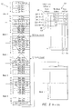
- Fig. 1 is an example of the organization of user data information in nonvolatile memory unit 100 and a look-up-table 102 preferably stored within a volatile memory unit (not shown) as employed by a prior art system.
- Look-up-table 102 represents a mapping of LBAs to corresponding block addresses within the nonvolatile memory unit 102 wherein the user data file is actually stored.
- Each LBA identifies the location of a 512 byte (or a sector) portion of the user data file.
- a block within the nonvolatile memory unit 100 comprises of 16 LBAs and therefore each row of the look-up-table 102 (such as 104, 106, 108, ...) includes information regarding the status of a 16-sector block.
- the block address field 110 in look-up-table 102 specifies the block location within the nonvolatile memory where information identified by LBA values resides.
- information identified by LBAs 0-15 correspond to block address 0.
- a ⁇ used' flag field 112 and an 'old' flag field 114 identify the state of a block within the nonvolatile memory.
- the 'used' flag field 112 when set to a logic state 1' indicates that the block identified by the corresponding block address 110 of the row in which the 'used' flag resides has been written to and is therefore in use, whereas a logic state '0'. as represented by the 'used' flag, indicates that the block is available or free to be written.
- a logic state of '1' represented by the ⁇ old' flag 114 indicates that the block addressed by the block address of the corresponding row in which the used flag resides is not to be accessed prior to being erased.
- the nonvolatile memory 100 wherein the user files are stored is organized into blocks, such as Block 0, Block 1, etc.
- Each such block within the nonvolatile memory is identified by an address represented by the block address field 110 and comprises of 16 sectors.
- Block 0, Block I and Block 2 were previously written, as indicated by the state of their corresponding 'used' flags in look-up-table 102.
- Fig. 2 the example cited above is carried through to illustrate the case where 8 sectors starting from LBA 29 (or 'ID' in Hexadecimal notation) is updated with new information.
- LBA 29 or 'ID' in Hexadecimal notation
- Block 1 the location in nonvolatile memory 100 wherein LBA 29, for example, was stored, i.e., Block 1, can not be re-written because no erase operations were performed since the last write operation to this location.
- the information that is to be updated in LBA 29 through 37 then needs to be stored elsewhere, in an available location within the nonvolatile memory 100.
- Block 3 the information identified by LBA 29, 30, and 31 is written to Block 3 of the nonvolatile memory 100 and even though the information identified by LBA 16-28 is not being effected, it is nevertheless moved from Block I to Block 3 of the nonvolatile memory 100. This is due to setting the state of Block 1 to where it can be erased. In other words, the information that resided in Block 1 that was not to be accessed is still having to be moved in order to allow erasure of that block. In fact, this is the reason for setting the state of the 'old' flag 114 of row 106 in the look-up-table 102 to logic state ⁇ 1'.
- LBA 32-36 The remainder of the LBA-identified information, i.e. LBA 32-36, is written to the next available block within nonvolatile memory 100, such as Block 4. Information identified by LBA 32-36 is written to sectors 0-4, respectively, of Block 4. Furthermore, since LBA 32-47 in row 108 corresponded to Block 2 previously (see Fig. 1 ), sectors 5-15 of Block 2 are then moved to like sector locations of Block 4, after which Block 2 may be erased.
- a method and apparatus is therefore needed for updating user files, having various block sizes, that are maintained in nonvolatile memory devices of digital systems, such as PCs and digital cameras, whereby the number of move and therefore write operations is minimized resulting in increased system performance.
- US-A-5337275 describes a flash memory system where, once any one of the blocks of a memory array has been erased, data may be written to any position on the entire block.
- a host begins writing data to be stored in the array to a block of the array having free space
- the data to be stored in the array is written sequentially, sector by sector, to the free space in this block until the block has been filled with the data. Then, writing proceeds to the next sequential block having free space.
- a preferred embodiment of the present invention includes a digital system for use with a host, the digital system including a nonvolatile memory unit having memory locations organized in blocks with each block having a plurality of sectors for storing information provided by the host, through a controller, in the form of non-user data files and user data files.
- the controller being operative to control the reading, writing and erasing operations performed on the nonvolatile memory, the host for providing an address identifying the starting location of the user file to the controller wherein the host provides a user file identified by a starting sector address for storage within the nonvolatile memory unit to the controller.
- the controller finds a free block within the nonvolatile memory unit that is available for storage of information and aligns the user file starting address with the beginning of the free block and stores the user file within the free block starting with the beginning of the free block. If the user file extends beyond the size of the free block, storing the remainder of the user file within blocks subsequent to the free block, wherein each time a user data file is stored in the nonvolatile memory unit, the beginning of the user data file is aligned with the beginning of the block thereby increasing the performance of writing user files and decreasing the number of erase and write operations performed on the nonvolatile memory unit.
- a general high-level block diagram of a digital system 500 such as a digital camera or a personal computer (PC) is depicted to include a controller 506 for performing operations, such as writing, reading and erasing, on a non-volatile memory unit 508.
- the controller 506 is coupled to a host 502, which may be a central processing unit (CPU), commonly employed in digital systems, that initiates reading and writing operations to be performed on the nonvolatile memory unit 508 through the controller 506.
- the controller 506 may be a semiconductor (otherwise referred to as an "integrated circuit" or "chip") or optionally a combination of various electronic components. In the preferred embodiment, the controller 506 is shown to be a single chip device.
- the non-volatile memory unit 508 is comprised of one or more memory devices, which may each be flash or EEPROM types of memory.
- memory unit 508 includes a plurality of flash memory devices, 510 - 512, each flash device includes individually addressable locations for storing information. In the preferred application of the embodiment of Fig. 3 , such information is organized in blocks with each block having one or more sectors of data.
- other types of information is stored in the nonvolaile memory unit 508, such as status information regarding the data blocks in the form of flag fields, in addition to block address information, and the like.
- the host 502 is coupled through host information signals 504 to the controller circuit 506.
- the host information signals comprise of address and data busses and control signals for communicating command, data and other types of information to the controller circuit 506, which in turn stores such information in memory unit 508 through flash address bus 512, flash data bus 514, flash signals 516 and flash status signals 518 (508 and 512-516 collectively referred to as signals 538).
- the signals 538 provide command, data and status information between the controller 506 and the memory unit 508.
- the controller 506 is shown to include high-level functional blocks such as a host interface block 520. a buffer RAM block 522, a flash controller block 532, a microprocessor block 524. a microprocessor controller block 528, a microprocessor storage block 530, a microprocessor ROM block 534, an ECC logic block 540 and a space manager block 544.
- the host interface block 520 receives host information signals 504 for providing data and status information from buffer RAM block 522 and microprocessor block 524 to the host 502 through host information signals 504.
- the host interface block 520 is coupled to the microprocessor block 524 through the microprocessor information signals 526, which is comprised of an address bus, a data bus and control signals.
- the microprocessor block 524 is shown coupled to a microprocessor controller block 528, a microprocessor storage block 530 and a microprocessor ROM block 534, and serves to direct operations of the various functional blocks shown in Fig. 3 within the controller 506 by executing program instructions stored in the microprocessor storage block 530 and the microprocessor ROM block 534.
- Microprocessor 524 may, at times, execute program instructions (or code) from microprocessor ROM block 534, which is a non-volatile storage area.
- microprocessor storage block 530 may be either volatile, i.e., read-and-write memory (RAM), or non-volatile, i.e., EEPROM, type of memory storage.
- the instructions executed by the microprocessor block 524 are stored in the storage block 530 at some time prior to the beginning of the operation of the system of the present invention. Initially, and prior to the execution of program code from the microprocessor storage location 530, the program code may be stored in the memory unit 508 and later downloaded to the storage block 530 through the signals 538. During this initialization, the microprocessor block 524 can execute instructions from the ROM block 34.
- the controller 506 further includes a flash controller block 532 coupled to the microprocessor block 524 through the microprocessor information signals 526 for providing and receiving information from and to the memory unit under the direction of the microprocessor.
- Information such as data may be provided from flash controller block 532 to the buffer RAM block 522 for storage (may be only temporary storage) therein through the microprocessor signals 526.
- data may be retrieved from the buffer RAM block 522 by the flash controller block 532.
- the ECC logic block 540 is coupled to buffer RAM block 522 through signals 542 and further coupled to the microprocessor block 524 through microprocessor signals 526.
- ECC logic block 540 includes circuitry for generally performing error coding and correction functions. It should be understood by those skilled in the art that various ECC apparatus and algorithms are commercially available and may be employed to perform the functions required of ECC logic block 540. Briefly, these functions include appending code that is for all intensive purposes uniquely generated from a polynomial to the data being transmitted and when data is received, using the same polynomial to generate another code from the received data for detecting and potentially correcting a predetermined number of errors that may have corrupted the data. ECC logic block 540 performs error detection and/or correction operations on data stored in the memory unit 508 or data received from the host 502.
- the space manager block 544 employs a preferred apparatus and algorithm for finding the next unused (or free) storage block within one of the flash memory devices for storing a block of information, as will be further explained herein with reference to other figures.
- the address of a block within one of the flash memory devices is referred to as PBA, which is determined by the space manager by performing a translation on an LBA received from the host.
- PBA the address of a block within one of the flash memory devices
- a variety of apparatus and method may be employed for accomplishing this translation. An example of such a scheme is disclosed in U.S. Pat. No 5,485,595 , entitled “Flash Memory Mass Storage Architecture Incorporating Wear Leveling Technique Without Using CAM Cells".
- Space manager block 544 includes SPM RAM block 548 and SPM control block 546, the latter two blocks being coupled together.
- the SPM RAM block 548 stores the LBA-PBA mapping information in a look-up-table under the control of SPM control block 546.
- the host 502 writes and reads information from and to the memory unit 508 during for example, the performance of a read or write operation through the controller 506.
- the host 502 provides an LBA to the controller 506 through the host signals 504.
- the LBA is received by the host interface block 520.
- the LBA is ultimately provided to the space manager block 544 for translation to a PBA and storage thereof, as will be discussed in further detail later.
- data and other information are written into or read from a storage area, identified by the PBA, within one of the flash memory devices 510-512 through the flash controller block 532.
- the SPM RAM block 548 maintains a table that may be modified each time a write operation occurs thereby maintaining the LBA-PBA mapping information and other information regarding each block being stored in memory unit 508. Additionally, this mapping information provides the actual location of a sector (within a block) of information within the flash memory devices. As will be further apparent, at least a portion of the information in the mapping table stored in the SPM RAM block 548 is "shadowed" (or copied) to memory unit 508 in order to avoid loss of the mapping information when power to the system is interrupted or terminated. This is, in large part, due to the use of volatile memory for maintaining the mapping information. In this connection, when power to the system is restored, the portion of the mapping information that is stored in the memory unit 508 is transferred back to the SPM RAM block 548.
- the SPM RAM block 548 may alternatively be nonvolatile memory, such as in the form of flash or EEPROM memory architecture.
- the mapping table will be stored within nonvolatile memory thereby avoiding the need for "shadowing" because during power interruptions, the mapping information stored in nonvolatile memory will be clearly maintained.
- information stored in memory unit 508 is organized into blocks, with each block being addressable and erasable as a unit and including a plurality of sectors.
- a block includes 16 sectors.
- user files are also organized into blocks when they are stored in the memory unit 508.
- FIG. 4 illustrates an example of the organization of information within the memory unit 508 during manufacturing of the digital system 500.
- An area of the memory unit 508 is designated to store Boot code 1000, which area is addressed by LBA 0.
- An area of memory, addressed by LBA 1-3, is used to store FAT1 1002 and another area of memory, addressed by LBA 4-6, is used to store FAT2 1004.
- a further area of memory, addressed by LBA 7-20, is used to store Root Directory information 1006, i.e.
- the starting address of a user file is used to locate a corresponding address within the mass storage memory 100 which may happen to fall in the middle of a block.
- LBA 5 LBA 5
- a corresponding PBA value of LBA 5 may be the sixth sector location within a first block of the memory unit 508.
- the user file will be stored starting from the sixth sector location of a block and will continue to be stored in succeeding blocks to the extent required for storing the entire file.
- the end of the file may again happen to fall in the middle of the last block in which the user file is being stored.
- the first portion of the first block namely, the first 5 sectors of the first block
- some portion of the last block wherein the user file is stored remains unused resulting in overhead of removing those sectors.
- microcode (comprised of firmware instructions) is executed by the microprocessor block 524 (in Fig. 3 ) to carry out the steps outlined in flow chart format in Fig. 5 for aligning the starting address of a user file that is to be stored within the memory unit 508 with the starting location of a block.
- the microprocessor When the system is first powered on at step 1010, the microprocessor will initialize SPM RAM 548 (in Fig. 3 ), the microprocessor RAM block 530 and the host interface 520. Then the mode in which the system will operate. i.e.. PCMCIA or IDE mode will be detected and set.
- the controller 506 looks for the presence of a DOS-type file structure at step 1014. It does so by reading the Boot code, which resides at LBA 0, and checks for a DOS signature, which may be a 55AA (Hex) pattern that is written at the last byte of the 512-byte sector identified by LBA 0. If a DOS type file structure exists, then at step 1016, the DOS file structure is read from the Boot Code 1000 area of memory unit 508 (shown in Fig. 3 ). As noted above, the Boot Code includes information regarding each of the different types of information, such as FAT1, FAT2, Root Directory, etc. that are stored within the memory unit 508.
- the controller 506 calculates an LBA for identifying the starting address location within the memory unit 508 wherein the user files are stored. That is, by obtaining information regarding the Boot Code at 1000, being identified by LBA 0, and FAT1, being by identified by LBA 0-3, and FAT2, being identified by LBA 4-6, and the Root Directory, being identified by LBA 7-20. In this case, we add 11 to LBA 0 so that the start of the user data is equal to the beginning of the flash block.
- the offset LBA in this case LBA 11, is saved to a volatile location within the controller 506 such as within a register of the microprocessor storage block 530.
- the host-provided LBA is modified by the controller to add the offset LBA therefrom.
- the modified LBA is obtained by adding the offset LBA from the host-provided LBA value.
- the modified LBA is then used to determine the block boundary of the next subsequent block within the memory unit 508 (as will be further discussed with respect to an example) in order to align the starting address of the user data file with the starting address of a block.
- the LBA associated with the block boundary is then divided by 16 and used to address the rows of SPM RAM block 548 look-up-table at step 1022.
- the host provides an LBA value of 21 (15 in Hex. notation) as the starting location of the user file.
- the controller adds the offset LBA value 11 ('0B' in Hex. notation) to obtain LBA 32 (20 in Hex. notation).
- block boundaries are 16 sectors apart, and sectors with associated LBA values of 0, 16 (10 in Hex.), 32 (20 in Hex.), 48 (30 in Hex.), 64 (40 in Hex.), etc. (block boundaries) define the beginning of a block.
- LBA 32 (20 in Hex.) will be mapped to the next block boundary of the memory unit 508, which is LBA 32 (20 in Hex.).
- LBA 32 (20 in Hex.) is further translated by shifting the corresponding hexadecimal value of the value 20 (in Hex.) by 4 least significant bits to the right, or dividing 32 by 16 to obtain 2, which is used as the LBA row address to obtain a block address associated therewith in SPM RAM block 548.
- step 1024 if it is determined that a DOS file structure is not being employed, the following step that is executed is step 1024 and no alignment of the LBA starting block locations with the starting location of user files need be performed.
- Fig. 6 shows an example of a table 1030 maintained in the SPM RAM block 548, which table is defined by a number of rows and columns, each row being addressed by an LBA.
- a block address value i.e. block address 3. This is the block address that has been earlier assigned to that LBA row by the space manager block as discussed above.
- Block address 3 defines the starting location for identifying the block within the memory unit 508 where the user file is stored. The least significant 4 bits which were used to shift the value '20' (in Hex.) are then concatenated with the block address 3 to point to a sector within the block.
- the value '0' would be concatenated to the value '2' resulting in the value '20' in Hex. notation (or 32 in decimal notation).
- the 33rd sector counting from the top of the memory unit 508 (or the first sector of the third block, sector 32), in Fig. 4 , is the first location from which the user file has been stored.
- the embodiment reduces the performance degradation associated with the usage of the memory unit 508 for storing user files in a block-organized fashion, accordingly, decreasing the overall rate of write and erase operations that the memory unit 508 experiences. That is, since the performance of a write operation is time consuming, a reduction in the number of write operations necessarily increases sytem performance and further improves the longevity of the flash memory devices of the memory unit 508.
- FIG. 7 depicts more details of the organization of the memory unit 508.
- a block 1040 of information includes 16 sectors in the preferred embodiment of the present invention as discussed above, although a block may include other than 16 sectors.
- Each sector 1050 includes a data field 1042, which is generally 512 bytes (each byte being 8 bits) although it may be a size other than 512 bytes, an ECC field 1044, an address field 1046 and a flag field 1048.
- the ECC field 1044 is an error correction code, as discussed earlier, relating to the data 1040.
- the address field 1046 provides information regarding the location of the block 1040 within the memory unit 508.
- the flag field 1018 includes information regarding the status of the block 1040 This information includes an 'old', 'used', and 'defect' flags.
- the 'old' and 'used' flags are as explained with reference to the prior art and the 'defect' flag indicates whether the block 1040 includes any defective sectors therein, in which case the block is not used for storing information it should be noted that the address field 1046 and the flag field 1048 both relate to the block 1040 whereas the ECC field 1044 relates to the data 1042 in each sector 1050.
- the address field 1016 may be stored in one sector of the block 1040, such as the last sector, rather than in each sector of the block 1040.
- the flag field 1048 need only be stored in one of the sectors of the block 1041, such as the first or last sectors.
- the ECC field 1041 and clearly the data field 1042 for each sector are maintained in the corresponding sector within the block 1040.
Landscapes
- Engineering & Computer Science (AREA)
- Theoretical Computer Science (AREA)
- Physics & Mathematics (AREA)
- General Engineering & Computer Science (AREA)
- General Physics & Mathematics (AREA)
- Human Computer Interaction (AREA)
- Techniques For Improving Reliability Of Storages (AREA)
- Information Retrieval, Db Structures And Fs Structures Therefor (AREA)
Abstract
Description
- This invention relates generally to semiconductor mass storage systems and methods of operating thereof, and more particularly to digital systems, such as PCs, using nonvolatile memory devices in lieu of conventional hard disk drives and digital cameras using nonvolatile memory devices in lieu of conventional films for storage of large quantities of informational data wherein the information being stored in the nonvolatile memory is organized and aligned in such a way so as to maximize the performance of the digital system.
- Computers conventionally use rotating magnetic media for mass storage of documents, data, programs and information. Though widely used and commonly accepted, such hard disk drives suffer from a variety of deficiencies. Because of the rotation of the disk, there is an inherent latency in extracting information from a hard disk drive.
- Other problems are especially dramatic in portable computers. In particular, hard disks are unable to withstand many of the kinds of physical shock that a portable computer will likely sustain. Further, the motor for rotating the disk consumes significant amounts of power decreasing the battery life for portable computers.
- Solid state memory is an ideal choice for replacing a hard disk drive for mass storage because it can resolve the problems cited above. Potential solutions have been proposed for replacing a hard disk drive with a semiconductor memory. For such a system to be truly useful, the memory must be non-volatile and alterable. The inventors have determined that FLASH memory is preferred for such a replacement.
- Similarly, in uses other than Pcs, such as digital cameras, solid state memory is employed to maintain the digital information that is collected, such as a picture frame, to replace the films used in conventional cameras. Upon collection of a picture frame or preferably a number of frames, the digital system, which may appear in the form of a card, is inserted in a computer where it may be edited, stored or used in other ways. For such systems, the memory that is used to maintain the picture frames must also be nonvolatile yet alterable; FLASH memory is a viable device for such usage.
- Devices manufactured using technologies such as FLASH memory need to be programmed before erasing to improve uniformity amongst all cells. They also have to be verified for successful erase.
- One requirement for successfully employing a semiconductor mass storage device in lieu of rotating media hard disk mass storage device or film is that its use must be transparent to the computer's operating system and the user of a system using such a device. In other words, the designer or user of a computer incorporating such a semiconductor mass storage device could simply remove the hard disk and replace it with a semiconductor mass storage device. All presently available commercial software should operate on a system employing such a semiconductor mass storage device without the necessity of any modification.
- Conventional computer systems include a mass storage memory facility for storing user information such as data and applications files (user files). In addition to storing such data and applications files, conventional systems also store non-user information in the mass storage memory facility for use by the computer system in controlling the general operation of the computer and its related peripheral systems (system files). In DOS-based systems, such system information includes the boot sector, the FAT tables and the directory information.
- Within a flash memory device, the write and erase operation take the most time to perform. Accordingly, it would be advantageous to not have to perform an erase operation every time a system file or a user file is updated. Prior art techniques include writing a user file to other areas of the nonvolatile memory each time it is updated in order to avoid erase operations. This is best illustrated through an example.
-
Fig. 1 is an example of the organization of user data information innonvolatile memory unit 100 and a look-up-table 102 preferably stored within a volatile memory unit (not shown) as employed by a prior art system. Look-up-table 102 represents a mapping of LBAs to corresponding block addresses within thenonvolatile memory unit 102 wherein the user data file is actually stored. Each LBA identifies the location of a 512 byte (or a sector) portion of the user data file. A block within thenonvolatile memory unit 100 comprises of 16 LBAs and therefore each row of the look-up-table 102 (such as 104, 106, 108, ...) includes information regarding the status of a 16-sector block. - Specifically, the
block address field 110 in look-up-table 102 specifies the block location within the nonvolatile memory where information identified by LBA values resides. For example, in accordance with the contents ofrow 104, information identified by LBAs 0-15 correspond toblock address 0. A `used'flag field 112 and an 'old'flag field 114 identify the state of a block within the nonvolatile memory. The 'used'flag field 112, when set to a logic state 1' indicates that the block identified by thecorresponding block address 110 of the row in which the 'used' flag resides has been written to and is therefore in use, whereas a logic state '0'. as represented by the 'used' flag, indicates that the block is available or free to be written. A logic state of '1' represented by the `old'flag 114, indicates that the block addressed by the block address of the corresponding row in which the used flag resides is not to be accessed prior to being erased. - The
nonvolatile memory 100 wherein the user files are stored, is organized into blocks, such asBlock 0,Block 1, etc. Each such block within the nonvolatile memory is identified by an address represented by theblock address field 110 and comprises of 16 sectors. In the example ofFig. 1 ,Block 0, Block I andBlock 2 were previously written, as indicated by the state of their corresponding 'used' flags in look-up-table 102. In this respect, the information identified by LBAs 0-15, LBAs 16-31 and LBAs 32-47, or at least some of these LBAs, has been written. - In
Fig. 2 . the example cited above is carried through to illustrate the case where 8 sectors starting from LBA 29 (or 'ID' in Hexadecimal notation) is updated with new information. As is obvious to those of ordinary skill in the art, the location innonvolatile memory 100 wherein LBA 29, for example, was stored, i.e.,Block 1, can not be re-written because no erase operations were performed since the last write operation to this location. The information that is to be updated in LBA 29 through 37 then needs to be stored elsewhere, in an available location within thenonvolatile memory 100. - Assuming that the next available location within the nonvolatile memory unit is
Block 3, the information identified by LBA 29, 30, and 31 is written toBlock 3 of thenonvolatile memory 100 and even though the information identified by LBA 16-28 is not being effected, it is nevertheless moved from Block I toBlock 3 of thenonvolatile memory 100. This is due to setting the state ofBlock 1 to where it can be erased. In other words, the information that resided inBlock 1 that was not to be accessed is still having to be moved in order to allow erasure of that block. In fact, this is the reason for setting the state of the 'old'flag 114 ofrow 106 in the look-up-table 102 to logic state `1'. - The remainder of the LBA-identified information, i.e. LBA 32-36, is written to the next available block within
nonvolatile memory 100, such asBlock 4. Information identified by LBA 32-36 is written to sectors 0-4, respectively, ofBlock 4. Furthermore, since LBA 32-47 inrow 108 corresponded toBlock 2 previously (seeFig. 1 ), sectors 5-15 ofBlock 2 are then moved to like sector locations ofBlock 4, after whichBlock 2 may be erased. - Through the above example, illustrated by
Figs. 1 and2 , it should be obvious to those of ordinary skill in the art, that where a user file, whose starting address is LBA 29, is being updated, information from two blocks is moved from one block location to another even though there are only 8 sectors, which is less than the number of sectors in a block, being accessed. - In such prior art techniques, the performance of the system is substantially effected due to the number of write operations included in moving sectors that are not necessarily being accessed, yet belonging to a block where user files are updated. As earlier stated, write operations are time consuming and lead to degradation of system performance as do move operations since a move operation necessarily includes performing write operations. Examples of such prior art systems are provided in earlier-filed
U.S. patent applications, S/N 08/527,484. filed September 13, 1995 and entitled "METHOD OF AND ARCHITECTURE FOR CONTROLLING SYSTEM DATA WITH AUTOMATIC WEAR LEVELING IN A SEMICONDUCTOR NON-VOLATILE MASS STORAGE MEMORY" with inventors Petro Estakhri. Mahmud Assar, Robert Reid, and Berhanu Iman andS/N 08/831,266, filed March 31, 1997 , entitled "MOVING SECTORS WITHIN A BLOCK OF INFORMATION IN A FLASH MASS STORAGE ARCHITECTURE" with inventors Petro Estakhri, Berhau Iman, and Ali Ganjuei. - A method and apparatus is therefore needed for updating user files, having various block sizes, that are maintained in nonvolatile memory devices of digital systems, such as PCs and digital cameras, whereby the number of move and therefore write operations is minimized resulting in increased system performance.
-
US-A-5337275 describes a flash memory system where, once any one of the blocks of a memory array has been erased, data may be written to any position on the entire block. When a host begins writing data to be stored in the array to a block of the array having free space, the data to be stored in the array is written sequentially, sector by sector, to the free space in this block until the block has been filled with the data. Then, writing proceeds to the next sequential block having free space. - Aspects of the present invention are set out in the appended independent claims.
- Briefly, a preferred embodiment of the present invention includes a digital system for use with a host, the digital system including a nonvolatile memory unit having memory locations organized in blocks with each block having a plurality of sectors for storing information provided by the host, through a controller, in the form of non-user data files and user data files. The controller being operative to control the reading, writing and erasing operations performed on the nonvolatile memory, the host for providing an address identifying the starting location of the user file to the controller wherein the host provides a user file identified by a starting sector address for storage within the nonvolatile memory unit to the controller. The controller finds a free block within the nonvolatile memory unit that is available for storage of information and aligns the user file starting address with the beginning of the free block and stores the user file within the free block starting with the beginning of the free block. If the user file extends beyond the size of the free block, storing the remainder of the user file within blocks subsequent to the free block, wherein each time a user data file is stored in the nonvolatile memory unit, the beginning of the user data file is aligned with the beginning of the block thereby increasing the performance of writing user files and decreasing the number of erase and write operations performed on the nonvolatile memory unit.
-
-
Figs. 1 and 2 are diagrams showing examples of the contents of a nonvolatile memory and a corresponding look-up-table, as employed by prior art systems. -
Fig. 3 illustrates a high-level block diagram of a digital system in accordance with the preferred embodiment of the present invention. -
Fig. 4 is a diagram showing an example of the contents of thememory unit 508 shown ofFig. 3 . -
Fig. 5 is a flow chart representation of the steps executed by thecontroller 506 ofFig. 3 in processing information. -
Fig. 6 is a chart showing an example of the contents of theSPM RAM 548 ofFig. 3 . -
Fig. 7 is a chart illustrating the organization of a block of information in thememory unit 508 ofFig. 3 . - Referring now to
Fig. 3 , a general high-level block diagram of adigital system 500, such as a digital camera or a personal computer (PC), is depicted to include acontroller 506 for performing operations, such as writing, reading and erasing, on anon-volatile memory unit 508. Thecontroller 506 is coupled to ahost 502, which may be a central processing unit (CPU), commonly employed in digital systems, that initiates reading and writing operations to be performed on thenonvolatile memory unit 508 through thecontroller 506. Thecontroller 506 may be a semiconductor (otherwise referred to as an "integrated circuit" or "chip") or optionally a combination of various electronic components. In the preferred embodiment, thecontroller 506 is shown to be a single chip device. - The
non-volatile memory unit 508 is comprised of one or more memory devices, which may each be flash or EEPROM types of memory. In the preferred embodiment ofFig. 3 ,memory unit 508 includes a plurality of flash memory devices, 510 - 512, each flash device includes individually addressable locations for storing information. In the preferred application of the embodiment ofFig. 3 , such information is organized in blocks with each block having one or more sectors of data. In addition to the data, other types of information is stored in thenonvolaile memory unit 508, such as status information regarding the data blocks in the form of flag fields, in addition to block address information, and the like. - The
host 502 is coupled through host information signals 504 to thecontroller circuit 506. The host information signals comprise of address and data busses and control signals for communicating command, data and other types of information to thecontroller circuit 506, which in turn stores such information inmemory unit 508 throughflash address bus 512,flash data bus 514, flash signals 516 and flash status signals 518 (508 and 512-516 collectively referred to as signals 538). Thesignals 538 provide command, data and status information between thecontroller 506 and thememory unit 508. - The
controller 506 is shown to include high-level functional blocks such as ahost interface block 520. abuffer RAM block 522, aflash controller block 532, amicroprocessor block 524. amicroprocessor controller block 528, amicroprocessor storage block 530, amicroprocessor ROM block 534, anECC logic block 540 and aspace manager block 544. Thehost interface block 520 receives host information signals 504 for providing data and status information frombuffer RAM block 522 andmicroprocessor block 524 to thehost 502 through host information signals 504. Thehost interface block 520 is coupled to themicroprocessor block 524 through the microprocessor information signals 526, which is comprised of an address bus, a data bus and control signals. - The
microprocessor block 524 is shown coupled to amicroprocessor controller block 528, amicroprocessor storage block 530 and amicroprocessor ROM block 534, and serves to direct operations of the various functional blocks shown inFig. 3 within thecontroller 506 by executing program instructions stored in themicroprocessor storage block 530 and themicroprocessor ROM block 534.Microprocessor 524 may, at times, execute program instructions (or code) frommicroprocessor ROM block 534, which is a non-volatile storage area. On the other hand,microprocessor storage block 530 may be either volatile, i.e., read-and-write memory (RAM), or non-volatile, i.e., EEPROM, type of memory storage. The instructions executed by themicroprocessor block 524, collectively referred to as program code, are stored in thestorage block 530 at some time prior to the beginning of the operation of the system of the present invention. Initially, and prior to the execution of program code from themicroprocessor storage location 530, the program code may be stored in thememory unit 508 and later downloaded to thestorage block 530 through thesignals 538. During this initialization, themicroprocessor block 524 can execute instructions from the ROM block 34. - The
controller 506 further includes aflash controller block 532 coupled to themicroprocessor block 524 through the microprocessor information signals 526 for providing and receiving information from and to the memory unit under the direction of the microprocessor. Information such as data may be provided fromflash controller block 532 to thebuffer RAM block 522 for storage (may be only temporary storage) therein through the microprocessor signals 526. Similarly, through the microprocessor signals 526, data may be retrieved from thebuffer RAM block 522 by theflash controller block 532. - The
ECC logic block 540 is coupled tobuffer RAM block 522 throughsignals 542 and further coupled to themicroprocessor block 524 through microprocessor signals 526.ECC logic block 540 includes circuitry for generally performing error coding and correction functions. It should be understood by those skilled in the art that various ECC apparatus and algorithms are commercially available and may be employed to perform the functions required ofECC logic block 540. Briefly, these functions include appending code that is for all intensive purposes uniquely generated from a polynomial to the data being transmitted and when data is received, using the same polynomial to generate another code from the received data for detecting and potentially correcting a predetermined number of errors that may have corrupted the data.ECC logic block 540 performs error detection and/or correction operations on data stored in thememory unit 508 or data received from thehost 502. - The
space manager block 544 employs a preferred apparatus and algorithm for finding the next unused (or free) storage block within one of the flash memory devices for storing a block of information, as will be further explained herein with reference to other figures. As earlier discussed, the address of a block within one of the flash memory devices is referred to as PBA, which is determined by the space manager by performing a translation on an LBA received from the host. A variety of apparatus and method may be employed for accomplishing this translation. An example of such a scheme is disclosed inU.S. Pat. No 5,485,595 , entitled "Flash Memory Mass Storage Architecture Incorporating Wear Leveling Technique Without Using CAM Cells". - Other LBA to PBA translation methods and apparatus may be likewise employed without departing from the scope of the present invention.
-
Space manager block 544 includesSPM RAM block 548 andSPM control block 546, the latter two blocks being coupled together. TheSPM RAM block 548 stores the LBA-PBA mapping information in a look-up-table under the control ofSPM control block 546. - In operation, the
host 502 writes and reads information from and to thememory unit 508 during for example, the performance of a read or write operation through thecontroller 506. In so doing, thehost 502 provides an LBA to thecontroller 506 through the host signals 504. The LBA is received by thehost interface block 520. Under the direction of themicroprocessor block 524, the LBA is ultimately provided to thespace manager block 544 for translation to a PBA and storage thereof, as will be discussed in further detail later. - Under the direction of the
microprocessor block 524, data and other information are written into or read from a storage area, identified by the PBA, within one of the flash memory devices 510-512 through theflash controller block 532. - In
Fig. 3 , theSPM RAM block 548 maintains a table that may be modified each time a write operation occurs thereby maintaining the LBA-PBA mapping information and other information regarding each block being stored inmemory unit 508. Additionally, this mapping information provides the actual location of a sector (within a block) of information within the flash memory devices. As will be further apparent, at least a portion of the information in the mapping table stored in theSPM RAM block 548 is "shadowed" (or copied) tomemory unit 508 in order to avoid loss of the mapping information when power to the system is interrupted or terminated. This is, in large part, due to the use of volatile memory for maintaining the mapping information. In this connection, when power to the system is restored, the portion of the mapping information that is stored in thememory unit 508 is transferred back to theSPM RAM block 548. - It should be noted, that the
SPM RAM block 548 may alternatively be nonvolatile memory, such as in the form of flash or EEPROM memory architecture. In this case, the mapping table will be stored within nonvolatile memory thereby avoiding the need for "shadowing" because during power interruptions, the mapping information stored in nonvolatile memory will be clearly maintained. - As noted above, information stored in
memory unit 508 is organized into blocks, with each block being addressable and erasable as a unit and including a plurality of sectors. For the purposes of illustrating an example, a block includes 16 sectors. Thus, user files are also organized into blocks when they are stored in thememory unit 508. - In Pcs (particularly laptop computers) and
digital camera systems 500 employing non-volatile memory devices and running on DOS operating system, information is organized in accordance with a particular format within thememory unit 508. This particular format is generally dictated by driver (or BIOS) manufacturers like SystemSoft.Fig. 4 illustrates an example of the organization of information within thememory unit 508 during manufacturing of thedigital system 500. An area of thememory unit 508 is designated to storeBoot code 1000, which area is addressed byLBA 0. An area of memory, addressed by LBA 1-3, is used to storeFAT1 1002 and another area of memory, addressed by LBA 4-6, is used to storeFAT2 1004. A further area of memory, addressed by LBA 7-20, is used to storeRoot Directory information 1006, i.e. those files that are generally maintained in the main directory of the system upon start-up. Starting from a particular location within thememory unit 508, as determined by driver manufacturers, there is storage space allocated for maintaining user data (or user files). In the example ofFig. 4 , the starting location of the user data is 21 (or 16 in Hexadecimal notation). - In prior art systems, the starting address of a user file, defined by an LBA value provided by the host, is used to locate a corresponding address within the
mass storage memory 100 which may happen to fall in the middle of a block. For example, if a user file was addressed starting fromLBA 5 by the host,LBA 5, or a corresponding PBA value ofLBA 5 may be the sixth sector location within a first block of thememory unit 508. In this case, the user file will be stored starting from the sixth sector location of a block and will continue to be stored in succeeding blocks to the extent required for storing the entire file. The end of the file may again happen to fall in the middle of the last block in which the user file is being stored. Thus, the first portion of the first block (namely, the first 5 sectors of the first block) and some portion of the last block wherein the user file is stored remains unused resulting in overhead of removing those sectors. - In the system of the present embodiment microcode (comprised of firmware instructions) is executed by the microprocessor block 524 (in
Fig. 3 ) to carry out the steps outlined in flow chart format inFig. 5 for aligning the starting address of a user file that is to be stored within thememory unit 508 with the starting location of a block. When the system is first powered on atstep 1010, the microprocessor will initialize SPM RAM 548 (inFig. 3 ), themicroprocessor RAM block 530 and thehost interface 520. Then the mode in which the system will operate. i.e.. PCMCIA or IDE mode will be detected and set. - Next, the
controller 506 looks for the presence of a DOS-type file structure atstep 1014. It does so by reading the Boot code, which resides atLBA 0, and checks for a DOS signature, which may be a 55AA (Hex) pattern that is written at the last byte of the 512-byte sector identified byLBA 0. If a DOS type file structure exists, then atstep 1016, the DOS file structure is read from theBoot Code 1000 area of memory unit 508 (shown inFig. 3 ). As noted above, the Boot Code includes information regarding each of the different types of information, such as FAT1, FAT2, Root Directory, etc. that are stored within thememory unit 508. Atstep 1018, thecontroller 506 calculates an LBA for identifying the starting address location within thememory unit 508 wherein the user files are stored. That is, by obtaining information regarding the Boot Code at 1000, being identified byLBA 0, and FAT1, being by identified by LBA 0-3, and FAT2, being identified by LBA 4-6, and the Root Directory, being identified by LBA 7-20. In this case, we add 11 toLBA 0 so that the start of the user data is equal to the beginning of the flash block. - At
step 1020, the offset LBA, in thiscase LBA 11, is saved to a volatile location within thecontroller 506 such as within a register of themicroprocessor storage block 530. Each time an LBA value is provided by the host for writing or reading a user file, the host-provided LBA is modified by the controller to add the offset LBA therefrom. The modified LBA is obtained by adding the offset LBA from the host-provided LBA value. The modified LBA is then used to determine the block boundary of the next subsequent block within the memory unit 508 (as will be further discussed with respect to an example) in order to align the starting address of the user data file with the starting address of a block. The LBA associated with the block boundary is then divided by 16 and used to address the rows ofSPM RAM block 548 look-up-table atstep 1022. - By way of example, to access a user file within the
memory unit 508, the host provides an LBA value of 21 (15 in Hex. notation) as the starting location of the user file. The controller adds the offset LBA value 11 ('0B' in Hex. notation) to obtain LBA 32 (20 in Hex. notation). As earlier explained, since each block within thememory unit 508 is comprised of 16 sectors, i.e.. block boundaries are 16 sectors apart, and sectors with associated LBA values of 0, 16 (10 in Hex.), 32 (20 in Hex.), 48 (30 in Hex.), 64 (40 in Hex.), etc. (block boundaries) define the beginning of a block. LBA 32 (20 in Hex.) will be mapped to the next block boundary of thememory unit 508, which is LBA 32 (20 in Hex.). LBA 32 (20 in Hex.)is further translated by shifting the corresponding hexadecimal value of the value 20 (in Hex.) by 4 least significant bits to the right, or dividing 32 by 16 to obtain 2, which is used as the LBA row address to obtain a block address associated therewith inSPM RAM block 548. - In
Fig. 5 . if it is determined that a DOS file structure is not being employed, the following step that is executed isstep 1024 and no alignment of the LBA starting block locations with the starting location of user files need be performed. -
Fig. 6 shows an example of a table 1030 maintained in theSPM RAM block 548, which table is defined by a number of rows and columns, each row being addressed by an LBA. Within row 3 (shown as LBA3), there is stored a block address value, i.e.block address 3. This is the block address that has been earlier assigned to that LBA row by the space manager block as discussed above.Block address 3 defines the starting location for identifying the block within thememory unit 508 where the user file is stored. The least significant 4 bits which were used to shift the value '20' (in Hex.) are then concatenated with theblock address 3 to point to a sector within the block. In the above example where LBA 32 (20 Hex.) was used, the value '0' would be concatenated to the value '2' resulting in the value '20' in Hex. notation (or 32 in decimal notation). The 33rd sector counting from the top of the memory unit 508 (or the first sector of the third block, sector 32), inFig. 4 , is the first location from which the user file has been stored. - In this manner- the embodiment reduces the performance degradation associated with the usage of the
memory unit 508 for storing user files in a block-organized fashion, accordingly, decreasing the overall rate of write and erase operations that thememory unit 508 experiences. That is, since the performance of a write operation is time consuming, a reduction in the number of write operations necessarily increases sytem performance and further improves the longevity of the flash memory devices of thememory unit 508. -
Fig. 7 depicts more details of the organization of thememory unit 508. Ablock 1040 of information includes 16 sectors in the preferred embodiment of the present invention as discussed above, although a block may include other than 16 sectors. Eachsector 1050 includes adata field 1042, which is generally 512 bytes (each byte being 8 bits) although it may be a size other than 512 bytes, anECC field 1044, anaddress field 1046 and aflag field 1048. TheECC field 1044 is an error correction code, as discussed earlier, relating to thedata 1040. Theaddress field 1046 provides information regarding the location of theblock 1040 within thememory unit 508. That is, the row number corresponding to theblock 1040, as indicated by the look-up-table 1030 in the SPM RAM, is stored in theaddress field 1046. Theflag field 1018 includes information regarding the status of theblock 1040 This information includes an 'old', 'used', and 'defect' flags. The 'old' and 'used' flags are as explained with reference to the prior art and the 'defect' flag indicates whether theblock 1040 includes any defective sectors therein, in which case the block is not used for storing information it should be noted that theaddress field 1046 and theflag field 1048 both relate to theblock 1040 whereas theECC field 1044 relates to thedata 1042 in eachsector 1050. Alternatively, theaddress field 1016 may be stored in one sector of theblock 1040, such as the last sector, rather than in each sector of theblock 1040. Similarly, theflag field 1048 need only be stored in one of the sectors of the block 1041, such as the first or last sectors. The ECC field 1041 and clearly thedata field 1042 for each sector are maintained in the corresponding sector within theblock 1040. - The present invention has been described in terms of specific embodiments incorporating details to facilitate the understanding of the principles of construction and operation of the invention.
- It will be apparent to those skilled in the art that modifications may be in the embodiment chosen for illustration without departing from the scope of the invention. It is intended that the scope of the claimed subject matter be limited only by the following claims.
Claims (7)
- A method of operating a digital data storage system (500) for use with a host (502), the digital system including a controller (506) and a nonvolatile memory unit (508) having memory locations organized by blocks (1040), with each block having a plurality of sectors (1050) for storing host provided information in the form of non-user data files and user data files, the controller being operative to control the reading, writing and erasing operations performed on the nonvolatile memory, the host being operative to provide an address identifying the starting location of the user file to the controller, the method comprising, for each time that a use file is stored in the nonvolatile memory unit, the following steps:a. providing a user file identified by a starting sector address for storage within the nonvolatile memory unit;b. finding by operation of a space manager (544) a free block within the non-volatile memory unit that is available for storage of information;c. aligning the user file starting address with the beginning of the free block;d. storing the user file within the free block starting at the beginning of the free block; ande. if the user file extends beyond the size of the free block, storing the remainder of the user file within one or more blocks subsequent to the free block;
adding an offset value to the starting sector address of the user file prior to the aligning step and the starting sector address of the user file being identified by a host-provided LBA wherein during the aligning step, the LBA is aligned with the beginning of the free block;
providing a look-up-table (1030) defined by rows and columns, the aligned LBA being used to address a row of the look-up-table and within the addressed row, a block address being stored for addressing the available block; and
further comprising the step of dividing the aligned LBA by the number of sectors within a block prior to said LBA being used to address a row of the look-up-table. - A method as recited in Claim 1 wherein said dividing step further includes the step of shifting the aligned LBA by a plurality of bits representing the number of sectors in a block.
- A method as recited in Claim 2 and further comprising the step of concatenating the plurality of bits to the block address for addressing a particular sector of the available block.
- A method as recited in Claim 2 and further comprising the step of concatenating the plurality of bits to the block address for addressing a first sector within the available block.
- A controller (506) included in a digital system (500) for causing read, write, erase and move operations to be performed on a nonvolatile memory unit (508), the digital system coupled to a host and the nonvolatile memory unit, the nonvolatile memory unit having memory locations organized by blocks (1040), with each block having a plurality of sectors (1050) for storing host provided information in the form of non-user data files and user data files, the controller comprising means for each time a user data file is stored in the non-volatile memory following the steps of:receiving an LBA provided by the host, said LBA identifying the beginning of a user data file to be stored within the nonvolatile memory unit, wherein the user file is identified by a starting sector address for storage within the nonvolatile memory unit;after receiving the LBA, adding an offset LBA value to the received LBA; after adding the offset LBA value, aligning the starting sector address with the beginning of a block within the non-volatile memory that is available for storage of information, the starting sector address of the user file being identified by the LBA, wherein during the aligning step, the LBA, is aligned with the beginning of the available block;after aligning the starting sector address with the beginning of the available block, storing the user file within the available block starting at the beginning of the available block;if the user file is larger than the size of the available block storing the remainder of the user file in a subsequent block or blocks;identifying, by operation of a space manager (544), the available block, wherein the space manager includes a lookup-table (1030) defined by rows and columns, wherein the aligned LBA is used to address a row of the look-up-table, and within the addressed row, a block address is stored for addressing the available block; anddividing the aligned LBA by the number of sectors within the block prior to the use of said aligned LBA to address the row of the look-up-table.
- A controller as recited in Claim 5 wherein said dividing step further includes the step of shifting the aligned LBA by a plurality of bits representing the number of sectors in a block.
- A controller as recited in Claim 6 wherein said steps further comprise the step of concatenating said plurality of aligned LBA bits to the block address for addressing a particular sector of the available block.
Applications Claiming Priority (3)
| Application Number | Priority Date | Filing Date | Title |
|---|---|---|---|
| US976557 | 1997-11-24 | ||
| US08/976,557 US6125435A (en) | 1995-09-13 | 1997-11-24 | Alignment of cluster address to block addresses within a semiconductor non-volatile mass storage memory |
| PCT/US1998/025342 WO1999027453A1 (en) | 1997-11-24 | 1998-11-24 | Alignment of cluster address to block addresses within a semiconductor non-volatile mass storage memory |
Publications (3)
| Publication Number | Publication Date |
|---|---|
| EP1036364A1 EP1036364A1 (en) | 2000-09-20 |
| EP1036364A4 EP1036364A4 (en) | 2004-06-23 |
| EP1036364B1 true EP1036364B1 (en) | 2011-01-12 |
Family
ID=25524222
Family Applications (1)
| Application Number | Title | Priority Date | Filing Date |
|---|---|---|---|
| EP98959628A Expired - Lifetime EP1036364B1 (en) | 1997-11-24 | 1998-11-24 | Alignment of cluster address to block addresses within a semiconductor non-volatile mass storage memory |
Country Status (5)
| Country | Link |
|---|---|
| US (1) | US6125435A (en) |
| EP (1) | EP1036364B1 (en) |
| AU (1) | AU1538899A (en) |
| DE (1) | DE69842097D1 (en) |
| WO (1) | WO1999027453A1 (en) |
Families Citing this family (99)
| Publication number | Priority date | Publication date | Assignee | Title |
|---|---|---|---|---|
| US6728851B1 (en) | 1995-07-31 | 2004-04-27 | Lexar Media, Inc. | Increasing the memory performance of flash memory devices by writing sectors simultaneously to multiple flash memory devices |
| US6978342B1 (en) | 1995-07-31 | 2005-12-20 | Lexar Media, Inc. | Moving sectors within a block of information in a flash memory mass storage architecture |
| US5845313A (en) | 1995-07-31 | 1998-12-01 | Lexar | Direct logical block addressing flash memory mass storage architecture |
| US8171203B2 (en) | 1995-07-31 | 2012-05-01 | Micron Technology, Inc. | Faster write operations to nonvolatile memory using FSInfo sector manipulation |
| US6182188B1 (en) * | 1997-04-06 | 2001-01-30 | Intel Corporation | Method of performing reliable updates in a symmetrically blocked nonvolatile memory having a bifurcated storage architecture |
| JP3588231B2 (en) * | 1997-08-04 | 2004-11-10 | 東京エレクトロンデバイス株式会社 | Data processing system and block erase type storage medium |
| JP3177491B2 (en) * | 1997-10-07 | 2001-06-18 | 三洋電機株式会社 | Digital camera |
| JP3714969B2 (en) * | 1998-03-02 | 2005-11-09 | レクサー・メディア・インコーポレイテッド | Flash memory card with improved operating mode detection and user-friendly interfacing system |
| US6915375B2 (en) * | 1998-08-31 | 2005-07-05 | Sony Corporation | Memory apparatus and a data-processing apparatus, and method for using the memory apparatus |
| US6901457B1 (en) | 1998-11-04 | 2005-05-31 | Sandisk Corporation | Multiple mode communications system |
| KR100544175B1 (en) * | 1999-05-08 | 2006-01-23 | 삼성전자주식회사 | Recording medium and defect area processing method for storing linking type information |
| CN100442393C (en) | 1999-10-21 | 2008-12-10 | 松下电器产业株式会社 | Access device for semiconductor memory card, initialization method, and semiconductor memory card |
| US7102671B1 (en) | 2000-02-08 | 2006-09-05 | Lexar Media, Inc. | Enhanced compact flash memory card |
| US6426893B1 (en) | 2000-02-17 | 2002-07-30 | Sandisk Corporation | Flash eeprom system with simultaneous multiple data sector programming and storage of physical block characteristics in other designated blocks |
| US6578102B1 (en) * | 2000-04-18 | 2003-06-10 | International Business Machines Corporation | Tracking and control of prefetch data in a PCI bus system |
| US7167944B1 (en) | 2000-07-21 | 2007-01-23 | Lexar Media, Inc. | Block management for mass storage |
| US7155559B1 (en) | 2000-08-25 | 2006-12-26 | Lexar Media, Inc. | Flash memory architecture with separate storage of overhead and user data |
| US6772274B1 (en) | 2000-09-13 | 2004-08-03 | Lexar Media, Inc. | Flash memory system and method implementing LBA to PBA correlation within flash memory array |
| US7113432B2 (en) | 2000-09-14 | 2006-09-26 | Sandisk Corporation | Compressed event counting technique and application to a flash memory system |
| US6763424B2 (en) | 2001-01-19 | 2004-07-13 | Sandisk Corporation | Partial block data programming and reading operations in a non-volatile memory |
| US6732221B2 (en) | 2001-06-01 | 2004-05-04 | M-Systems Flash Disk Pioneers Ltd | Wear leveling of static areas in flash memory |
| JP4256600B2 (en) * | 2001-06-19 | 2009-04-22 | Tdk株式会社 | MEMORY CONTROLLER, FLASH MEMORY SYSTEM PROVIDED WITH MEMORY CONTROLLER, AND FLASH MEMORY CONTROL METHOD |
| GB0123410D0 (en) | 2001-09-28 | 2001-11-21 | Memquest Ltd | Memory system for data storage and retrieval |
| GB0123419D0 (en) | 2001-09-28 | 2001-11-21 | Memquest Ltd | Data handling system |
| GB0123416D0 (en) | 2001-09-28 | 2001-11-21 | Memquest Ltd | Non-volatile memory control |
| GB0123417D0 (en) | 2001-09-28 | 2001-11-21 | Memquest Ltd | Improved data processing |
| GB0123421D0 (en) | 2001-09-28 | 2001-11-21 | Memquest Ltd | Power management system |
| GB0123415D0 (en) | 2001-09-28 | 2001-11-21 | Memquest Ltd | Method of writing data to non-volatile memory |
| US6977847B2 (en) * | 2001-11-23 | 2005-12-20 | M-Systems Flash Disk Pioneers Ltd. | Detecting partially erased units in flash devices |
| US6957295B1 (en) | 2002-01-18 | 2005-10-18 | Lexar Media, Inc. | File management of one-time-programmable nonvolatile memory devices |
| US6950918B1 (en) | 2002-01-18 | 2005-09-27 | Lexar Media, Inc. | File management of one-time-programmable nonvolatile memory devices |
| KR20040080928A (en) * | 2002-01-31 | 2004-09-20 | 마츠시타 덴끼 산교 가부시키가이샤 | Information processing apparatus, memory management apparatus, memory management method, and information processing method |
| US7231643B1 (en) | 2002-02-22 | 2007-06-12 | Lexar Media, Inc. | Image rescue system including direct communication between an application program and a device driver |
| EP1476873A4 (en) * | 2002-02-22 | 2006-07-05 | Lexar Media Inc | Removable memory media with integral indicator light |
| CN101231618B (en) * | 2002-10-02 | 2012-06-13 | 松下电器产业株式会社 | Control method of a non-volatile memory apparatus |
| US7035967B2 (en) * | 2002-10-28 | 2006-04-25 | Sandisk Corporation | Maintaining an average erase count in a non-volatile storage system |
| US20040083334A1 (en) * | 2002-10-28 | 2004-04-29 | Sandisk Corporation | Method and apparatus for managing the integrity of data in non-volatile memory system |
| US7096313B1 (en) | 2002-10-28 | 2006-08-22 | Sandisk Corporation | Tracking the least frequently erased blocks in non-volatile memory systems |
| US7103732B1 (en) | 2002-10-28 | 2006-09-05 | Sandisk Corporation | Method and apparatus for managing an erase count block |
| US7526599B2 (en) * | 2002-10-28 | 2009-04-28 | Sandisk Corporation | Method and apparatus for effectively enabling an out of sequence write process within a non-volatile memory system |
| US7171536B2 (en) * | 2002-10-28 | 2007-01-30 | Sandisk Corporation | Unusable block management within a non-volatile memory system |
| US7174440B2 (en) * | 2002-10-28 | 2007-02-06 | Sandisk Corporation | Method and apparatus for performing block caching in a non-volatile memory system |
| US6831865B2 (en) * | 2002-10-28 | 2004-12-14 | Sandisk Corporation | Maintaining erase counts in non-volatile storage systems |
| US7181611B2 (en) * | 2002-10-28 | 2007-02-20 | Sandisk Corporation | Power management block for use in a non-volatile memory system |
| US6973531B1 (en) | 2002-10-28 | 2005-12-06 | Sandisk Corporation | Tracking the most frequently erased blocks in non-volatile memory systems |
| US7039788B1 (en) | 2002-10-28 | 2006-05-02 | Sandisk Corporation | Method and apparatus for splitting a logical block |
| US7234036B1 (en) | 2002-10-28 | 2007-06-19 | Sandisk Corporation | Method and apparatus for resolving physical blocks associated with a common logical block |
| US6985992B1 (en) | 2002-10-28 | 2006-01-10 | Sandisk Corporation | Wear-leveling in non-volatile storage systems |
| US8412879B2 (en) * | 2002-10-28 | 2013-04-02 | Sandisk Technologies Inc. | Hybrid implementation for error correction codes within a non-volatile memory system |
| US7254668B1 (en) | 2002-10-28 | 2007-08-07 | Sandisk Corporation | Method and apparatus for grouping pages within a block |
| US6993619B2 (en) * | 2003-03-28 | 2006-01-31 | International Business Machines Corporation | Single request data transfer regardless of size and alignment |
| US7089394B2 (en) * | 2003-04-22 | 2006-08-08 | Intel Corporation | Optimally mapping a memory device |
| US6973519B1 (en) | 2003-06-03 | 2005-12-06 | Lexar Media, Inc. | Card identification compatibility |
| US7559004B1 (en) | 2003-10-01 | 2009-07-07 | Sandisk Corporation | Dynamic redundant area configuration in a non-volatile memory system |
| US7188228B1 (en) | 2003-10-01 | 2007-03-06 | Sandisk Corporation | Hybrid mapping implementation within a non-volatile memory system |
| US7173852B2 (en) * | 2003-10-03 | 2007-02-06 | Sandisk Corporation | Corrected data storage and handling methods |
| US7032087B1 (en) | 2003-10-28 | 2006-04-18 | Sandisk Corporation | Erase count differential table within a non-volatile memory system |
| US7089349B2 (en) * | 2003-10-28 | 2006-08-08 | Sandisk Corporation | Internal maintenance schedule request for non-volatile memory system |
| US8706990B2 (en) | 2003-10-28 | 2014-04-22 | Sandisk Technologies Inc. | Adaptive internal table backup for non-volatile memory system |
| US7647355B2 (en) * | 2003-10-30 | 2010-01-12 | International Business Machines Corporation | Method and apparatus for increasing efficiency of data storage in a file system |
| EP1695304A4 (en) | 2003-12-17 | 2011-09-28 | Lexar Media Inc | Electronic equipment point-of-sale activation to avoid theft |
| US8504798B2 (en) | 2003-12-30 | 2013-08-06 | Sandisk Technologies Inc. | Management of non-volatile memory systems having large erase blocks |
| US20050144363A1 (en) * | 2003-12-30 | 2005-06-30 | Sinclair Alan W. | Data boundary management |
| US7383375B2 (en) * | 2003-12-30 | 2008-06-03 | Sandisk Corporation | Data run programming |
| US7631138B2 (en) | 2003-12-30 | 2009-12-08 | Sandisk Corporation | Adaptive mode switching of flash memory address mapping based on host usage characteristics |
| US7139864B2 (en) * | 2003-12-30 | 2006-11-21 | Sandisk Corporation | Non-volatile memory and method with block management system |
| US7433993B2 (en) * | 2003-12-30 | 2008-10-07 | San Disk Corportion | Adaptive metablocks |
| US7725628B1 (en) | 2004-04-20 | 2010-05-25 | Lexar Media, Inc. | Direct secondary device interface by a host |
| US7370166B1 (en) | 2004-04-30 | 2008-05-06 | Lexar Media, Inc. | Secure portable storage device |
| US8607016B2 (en) * | 2004-07-21 | 2013-12-10 | Sandisk Technologies Inc. | FAT analysis for optimized sequential cluster management |
| US7464306B1 (en) | 2004-08-27 | 2008-12-09 | Lexar Media, Inc. | Status of overall health of nonvolatile memory |
| US7594063B1 (en) | 2004-08-27 | 2009-09-22 | Lexar Media, Inc. | Storage capacity status |
| US8776049B2 (en) | 2004-10-20 | 2014-07-08 | Seagate Technology Llc | Address aligned resource set allocation in a memory space |
| US7315916B2 (en) * | 2004-12-16 | 2008-01-01 | Sandisk Corporation | Scratch pad block |
| US7412560B2 (en) * | 2004-12-16 | 2008-08-12 | Sandisk Corporation | Non-volatile memory and method with multi-stream updating |
| US7395404B2 (en) * | 2004-12-16 | 2008-07-01 | Sandisk Corporation | Cluster auto-alignment for storing addressable data packets in a non-volatile memory array |
| US7366826B2 (en) * | 2004-12-16 | 2008-04-29 | Sandisk Corporation | Non-volatile memory and method with multi-stream update tracking |
| US7386655B2 (en) * | 2004-12-16 | 2008-06-10 | Sandisk Corporation | Non-volatile memory and method with improved indexing for scratch pad and update blocks |
| US7509471B2 (en) * | 2005-10-27 | 2009-03-24 | Sandisk Corporation | Methods for adaptively handling data writes in non-volatile memories |
| US7631162B2 (en) | 2005-10-27 | 2009-12-08 | Sandisck Corporation | Non-volatile memory with adaptive handling of data writes |
| FI20060427A7 (en) * | 2006-05-03 | 2007-11-04 | Tellabs Oy | Method and apparatus for processing a sequential file |
| US7657701B2 (en) * | 2007-01-03 | 2010-02-02 | The General Electric Company | System and method of flash memory wear leveling using distributed write cycles |
| JP4978224B2 (en) * | 2007-02-08 | 2012-07-18 | カシオ計算機株式会社 | Photoelectric conversion device and display panel having the same |
| US20080229154A1 (en) * | 2007-03-13 | 2008-09-18 | Esteves James I | Self-referencing redundancy scheme for a content addressable memory |
| US20080307156A1 (en) * | 2007-06-08 | 2008-12-11 | Sinclair Alan W | System For Interfacing A Host Operating Through A Logical Address Space With A Direct File Storage Medium |
| US8713283B2 (en) * | 2007-06-08 | 2014-04-29 | Sandisk Technologies Inc. | Method of interfacing a host operating through a logical address space with a direct file storage medium |
| US8239639B2 (en) * | 2007-06-08 | 2012-08-07 | Sandisk Technologies Inc. | Method and apparatus for providing data type and host file information to a mass storage system |
| US8392687B2 (en) | 2009-01-21 | 2013-03-05 | Micron Technology, Inc. | Solid state memory formatting |
| US8180995B2 (en) | 2009-01-21 | 2012-05-15 | Micron Technology, Inc. | Logical address offset in response to detecting a memory formatting operation |
| US8612718B2 (en) * | 2009-08-19 | 2013-12-17 | Seagate Technology Llc | Mapping alignment |
| US8996839B1 (en) | 2012-01-23 | 2015-03-31 | Western Digital Technologies, Inc. | Data storage device aligning partition to boundary of sector when partition offset correlates with offset of write commands |
| US9063838B1 (en) * | 2012-01-23 | 2015-06-23 | Western Digital Technologies, Inc. | Data storage device shifting data chunks of alignment zone relative to sector boundaries |
| US8910017B2 (en) | 2012-07-02 | 2014-12-09 | Sandisk Technologies Inc. | Flash memory with random partition |
| JP2014142748A (en) * | 2013-01-23 | 2014-08-07 | Sony Corp | Storage device, and method of controlling the same |
| US10114562B2 (en) | 2014-09-16 | 2018-10-30 | Sandisk Technologies Llc | Adaptive block allocation in nonvolatile memory |
| TWI560608B (en) * | 2016-01-22 | 2016-12-01 | Qisda Corp | Disk access method |
| US10565101B2 (en) | 2016-01-29 | 2020-02-18 | Hewlett Packard Enterprise Development Lp | Storing data in a storage device |
| US9817593B1 (en) | 2016-07-11 | 2017-11-14 | Sandisk Technologies Llc | Block management in non-volatile memory system with non-blocking control sync system |
| GB2570143B (en) * | 2018-01-12 | 2020-04-08 | Garrison Tech Ltd | Secure sharing of storage resources |
Citations (2)
| Publication number | Priority date | Publication date | Assignee | Title |
|---|---|---|---|---|
| EP0375188A2 (en) * | 1988-12-22 | 1990-06-27 | International Computers Limited | File system |
| US5337275A (en) * | 1992-10-30 | 1994-08-09 | Intel Corporation | Method for releasing space in flash EEPROM memory array to allow the storage of compressed data |
Family Cites Families (60)
| Publication number | Priority date | Publication date | Assignee | Title |
|---|---|---|---|---|
| FR2426938A1 (en) * | 1978-05-26 | 1979-12-21 | Cii Honeywell Bull | DEVICE FOR DETECTION OF DEFECTIVE SECTORS AND ALLOCATION OF REPLACEMENT SECTORS IN A DISK MEMORY |
| JPS5764383A (en) * | 1980-10-03 | 1982-04-19 | Toshiba Corp | Address converting method and its device |
| JPS57132256A (en) * | 1981-02-09 | 1982-08-16 | Sony Corp | Memory device |
| JPS5877034A (en) * | 1981-10-30 | 1983-05-10 | Hitachi Ltd | Recording method |
| US4450559A (en) * | 1981-12-24 | 1984-05-22 | International Business Machines Corporation | Memory system with selective assignment of spare locations |
| JPS58215795A (en) * | 1982-06-08 | 1983-12-15 | Toshiba Corp | Non-volatile memory device |
| JPS58215794A (en) * | 1982-06-08 | 1983-12-15 | Toshiba Corp | Non-volatile memory device |
| US4498146A (en) * | 1982-07-30 | 1985-02-05 | At&T Bell Laboratories | Management of defects in storage media |
| JPS5945695A (en) * | 1982-09-07 | 1984-03-14 | Fujitsu Ltd | Ic memory |
| US4507731A (en) * | 1982-11-01 | 1985-03-26 | Raytheon Company | Bidirectional data byte aligner |
| US4710871A (en) * | 1982-11-01 | 1987-12-01 | Ncr Corporation | Data transmitting and receiving apparatus |
| AU557723B2 (en) * | 1982-12-17 | 1987-01-08 | Blue Circle Southern Cement Ltd. | Electronic memory system |
| US4896262A (en) * | 1984-02-24 | 1990-01-23 | Kabushiki Kaisha Meidensha | Emulation device for converting magnetic disc memory mode signal from computer into semiconductor memory access mode signal for semiconductor memory |
| JPS60212900A (en) * | 1984-04-09 | 1985-10-25 | Nec Corp | Semiconductor fixed memory |
| JPS6196598A (en) * | 1984-10-17 | 1986-05-15 | Fuji Electric Co Ltd | Count data memory method of electric erasable p-rom |
| US4654847A (en) * | 1984-12-28 | 1987-03-31 | International Business Machines | Apparatus for automatically correcting erroneous data and for storing the corrected data in a common pool alternate memory array |
| JPS61208673A (en) * | 1985-03-12 | 1986-09-17 | Matsushita Electric Ind Co Ltd | Information recording and reproducing device |
| US4744062A (en) * | 1985-04-23 | 1988-05-10 | Hitachi, Ltd. | Semiconductor integrated circuit with nonvolatile memory |
| JPS62102482A (en) * | 1985-10-28 | 1987-05-12 | Matsushita Electric Ind Co Ltd | Information recording and reproducing device |
| US4800520A (en) * | 1985-10-29 | 1989-01-24 | Kabushiki Kaisha Toshiba | Portable electronic device with garbage collection function |
| JP2664137B2 (en) * | 1985-10-29 | 1997-10-15 | 凸版印刷株式会社 | IC card |
| US4924331A (en) * | 1985-11-20 | 1990-05-08 | Seagate Technology, Inc. | Method for mapping around defective sectors in a disc drive |
| US4746998A (en) * | 1985-11-20 | 1988-05-24 | Seagate Technology, Inc. | Method for mapping around defective sectors in a disc drive |
| US4757474A (en) * | 1986-01-28 | 1988-07-12 | Fujitsu Limited | Semiconductor memory device having redundancy circuit portion |
| JPH07109717B2 (en) * | 1986-05-31 | 1995-11-22 | キヤノン株式会社 | Memory write control method |
| JP2685173B2 (en) * | 1986-05-31 | 1997-12-03 | キヤノン株式会社 | Memory write control method |
| US4953122A (en) * | 1986-10-31 | 1990-08-28 | Laserdrive Ltd. | Pseudo-erasable and rewritable write-once optical disk memory system |
| JPS63183700A (en) * | 1987-01-26 | 1988-07-29 | Mitsubishi Electric Corp | Eeprom access method |
| US4914529A (en) * | 1988-07-18 | 1990-04-03 | Western Digital Corp. | Data disk defect handling using relocation ID fields |
| US5070474A (en) * | 1988-07-26 | 1991-12-03 | Disk Emulation Systems, Inc. | Disk emulation system |
| EP1031992B1 (en) * | 1989-04-13 | 2006-06-21 | SanDisk Corporation | Flash EEPROM system |
| US5226168A (en) * | 1989-04-25 | 1993-07-06 | Seiko Epson Corporation | Semiconductor memory configured to emulate floppy and hard disk magnetic storage based upon a determined storage capacity of the semiconductor memory |
| US5077737A (en) * | 1989-08-18 | 1991-12-31 | Micron Technology, Inc. | Method and apparatus for storing digital data in off-specification dynamic random access memory devices |
| US5200959A (en) * | 1989-10-17 | 1993-04-06 | Sundisk Corporation | Device and method for defect handling in semi-conductor memory |
| US5170477A (en) * | 1989-10-31 | 1992-12-08 | Ibm Corporation | Odd boundary address aligned direct memory acess device and method |
| US5197130A (en) * | 1989-12-29 | 1993-03-23 | Supercomputer Systems Limited Partnership | Cluster architecture for a highly parallel scalar/vector multiprocessor system |
| US5202994A (en) * | 1990-01-31 | 1993-04-13 | Hewlett-Packard Company | System and method for shadowing and re-mapping reserved memory in a microcomputer |
| US5303198A (en) * | 1990-09-28 | 1994-04-12 | Fuji Photo Film Co., Ltd. | Method of recording data in memory card having EEPROM and memory card system using the same |
| EP0489204B1 (en) * | 1990-12-04 | 1995-08-16 | Hewlett-Packard Limited | Reprogrammable data storage device |
| GB2251324B (en) * | 1990-12-31 | 1995-05-10 | Intel Corp | File structure for a non-volatile semiconductor memory |
| US5270979A (en) * | 1991-03-15 | 1993-12-14 | Sundisk Corporation | Method for optimum erasing of EEPROM |
| JPH04332999A (en) * | 1991-05-07 | 1992-11-19 | Hitachi Koki Co Ltd | Method of using memory |
| JP2582487B2 (en) * | 1991-07-12 | 1997-02-19 | インターナショナル・ビジネス・マシーンズ・コーポレイション | External storage system using semiconductor memory and control method thereof |
| US5430859A (en) * | 1991-07-26 | 1995-07-04 | Sundisk Corporation | Solid state memory system including plural memory chips and a serialized bus |
| US5640528A (en) * | 1991-10-24 | 1997-06-17 | Intel Corporation | Method and apparatus for translating addresses using mask and replacement value registers |
| JPH05151097A (en) * | 1991-11-28 | 1993-06-18 | Fujitsu Ltd | Data management method for rewritable memory |
| US5335332A (en) * | 1991-12-24 | 1994-08-02 | International Business Machines Corporation | Method and system for stack memory alignment utilizing recursion |
| JPH05233426A (en) * | 1992-02-20 | 1993-09-10 | Fujitsu Ltd | Flash memory using method |
| US5341330A (en) * | 1992-10-30 | 1994-08-23 | Intel Corporation | Method for writing to a flash memory array during erase suspend intervals |
| US5341339A (en) * | 1992-10-30 | 1994-08-23 | Intel Corporation | Method for wear leveling in a flash EEPROM memory |
| US5357475A (en) * | 1992-10-30 | 1994-10-18 | Intel Corporation | Method for detaching sectors in a flash EEPROM memory array |
| US5479638A (en) * | 1993-03-26 | 1995-12-26 | Cirrus Logic, Inc. | Flash memory mass storage architecture incorporation wear leveling technique |
| US5388083A (en) * | 1993-03-26 | 1995-02-07 | Cirrus Logic, Inc. | Flash memory mass storage architecture |
| US5485595A (en) * | 1993-03-26 | 1996-01-16 | Cirrus Logic, Inc. | Flash memory mass storage architecture incorporating wear leveling technique without using cam cells |
| US5353256A (en) * | 1993-06-30 | 1994-10-04 | Intel Corporation | Block specific status information in a memory device |
| US5422998A (en) * | 1993-11-15 | 1995-06-06 | Margolin; Jed | Video memory with flash fill |
| US5555391A (en) * | 1993-12-23 | 1996-09-10 | Unisys Corporation | System and method for storing partial blocks of file data in a file cache system by merging partial updated blocks with file block to be written |
| US5838614A (en) * | 1995-07-31 | 1998-11-17 | Lexar Microsystems, Inc. | Identification and verification of a sector within a block of mass storage flash memory |
| US5845313A (en) * | 1995-07-31 | 1998-12-01 | Lexar | Direct logical block addressing flash memory mass storage architecture |
| US5835935A (en) * | 1995-09-13 | 1998-11-10 | Lexar Media, Inc. | Method of and architecture for controlling system data with automatic wear leveling in a semiconductor non-volatile mass storage memory |
-
1997
- 1997-11-24 US US08/976,557 patent/US6125435A/en not_active Expired - Lifetime
-
1998
- 1998-11-24 WO PCT/US1998/025342 patent/WO1999027453A1/en not_active Ceased
- 1998-11-24 AU AU15388/99A patent/AU1538899A/en not_active Abandoned
- 1998-11-24 EP EP98959628A patent/EP1036364B1/en not_active Expired - Lifetime
- 1998-11-24 DE DE69842097T patent/DE69842097D1/en not_active Expired - Lifetime
Patent Citations (2)
| Publication number | Priority date | Publication date | Assignee | Title |
|---|---|---|---|---|
| EP0375188A2 (en) * | 1988-12-22 | 1990-06-27 | International Computers Limited | File system |
| US5337275A (en) * | 1992-10-30 | 1994-08-09 | Intel Corporation | Method for releasing space in flash EEPROM memory array to allow the storage of compressed data |
Also Published As
| Publication number | Publication date |
|---|---|
| DE69842097D1 (en) | 2011-02-24 |
| US6125435A (en) | 2000-09-26 |
| WO1999027453A1 (en) | 1999-06-03 |
| EP1036364A4 (en) | 2004-06-23 |
| AU1538899A (en) | 1999-06-15 |
| EP1036364A1 (en) | 2000-09-20 |
Similar Documents
| Publication | Publication Date | Title |
|---|---|---|
| US6125435A (en) | Alignment of cluster address to block addresses within a semiconductor non-volatile mass storage memory | |
| US7441090B2 (en) | System and method for updating data sectors in a non-volatile memory using logical block addressing | |
| US5907856A (en) | Moving sectors within a block of information in a flash memory mass storage architecture | |
| US6393513B2 (en) | Identification and verification of a sector within a block of mass storage flash memory | |
| EP1739683B1 (en) | Space management for managing high capacity nonvolatile memory | |
| EP1729304B1 (en) | Space management for managing high capacity nonvolatile memory | |
| EP1029278B1 (en) | Moving sequential sectors within a block of information in a flash memory mass storage architecture | |
| US8032694B2 (en) | Direct logical block addressing flash memory mass storage architecture | |
| US20050080985A1 (en) | Data storage device | |
| WO2005059966A2 (en) | Rotational use of memory to minimize write cycles |
Legal Events
| Date | Code | Title | Description |
|---|---|---|---|
| PUAI | Public reference made under article 153(3) epc to a published international application that has entered the european phase |
Free format text: ORIGINAL CODE: 0009012 |
|
| 17P | Request for examination filed |
Effective date: 20000619 |
|
| AK | Designated contracting states |
Kind code of ref document: A1 Designated state(s): DE GB |
|
| A4 | Supplementary search report drawn up and despatched |
Effective date: 20040512 |
|
| RIC1 | Information provided on ipc code assigned before grant |
Ipc: 7G 06F 3/06 B Ipc: 7G 06F 12/10 A |
|
| 17Q | First examination report despatched |
Effective date: 20070821 |
|
| GRAP | Despatch of communication of intention to grant a patent |
Free format text: ORIGINAL CODE: EPIDOSNIGR1 |
|
| GRAS | Grant fee paid |
Free format text: ORIGINAL CODE: EPIDOSNIGR3 |
|
| GRAA | (expected) grant |
Free format text: ORIGINAL CODE: 0009210 |
|
| AK | Designated contracting states |
Kind code of ref document: B1 Designated state(s): DE GB |
|
| REG | Reference to a national code |
Ref country code: GB Ref legal event code: FG4D |
|
| REF | Corresponds to: |
Ref document number: 69842097 Country of ref document: DE Date of ref document: 20110224 Kind code of ref document: P |
|
| REG | Reference to a national code |
Ref country code: DE Ref legal event code: R096 Ref document number: 69842097 Country of ref document: DE Effective date: 20110224 |
|
| PLBE | No opposition filed within time limit |
Free format text: ORIGINAL CODE: 0009261 |
|
| STAA | Information on the status of an ep patent application or granted ep patent |
Free format text: STATUS: NO OPPOSITION FILED WITHIN TIME LIMIT |
|
| 26N | No opposition filed |
Effective date: 20111013 |
|
| REG | Reference to a national code |
Ref country code: DE Ref legal event code: R097 Ref document number: 69842097 Country of ref document: DE Effective date: 20111013 |
|
| PGFP | Annual fee paid to national office [announced via postgrant information from national office to epo] |
Ref country code: DE Payment date: 20171121 Year of fee payment: 20 |
|
| PGFP | Annual fee paid to national office [announced via postgrant information from national office to epo] |
Ref country code: GB Payment date: 20171122 Year of fee payment: 20 |
|
| REG | Reference to a national code |
Ref country code: DE Ref legal event code: R071 Ref document number: 69842097 Country of ref document: DE |
|
| REG | Reference to a national code |
Ref country code: GB Ref legal event code: PE20 Expiry date: 20181123 |
|
| PG25 | Lapsed in a contracting state [announced via postgrant information from national office to epo] |
Ref country code: GB Free format text: LAPSE BECAUSE OF EXPIRATION OF PROTECTION Effective date: 20181123 |