EP1035642B2 - Modulation de largeur d'impulsion pour contrôler un onduleur pour moteur AC - Google Patents
Modulation de largeur d'impulsion pour contrôler un onduleur pour moteur AC Download PDFInfo
- Publication number
- EP1035642B2 EP1035642B2 EP00100094A EP00100094A EP1035642B2 EP 1035642 B2 EP1035642 B2 EP 1035642B2 EP 00100094 A EP00100094 A EP 00100094A EP 00100094 A EP00100094 A EP 00100094A EP 1035642 B2 EP1035642 B2 EP 1035642B2
- Authority
- EP
- European Patent Office
- Prior art keywords
- transistors
- phase
- bridge
- coupling point
- inverter
- Prior art date
- Legal status (The legal status is an assumption and is not a legal conclusion. Google has not performed a legal analysis and makes no representation as to the accuracy of the status listed.)
- Expired - Lifetime
Links
- 239000013598 vector Substances 0.000 claims description 41
- 238000000034 method Methods 0.000 claims description 13
- 239000003990 capacitor Substances 0.000 claims description 12
- 230000008878 coupling Effects 0.000 claims 4
- 238000010168 coupling process Methods 0.000 claims 4
- 238000005859 coupling reaction Methods 0.000 claims 4
- 230000002401 inhibitory effect Effects 0.000 claims 2
- 238000010586 diagram Methods 0.000 description 7
- 230000009191 jumping Effects 0.000 description 4
- 230000000903 blocking effect Effects 0.000 description 3
- 238000005259 measurement Methods 0.000 description 3
- 238000002955 isolation Methods 0.000 description 2
- 238000005086 pumping Methods 0.000 description 2
- 230000004913 activation Effects 0.000 description 1
- 230000006378 damage Effects 0.000 description 1
- 230000010349 pulsation Effects 0.000 description 1
- 238000004804 winding Methods 0.000 description 1
Images


Classifications
-
- H—ELECTRICITY
- H02—GENERATION; CONVERSION OR DISTRIBUTION OF ELECTRIC POWER
- H02M—APPARATUS FOR CONVERSION BETWEEN AC AND AC, BETWEEN AC AND DC, OR BETWEEN DC AND DC, AND FOR USE WITH MAINS OR SIMILAR POWER SUPPLY SYSTEMS; CONVERSION OF DC OR AC INPUT POWER INTO SURGE OUTPUT POWER; CONTROL OR REGULATION THEREOF
- H02M7/00—Conversion of AC power input into DC power output; Conversion of DC power input into AC power output
- H02M7/42—Conversion of DC power input into AC power output without possibility of reversal
- H02M7/44—Conversion of DC power input into AC power output without possibility of reversal by static converters
- H02M7/48—Conversion of DC power input into AC power output without possibility of reversal by static converters using discharge tubes with control electrode or semiconductor devices with control electrode
- H02M7/53—Conversion of DC power input into AC power output without possibility of reversal by static converters using discharge tubes with control electrode or semiconductor devices with control electrode using devices of a triode or transistor type requiring continuous application of a control signal
- H02M7/537—Conversion of DC power input into AC power output without possibility of reversal by static converters using discharge tubes with control electrode or semiconductor devices with control electrode using devices of a triode or transistor type requiring continuous application of a control signal using semiconductor devices only, e.g. single switched pulse inverters
- H02M7/5387—Conversion of DC power input into AC power output without possibility of reversal by static converters using discharge tubes with control electrode or semiconductor devices with control electrode using devices of a triode or transistor type requiring continuous application of a control signal using semiconductor devices only, e.g. single switched pulse inverters in a bridge configuration
- H02M7/53871—Conversion of DC power input into AC power output without possibility of reversal by static converters using discharge tubes with control electrode or semiconductor devices with control electrode using devices of a triode or transistor type requiring continuous application of a control signal using semiconductor devices only, e.g. single switched pulse inverters in a bridge configuration with automatic control of output voltage or current
- H02M7/53875—Conversion of DC power input into AC power output without possibility of reversal by static converters using discharge tubes with control electrode or semiconductor devices with control electrode using devices of a triode or transistor type requiring continuous application of a control signal using semiconductor devices only, e.g. single switched pulse inverters in a bridge configuration with automatic control of output voltage or current with analogue control of three-phase output
Definitions
- the invention relates to a method for operating a three-phase converter according to the preamble of patent claim 1.
- the power section of a three-phase converter or inverter usually consists of three bridge arrangements with power transistors, usually of the type MOS or IGBT.
- Each bridge includes one transistor or a plurality of parallel connected transistors connected to the positive potential and one or a plurality of transistors connected in parallel and connected to the negative potential.
- the former are referred to as high-side transistors and the latter as low-side transistors.
- a three-phase phase is connected to the connection between a high-side and a low-side transistor.
- the drive electronics for the power transistors requires a reference potential.
- Another possibility is to provide a so-called charge pump.
- the control of the low-side transistors can be done easily because they have the same negative power supply as reference potential as the control part and the power supply for this purpose.
- the reference potential for driving the high-side transistors is their source or emitter terminal, which is connected to the drain or collector terminal of the low-side transistors and forms with possibly interposed Strommeßshunt the connection of a motor phase. Due to the fast switching operations of the transistors, the reference potential of the high-side transistors of each bridge arrangement jumps between the potentials of the negative and positive current supply. The same applies to the reference potential and the measuring inputs of the current measuring amplifier. Without special circuit measures a control and supply of the measuring amplifier from a power supply with a fixed reference potential is not possible.
- the invention is based on the object Specify method for operating a three-phase converter according to the space vector modulation, in which all the transistors and the sense amplifier of a current measuring shunt from a control electronics and power supply without potential isolation can be controlled or supplied.
- the base vectors are applied in a first direction of rotation and in the even-numbered sectors in the opposite direction of rotation such that the zero vector is generated only by turning on the negative-potential transistors.
- the inventive method ensures that the zero vector is generated by turning on all low-side transistors. In this way, the advantageous supply of electronics with "jumping potentials" by “pumping” of charge by means of a charge pump formed of storage capacitor and diode, has become possible.
- the jumping reference terminal of the capacitors of the charge pumps which is connected to the motor phase, in the case of the locked inverter by an auxiliary transistor to the potential of the negative power supply is set.
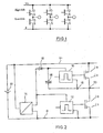
- Fig. 1 is a three-phase inverter with three half-bridges, each of which contains two MOSFETs.
- the transistors connected to positive potential V + are high-side transistors and the transistors connected to negative potential are low-side transistors.
- a motor phase is connected in each case.
- the three-phase motor such as drive or lifting motor in a truck, is not shown.
- Fig. 2 is a half bridge after Fig. 1 shown. It also recognizes electronic control circuits 10, 12 for the two transistors and a power supply 14 for the circuits 10, 12.
- the drive circuit 10 receives its power supply from a capacitor 16 which is connected via a diode 18 to the power supply 14.
- the reference potential of the drive circuit 10, as shown at 18, is at the same potential as a connection point 20 between the source of the high-side transistor and the drain of the low-side transistor and thus a phase.
- the reference potential for the control circuit 10 is the negative potential of the designated 22 battery, which supplies the three-phase motor with energy.
- the transistors are alternately switched by the control circuits 10, 12. As a result, the potential of the points 18 and 20 jumps between positive and negative power supply back and forth.
- the capacitor 16 can only be charged when the low-side transistor on and the high-side transistor is turned off. Then, the current from the power supply 14 via the diode 18, the capacitor 16 charge. If the high-side transistor is switched on and the low-side transistor is switched off, the "jumping reference potential" 18 is at the potential of the positive current supply.
- the control circuit 10 can be powered only from the capacitor 16, because diode 18 is in the off state. This is called pumping because charge is "pumped" from a low potential to a higher one.
- a three-phase motor 24 which is located on a phase of the inverter, wherein a Meßshunt 26 is provided for the current measurement in the phase.
- the current measurement is carried out with the aid of a measuring amplifier 28.
- the reference potential for the measuring amplifier 28 and the measuring inputs of the amplifier 28 change with the potential at the point 20.
- the supply of the measuring amplifier 28 takes place via the terminal 20 or a capacitor 30 which is charged via a diode 32.
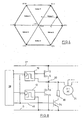
- Fig. 4 the space vector diagram of a space vector modulation is shown.
- the control of the high-side transistor is indicated by the numeral 1 and that of the low-side transistor by the numeral 0.
- the state of the inverter with its three phases can then be specified as a triple, z. B. 0 0 1. Since the three phases of a three-phase current on a circle shifted by 120 ° spatially can be shown as a pointer, resulting for the individual switching states of the inverter after Fig. 1 six vectors, also called base vectors, that span a regular hexagon. Two states, namely activation of all high-side or low-side transistors (1 1 1 or 0 0 0) are referred to as zero vectors. Between the basis vectors are six sectors which are in Fig. 4 are designated accordingly.
- Phase 9 shows the voltage curve of the phase in which the carrier frequency has been filtered and in which the voltage vector the inner circle of the in Fig. 4 hexes shown follows.
- Phases 2 and 3 are phase shifted by 120 °.
- the example describes the harmonic control of the three-phase motor with maximum amplitude.
- Fig. 10 shows the voltage curve of phase 1 accordingly Fig. 9 but in the method according to the invention.
- auxiliary transistor 34 which is connected between connection point 20 and negative potential and a resistor 36 is connected in series, is also supplied by a control electronics 38 for the control circuits 10 and 12 for the half-bridge shown with a blocking signal via a line 40 when the inverter locked becomes.
- the blocking signal activates the auxiliary transistor 34 and generates a potential at point 20 which, for example, lies at half of the positive current supply V +.
- This potential serves as a reference potential for the control circuit 10 and the in Fig. 8 not shown measuring amplifier (see position 28 after Fig. 3 ).
- the storage capacitors of the charge pumps are charged.
Landscapes
- Engineering & Computer Science (AREA)
- Power Engineering (AREA)
- Inverter Devices (AREA)
- Control Of Ac Motors In General (AREA)
Claims (2)
- Procédé destiné à faire fonctionner un commutateur de courant triphasé, qui présente respectivement au moins deux transistors de puissance dans trois demi-ponts en vue de générer un courant triphasé à partir d'un courant continu pour des moteurs à courant triphasé, en particulier dans des chariots de manutention, dans lequel en vue de générer n'importe quelles valeurs voltmétriques, les transistors de puissance sont commutés après la modulation du pointeur d'espace avec fréquence porteuse élevée à la manière de la modulation d'impulsions en largeur symétrique (PWM) au cours de la durée de période de la porteuse entre deux vecteurs de base consécutifs et un vecteur nul d'un secteur, dans les secteurs impairs, les vecteurs de base sont appliqués dans un premier sens de rotation et dans les secteurs pairs dans le sens de rotation opposé de telle manière que le vecteur nul n'est généré que via mise sous tension des transistors se trouvant au niveau du potentiel négatif, caractérisé en ce que l'alimentation en courant de l'électronique (10) des transistors est effectuée à l'aide d'une pompe de charge comportant un condensateur (16) et une diode (18), et à l'aide du signal de blocage pour tous les transistors est amorcé un transistor auxiliaire (34) qui relie un point de jonction (20) entre les transistors d'un demi-pont avec le potentiel négatif par l'intermédiaire d'une résistance de limitation (36)
- Procédé selon la revendication 1, dans lequel l'alimentation en courant d'un amplificateur de mesure (28) relié à un shunt (26) dans une phase est effectuée à l'aide d'une pompe de charge comportant un condensateur (30) et une diode (32), et à l'aide du signal de blocage pour tous les transistors est amorcé un transistor auxiliaire (34) qui relie un point de jonction (20) entre les transistors d'un demi-pont avec le potentiel négatif par l'intermédiaire d'une résistance de limitation (36).
Applications Claiming Priority (2)
| Application Number | Priority Date | Filing Date | Title |
|---|---|---|---|
| DE1999110327 DE19910327C2 (de) | 1999-03-09 | 1999-03-09 | Verfahren zum Betrieb eines Drehstromumrichters für Drehstrommotoren |
| DE19910327 | 1999-03-09 |
Publications (3)
| Publication Number | Publication Date |
|---|---|
| EP1035642A1 EP1035642A1 (fr) | 2000-09-13 |
| EP1035642B1 EP1035642B1 (fr) | 2007-06-20 |
| EP1035642B2 true EP1035642B2 (fr) | 2013-03-27 |
Family
ID=7900241
Family Applications (1)
| Application Number | Title | Priority Date | Filing Date |
|---|---|---|---|
| EP00100094A Expired - Lifetime EP1035642B2 (fr) | 1999-03-09 | 2000-01-07 | Modulation de largeur d'impulsion pour contrôler un onduleur pour moteur AC |
Country Status (2)
| Country | Link |
|---|---|
| EP (1) | EP1035642B2 (fr) |
| DE (2) | DE19910327C2 (fr) |
Families Citing this family (8)
| Publication number | Priority date | Publication date | Assignee | Title |
|---|---|---|---|---|
| DE10102344A1 (de) * | 2001-01-19 | 2002-08-01 | Bosch Gmbh Robert | Verfahren zur Messung des Stromes in Halbbrücken |
| DE102006042384B4 (de) * | 2006-09-08 | 2008-09-11 | Siemens Ag | Umrichter und Verfahren zur Steuerung eines Umrichters |
| EP2028756A1 (fr) * | 2007-08-23 | 2009-02-25 | Siemens Aktiengesellschaft | Inverseur doté d'une protection contre les courts-circuits |
| DE102009045052B4 (de) | 2008-09-30 | 2013-04-04 | Infineon Technologies Ag | Bereitstellen einer Versorgungsspannung für eine Ansteuerschaltung eines Halbleiterschaltelements |
| DE102008049677B4 (de) | 2008-09-30 | 2014-09-18 | Infineon Technologies Ag | Spannungsversorgung in einer Schaltungsanordnung mit einem Halbleiterschaltelement |
| DE102008049673B4 (de) | 2008-09-30 | 2011-04-28 | Infineon Technologies Ag | Schaltungsanordnung mit einem Leistungshalbleitermodul und einer außerhalb dessen angeordneten Steuerschaltung |
| DE102016112815A1 (de) | 2016-07-13 | 2018-01-18 | Jungheinrich Aktiengesellschaft | Steuerung eines Drehstrommotors mit einem Kennlinienfeld sowie Verfahren zur Bestimmung desselben |
| DE102024120649A1 (de) * | 2024-07-19 | 2026-01-22 | Jungheinrich Aktiengesellschaft | Verfahren zum Betreiben einer mindestens dreiphasigen Induktionsmaschine und Induktionsmaschine |
Family Cites Families (2)
| Publication number | Priority date | Publication date | Assignee | Title |
|---|---|---|---|---|
| JP2634306B2 (ja) * | 1990-08-08 | 1997-07-23 | 三菱電機株式会社 | インバータ装置の駆動回路 |
| DK172570B1 (da) * | 1995-01-23 | 1999-01-25 | Danfoss As | Vekselretter og fremgangsmåde til måling af vekselretterens fasestrømme |
-
1999
- 1999-03-09 DE DE1999110327 patent/DE19910327C2/de not_active Expired - Lifetime
-
2000
- 2000-01-07 DE DE50014420T patent/DE50014420D1/de not_active Expired - Lifetime
- 2000-01-07 EP EP00100094A patent/EP1035642B2/fr not_active Expired - Lifetime
Non-Patent Citations (1)
| Title |
|---|
| "dsp in motion control", 9 June 1997, PCIM INT. CONF., NURNBERG, pages: SEMINAR6, PCIM † |
Also Published As
| Publication number | Publication date |
|---|---|
| EP1035642B1 (fr) | 2007-06-20 |
| DE50014420D1 (de) | 2007-08-02 |
| DE19910327C2 (de) | 2001-11-22 |
| DE19910327A1 (de) | 2000-09-21 |
| EP1035642A1 (fr) | 2000-09-13 |
Similar Documents
| Publication | Publication Date | Title |
|---|---|---|
| DE69210487T2 (de) | Leistungswandlervorrichtung mit Inverterschaltkreis zum Antrieb eines Drehstrommotors variabler Geschwindigkeit | |
| EP2297842B1 (fr) | Procédé, agencement de commutation et circuit en pont | |
| EP2348627A1 (fr) | Convertisseur et procédé pour l'operation d'un circuit convertisseur à plusieurs niveaux | |
| DE102016106359A1 (de) | Modul für einen Multilevelkonverter | |
| DE112017003632T5 (de) | Dc/dc-umrichter | |
| DE102014103454A1 (de) | System und Verfahren für einen Schaltleistungswandler | |
| EP1073192A2 (fr) | Dispositif de contrôle d'une charge à courant alternatif , en particulier d'un moteur à courant alternatif avec contrôle de vitesse | |
| DE112018006822T5 (de) | Leistungsumwandlungsvorrichtung, motormodul und elektrische servolenkvorrichtung | |
| DE102019102777A1 (de) | Pulsweitenmodulations-Mustergenerator und entsprechende Systeme, Verfahren und Computerprogramme | |
| EP0024300A1 (fr) | Procédé pour le contrôle de la durée d'impulsion d'un régulateur inverseur à courant continu et circuit pour la mise en oeuvre dudit procédé | |
| EP1035642B2 (fr) | Modulation de largeur d'impulsion pour contrôler un onduleur pour moteur AC | |
| DE10156939A1 (de) | Schaltungsanordnung zum Betreiben einer elektrischenMaschine | |
| DE112005000294T5 (de) | Motorantriebsvorrichtung | |
| EP0929932B1 (fr) | Circuit de commande pour moteur a courant continu | |
| WO2014206696A1 (fr) | Onduleur à z-source à rendement optimisé | |
| DE2750720C2 (de) | Anordnung zur Verringerung der Steuerleistung einer Leistungsschalttransistorendstufe für sehr hohe Taktfrequenz | |
| DE2050787B2 (de) | Brueckenwechselrichter mit gleichstromkommutierung | |
| DD146227A5 (de) | Schaltung fuer einen buerstenlosen gleichstrommotor | |
| WO2013092043A2 (fr) | Circuit convertisseur de courant | |
| EP2409394B1 (fr) | Procédé de fonctionnement d'un circuit convertisseur et dispositif pour la mise en uvre du procédé | |
| DE102020126054A1 (de) | Ansteuerschaltkreis für einen Elektromotor mit einstellbarer Zwischenkreisspannung und entsprechendes Verfahren zum Ansteuern eines Elektromotors | |
| DE102021103205A1 (de) | Zuführen von elektrischer Energie von einem Wechselspannungsnetz zu einem Gleichspannungsnetz | |
| DE3020745C2 (de) | Fremdgesteuerter Gleichspannungswandler | |
| EP2375551B1 (fr) | Procédé de commutation, circuit de commutation et convertisseur d'énergie électrique | |
| EP2544350B1 (fr) | Commuting method, commuting circuit and electrical energy converter |
Legal Events
| Date | Code | Title | Description |
|---|---|---|---|
| PUAI | Public reference made under article 153(3) epc to a published international application that has entered the european phase |
Free format text: ORIGINAL CODE: 0009012 |
|
| AK | Designated contracting states |
Kind code of ref document: A1 Designated state(s): DE FR GB IT SE |
|
| AX | Request for extension of the european patent |
Free format text: AL;LT;LV;MK;RO;SI |
|
| 17P | Request for examination filed |
Effective date: 20010112 |
|
| AKX | Designation fees paid |
Free format text: DE FR GB IT SE |
|
| GRAP | Despatch of communication of intention to grant a patent |
Free format text: ORIGINAL CODE: EPIDOSNIGR1 |
|
| GRAS | Grant fee paid |
Free format text: ORIGINAL CODE: EPIDOSNIGR3 |
|
| GRAA | (expected) grant |
Free format text: ORIGINAL CODE: 0009210 |
|
| AK | Designated contracting states |
Kind code of ref document: B1 Designated state(s): DE FR GB IT SE |
|
| REG | Reference to a national code |
Ref country code: GB Ref legal event code: FG4D Free format text: NOT ENGLISH |
|
| REF | Corresponds to: |
Ref document number: 50014420 Country of ref document: DE Date of ref document: 20070802 Kind code of ref document: P |
|
| GBT | Gb: translation of ep patent filed (gb section 77(6)(a)/1977) |
Effective date: 20070903 |
|
| REG | Reference to a national code |
Ref country code: SE Ref legal event code: TRGR |
|
| ET | Fr: translation filed | ||
| PLBI | Opposition filed |
Free format text: ORIGINAL CODE: 0009260 |
|
| PLAX | Notice of opposition and request to file observation + time limit sent |
Free format text: ORIGINAL CODE: EPIDOSNOBS2 |
|
| 26 | Opposition filed |
Opponent name: DIEHL AKO STIFTUNG & CO. KG Effective date: 20080320 |
|
| PLAF | Information modified related to communication of a notice of opposition and request to file observations + time limit |
Free format text: ORIGINAL CODE: EPIDOSCOBS2 |
|
| PLBB | Reply of patent proprietor to notice(s) of opposition received |
Free format text: ORIGINAL CODE: EPIDOSNOBS3 |
|
| PLAB | Opposition data, opponent's data or that of the opponent's representative modified |
Free format text: ORIGINAL CODE: 0009299OPPO |
|
| R26 | Opposition filed (corrected) |
Opponent name: DIEHL AKO STIFTUNG & CO. KG Effective date: 20080320 |
|
| PGFP | Annual fee paid to national office [announced via postgrant information from national office to epo] |
Ref country code: FR Payment date: 20120201 Year of fee payment: 13 |
|
| PGFP | Annual fee paid to national office [announced via postgrant information from national office to epo] |
Ref country code: SE Payment date: 20120124 Year of fee payment: 13 Ref country code: GB Payment date: 20120124 Year of fee payment: 13 Ref country code: IT Payment date: 20120125 Year of fee payment: 13 |
|
| PUAH | Patent maintained in amended form |
Free format text: ORIGINAL CODE: 0009272 |
|
| STAA | Information on the status of an ep patent application or granted ep patent |
Free format text: STATUS: PATENT MAINTAINED AS AMENDED |
|
| 27A | Patent maintained in amended form |
Effective date: 20130327 |
|
| AK | Designated contracting states |
Kind code of ref document: B2 Designated state(s): DE FR GB IT SE |
|
| REG | Reference to a national code |
Ref country code: DE Ref legal event code: R102 Ref document number: 50014420 Country of ref document: DE Effective date: 20130327 |
|
| REG | Reference to a national code |
Ref country code: SE Ref legal event code: NAV |
|
| GBPC | Gb: european patent ceased through non-payment of renewal fee |
Effective date: 20130107 |
|
| REG | Reference to a national code |
Ref country code: FR Ref legal event code: ST Effective date: 20130930 |
|
| PG25 | Lapsed in a contracting state [announced via postgrant information from national office to epo] |
Ref country code: FR Free format text: LAPSE BECAUSE OF NON-PAYMENT OF DUE FEES Effective date: 20130131 Ref country code: GB Free format text: LAPSE BECAUSE OF NON-PAYMENT OF DUE FEES Effective date: 20130107 |
|
| PG25 | Lapsed in a contracting state [announced via postgrant information from national office to epo] |
Ref country code: IT Free format text: LAPSE BECAUSE OF NON-PAYMENT OF DUE FEES Effective date: 20130107 |
|
| PG25 | Lapsed in a contracting state [announced via postgrant information from national office to epo] |
Ref country code: SE Free format text: LAPSE BECAUSE OF NON-PAYMENT OF DUE FEES Effective date: 20130108 |
|
| PGFP | Annual fee paid to national office [announced via postgrant information from national office to epo] |
Ref country code: DE Payment date: 20180329 Year of fee payment: 19 |
|
| REG | Reference to a national code |
Ref country code: DE Ref legal event code: R119 Ref document number: 50014420 Country of ref document: DE |
|
| PG25 | Lapsed in a contracting state [announced via postgrant information from national office to epo] |
Ref country code: DE Free format text: LAPSE BECAUSE OF NON-PAYMENT OF DUE FEES Effective date: 20190801 |