EP1035642B2 - Pulse width modulation for driving an inverter for AC motors - Google Patents
Pulse width modulation for driving an inverter for AC motors Download PDFInfo
- Publication number
- EP1035642B2 EP1035642B2 EP00100094A EP00100094A EP1035642B2 EP 1035642 B2 EP1035642 B2 EP 1035642B2 EP 00100094 A EP00100094 A EP 00100094A EP 00100094 A EP00100094 A EP 00100094A EP 1035642 B2 EP1035642 B2 EP 1035642B2
- Authority
- EP
- European Patent Office
- Prior art keywords
- transistors
- phase
- bridge
- coupling point
- inverter
- Prior art date
- Legal status (The legal status is an assumption and is not a legal conclusion. Google has not performed a legal analysis and makes no representation as to the accuracy of the status listed.)
- Expired - Lifetime
Links
Images


Classifications
-
- H—ELECTRICITY
- H02—GENERATION; CONVERSION OR DISTRIBUTION OF ELECTRIC POWER
- H02M—APPARATUS FOR CONVERSION BETWEEN AC AND AC, BETWEEN AC AND DC, OR BETWEEN DC AND DC, AND FOR USE WITH MAINS OR SIMILAR POWER SUPPLY SYSTEMS; CONVERSION OF DC OR AC INPUT POWER INTO SURGE OUTPUT POWER; CONTROL OR REGULATION THEREOF
- H02M7/00—Conversion of ac power input into dc power output; Conversion of dc power input into ac power output
- H02M7/42—Conversion of dc power input into ac power output without possibility of reversal
- H02M7/44—Conversion of dc power input into ac power output without possibility of reversal by static converters
- H02M7/48—Conversion of dc power input into ac power output without possibility of reversal by static converters using discharge tubes with control electrode or semiconductor devices with control electrode
- H02M7/53—Conversion of dc power input into ac power output without possibility of reversal by static converters using discharge tubes with control electrode or semiconductor devices with control electrode using devices of a triode or transistor type requiring continuous application of a control signal
- H02M7/537—Conversion of dc power input into ac power output without possibility of reversal by static converters using discharge tubes with control electrode or semiconductor devices with control electrode using devices of a triode or transistor type requiring continuous application of a control signal using semiconductor devices only, e.g. single switched pulse inverters
- H02M7/5387—Conversion of dc power input into ac power output without possibility of reversal by static converters using discharge tubes with control electrode or semiconductor devices with control electrode using devices of a triode or transistor type requiring continuous application of a control signal using semiconductor devices only, e.g. single switched pulse inverters in a bridge configuration
- H02M7/53871—Conversion of dc power input into ac power output without possibility of reversal by static converters using discharge tubes with control electrode or semiconductor devices with control electrode using devices of a triode or transistor type requiring continuous application of a control signal using semiconductor devices only, e.g. single switched pulse inverters in a bridge configuration with automatic control of output voltage or current
- H02M7/53875—Conversion of dc power input into ac power output without possibility of reversal by static converters using discharge tubes with control electrode or semiconductor devices with control electrode using devices of a triode or transistor type requiring continuous application of a control signal using semiconductor devices only, e.g. single switched pulse inverters in a bridge configuration with automatic control of output voltage or current with analogue control of three-phase output
Definitions
- the invention relates to a method for operating a three-phase converter according to the preamble of patent claim 1.
- the power section of a three-phase converter or inverter usually consists of three bridge arrangements with power transistors, usually of the type MOS or IGBT.
- Each bridge includes one transistor or a plurality of parallel connected transistors connected to the positive potential and one or a plurality of transistors connected in parallel and connected to the negative potential.
- the former are referred to as high-side transistors and the latter as low-side transistors.
- a three-phase phase is connected to the connection between a high-side and a low-side transistor.
- the drive electronics for the power transistors requires a reference potential.
- Another possibility is to provide a so-called charge pump.
- the control of the low-side transistors can be done easily because they have the same negative power supply as reference potential as the control part and the power supply for this purpose.
- the reference potential for driving the high-side transistors is their source or emitter terminal, which is connected to the drain or collector terminal of the low-side transistors and forms with possibly interposed Strommeßshunt the connection of a motor phase. Due to the fast switching operations of the transistors, the reference potential of the high-side transistors of each bridge arrangement jumps between the potentials of the negative and positive current supply. The same applies to the reference potential and the measuring inputs of the current measuring amplifier. Without special circuit measures a control and supply of the measuring amplifier from a power supply with a fixed reference potential is not possible.
- the invention is based on the object Specify method for operating a three-phase converter according to the space vector modulation, in which all the transistors and the sense amplifier of a current measuring shunt from a control electronics and power supply without potential isolation can be controlled or supplied.
- the base vectors are applied in a first direction of rotation and in the even-numbered sectors in the opposite direction of rotation such that the zero vector is generated only by turning on the negative-potential transistors.
- the inventive method ensures that the zero vector is generated by turning on all low-side transistors. In this way, the advantageous supply of electronics with "jumping potentials" by “pumping” of charge by means of a charge pump formed of storage capacitor and diode, has become possible.
- the jumping reference terminal of the capacitors of the charge pumps which is connected to the motor phase, in the case of the locked inverter by an auxiliary transistor to the potential of the negative power supply is set.
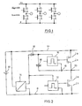
- Fig. 1 is a three-phase inverter with three half-bridges, each of which contains two MOSFETs.
- the transistors connected to positive potential V + are high-side transistors and the transistors connected to negative potential are low-side transistors.
- a motor phase is connected in each case.
- the three-phase motor such as drive or lifting motor in a truck, is not shown.
- Fig. 2 is a half bridge after Fig. 1 shown. It also recognizes electronic control circuits 10, 12 for the two transistors and a power supply 14 for the circuits 10, 12.
- the drive circuit 10 receives its power supply from a capacitor 16 which is connected via a diode 18 to the power supply 14.
- the reference potential of the drive circuit 10, as shown at 18, is at the same potential as a connection point 20 between the source of the high-side transistor and the drain of the low-side transistor and thus a phase.
- the reference potential for the control circuit 10 is the negative potential of the designated 22 battery, which supplies the three-phase motor with energy.
- the transistors are alternately switched by the control circuits 10, 12. As a result, the potential of the points 18 and 20 jumps between positive and negative power supply back and forth.
- the capacitor 16 can only be charged when the low-side transistor on and the high-side transistor is turned off. Then, the current from the power supply 14 via the diode 18, the capacitor 16 charge. If the high-side transistor is switched on and the low-side transistor is switched off, the "jumping reference potential" 18 is at the potential of the positive current supply.
- the control circuit 10 can be powered only from the capacitor 16, because diode 18 is in the off state. This is called pumping because charge is "pumped" from a low potential to a higher one.
- a three-phase motor 24 which is located on a phase of the inverter, wherein a Meßshunt 26 is provided for the current measurement in the phase.
- the current measurement is carried out with the aid of a measuring amplifier 28.
- the reference potential for the measuring amplifier 28 and the measuring inputs of the amplifier 28 change with the potential at the point 20.
- the supply of the measuring amplifier 28 takes place via the terminal 20 or a capacitor 30 which is charged via a diode 32.
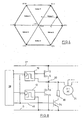
- Fig. 4 the space vector diagram of a space vector modulation is shown.
- the control of the high-side transistor is indicated by the numeral 1 and that of the low-side transistor by the numeral 0.
- the state of the inverter with its three phases can then be specified as a triple, z. B. 0 0 1. Since the three phases of a three-phase current on a circle shifted by 120 ° spatially can be shown as a pointer, resulting for the individual switching states of the inverter after Fig. 1 six vectors, also called base vectors, that span a regular hexagon. Two states, namely activation of all high-side or low-side transistors (1 1 1 or 0 0 0) are referred to as zero vectors. Between the basis vectors are six sectors which are in Fig. 4 are designated accordingly.
- Phase 9 shows the voltage curve of the phase in which the carrier frequency has been filtered and in which the voltage vector the inner circle of the in Fig. 4 hexes shown follows.
- Phases 2 and 3 are phase shifted by 120 °.
- the example describes the harmonic control of the three-phase motor with maximum amplitude.
- Fig. 10 shows the voltage curve of phase 1 accordingly Fig. 9 but in the method according to the invention.
- auxiliary transistor 34 which is connected between connection point 20 and negative potential and a resistor 36 is connected in series, is also supplied by a control electronics 38 for the control circuits 10 and 12 for the half-bridge shown with a blocking signal via a line 40 when the inverter locked becomes.
- the blocking signal activates the auxiliary transistor 34 and generates a potential at point 20 which, for example, lies at half of the positive current supply V +.
- This potential serves as a reference potential for the control circuit 10 and the in Fig. 8 not shown measuring amplifier (see position 28 after Fig. 3 ).
- the storage capacitors of the charge pumps are charged.
Description
Die Erfindung bezieht sich auf ein Verfahren zum Betrieb eines Drehstromumrichters nach dem Oberbegriff des Patentanspruchs 1.The invention relates to a method for operating a three-phase converter according to the preamble of
Der Leistungsteil eines Drehstromumrichters oder -wechselrichters besteht üblicherweise aus drei Brückenanordnungen mit Leistungstransistoren, zumeist des Typs MOS oder IGBT. Jede Brücke enthält einen Transistor oder eine Mehrzahl parallelgeschalteter Transistoren, welche mit dem positiven Potential und einen Transistor oder eine Mehrzahl von parallelgeschalteten Transistoren, welche mit dem negativen Potential verbunden sind. Erstere werden als High-Side-Transistoren und letztere als Low-Side-Transistoren bezeichnet. Jeweils eine Drehstromphase ist an der Verbindung zwischen einem High-Side- und einem Low-Side-Transistor angeschlossen.The power section of a three-phase converter or inverter usually consists of three bridge arrangements with power transistors, usually of the type MOS or IGBT. Each bridge includes one transistor or a plurality of parallel connected transistors connected to the positive potential and one or a plurality of transistors connected in parallel and connected to the negative potential. The former are referred to as high-side transistors and the latter as low-side transistors. In each case, a three-phase phase is connected to the connection between a high-side and a low-side transistor.
Die Ansteuerungselektronik für die Leistungstransistoren benötigt ein Bezugspotential. Das gleiche trifft auf einen Meßverstärker zu, der mit dem Shunt in einer Phase verbunden ist zur Messung des zum Motor fließenden Stroms für die Regelung. Es ist bekannt, die Versorgung und Ansteuerung dieser Baugruppen durch Potentialtrennung vorzunehmen. Hierfür ist ein hoher Aufwand erforderlich.The drive electronics for the power transistors requires a reference potential. The same applies to a sense amplifier which is connected to the shunt in a phase for measuring the current flowing to the motor for the control. It is known to make the supply and control of these modules by electrical isolation. This requires a lot of effort.
Eine andere Möglichkeit besteht darin, eine sogenannte Ladungspumpe vorzusehen.Another possibility is to provide a so-called charge pump.
Die Ansteuerung der Low-Side-Transistoren kann problemlos erfolgen, weil diese die gleiche negative Stromzuführung als Bezugspotential aufweisen wie der Steuerteil und die Stromversorgung hierfür. Ein Problem entsteht jedoch bei der Ansteuerung der High-Side-Transistoren und der Ansteuerung bzw. Versorgung des Meßverstärkers für den Strom. Das Bezugspotential zur Ansteuerung der High-Side-Transistoren ist deren Source bzw. Emitteranschluß, welcher mit dem Drain- bzw. Kollektoranschluß der Low-Side-Transistoren verbunden ist und mit ggf. zwischengeschaltetem Strommeßshunt den Anschluß einer Motorphase bildet. Aufgrund der schnellen Schaltvorgänge der Transistoren springt das Bezugspotential der High-Side-Transistoren einer jeden Brückenanordnung zwischen den Potentialen der negativen und positiven Stromzuführung hin und her. Das gleiche betrifft das Bezugspotential und die Meßeingänge des Strommeßverstärkers. Ohne besondere Schaltungsmaßnahmen ist eine Ansteuerung und Versorgung des Meßverstärkers aus einer Stromversorgung mit festem Bezugspotential nicht möglich.The control of the low-side transistors can be done easily because they have the same negative power supply as reference potential as the control part and the power supply for this purpose. However, a problem arises in the control of the high-side transistors and the control or supply of the measuring amplifier for the current. The reference potential for driving the high-side transistors is their source or emitter terminal, which is connected to the drain or collector terminal of the low-side transistors and forms with possibly interposed Strommeßshunt the connection of a motor phase. Due to the fast switching operations of the transistors, the reference potential of the high-side transistors of each bridge arrangement jumps between the potentials of the negative and positive current supply. The same applies to the reference potential and the measuring inputs of the current measuring amplifier. Without special circuit measures a control and supply of the measuring amplifier from a power supply with a fixed reference potential is not possible.
Ein Umrichter der beschriebenen Art soll mit Hilfe der geschalteten Transistoren einen kontinuierlichen Spannungsverlauf erzeugen. Dazu bedarf es eines Modulationsverfahrens, das die Transistoren in einer hohen Trägerfrequenz schaltet, beispielsweise 16 kHz, um in einem unteren Frequenzbereich ein kontinuierliches Nutzsignal zu erzeugen, beispielsweise ein Nutzsignal von 50 Hz Sinus. Die Anforderungen an das Modulationsverfahren sind:
- Variable Spannung mit möglichst guter Ausnutzung der Betriebsspannung
- Variable Frequenz einschließlich Gleichspannung
- Beliebige, auch nicht sinusförmige Signalformen
- Geringe Schalthäufigkeit, um Umschaltverluste kleiner zu halten.
- Variable voltage with the best possible utilization of the operating voltage
- Variable frequency including DC voltage
- Any, not sinusoidal waveforms
- Low switching frequency to keep switching losses smaller.
Ein Modulationsverfahren, das diesen Anforderungen genügt, ist die bekannte Raumzeigermodulation. Außer im Fall eines vollständig gesperrten Wechselrichters lassen sich mit dem beschriebenen Umrichter 23 = 8 verschiedene Schaltzustände herstellen, in denen entweder ein High-Side-Transistor oder ein Low-Side-Transistor aktiv ist. Wenn die drei Phasen auf einem Kreis um jeweils 120° räumlich verschoben angeordnet sind, lassen sich die Schaltzustände durch Spannungsraumzeiger darstellen. Zwei Zustände, in denen entweder die High-Side- oder die Low-Side-Transistoren alle aktiv sind, werden als Nullvektoren bezeichnet. Die anderen sechs Vektoren, die Basisvektoren, spannen ein regelmäßiges Sechseck auf.One modulation method which satisfies these requirements is known space vector modulation. Except in the case of a fully locked
Um einen beliebigen Spannungswert innerhalb des Sechsecks zu erzeugen, wird nach Art der symmetrischen Pulsweitenmodulation innerhalb der Trägerperiodendauer zwischen benachbarten Basisvektoren und einem Nullvektor umgeschaltet. Bei diesem Verfahren wird bei jedem Schaltvorgang nur eine Halbbrücke umgeschaltet, was zu geringen Schaltverlusten führt. Der Artikel "
Weiterhin besteht das Problem, daß wenn alle Transistoren gesperrt sind, dies auch für die Low-Side-Transistoren gilt. In diesem Fall können die Kondensatoren der Ladungspumpen der High-Side-Ansteuerelektronik und des Strommeßverstärkers nicht aufgeladen werden. Nach Freigabe des Wechselrichters wird daher der Strommeßverstärker nicht sofort versorgt. Dies hat zur Folge, daß ein gefordertes Anfahrmoment nicht sofort zur Verfügung steht.Furthermore, there is the problem that when all transistors are disabled, this also applies to the low-side transistors. In this case, the capacitors of the charge pumps of the high-side drive electronics and the current measuring amplifier can not be charged. After release of the inverter, therefore, the current measuring amplifier is not supplied immediately. This has the consequence that a required starting torque is not immediately available.
Schließlich besteht die Gefahr der Zerstörung von High-Side-Transistoren, deren Ansteuerelektronik aufgrund der besonderen Modulation nicht sofort versorgt werden kann (Raumzeigermodulation mit Schaltpausen während 60° eines Zyklus).Finally, there is the danger of destruction of high-side transistors whose control electronics can not be supplied immediately due to the special modulation (space vector modulation with switching pauses during 60 ° of a cycle).
Aus der Seminarunterlagen der Konferenz, PCIM International Conference, Nürnberg 1997, SEMINAR NOTES, Seminar 6, "DSP IN MOTION CONTROL" ist ein Verfahren mit Merkmalen des Oberbegriffes des Anspruchs 1 bekannt geworden.From the seminar documents of the conference, PCIM International Conference, Nuremberg 1997, SEMINAR NOTES,
Der Erfindung liegt die Aufgabe zugrunde, ein Verfahren zum Betrieb eines Drehstromumrichters nach der Raumzeigermodulation anzugeben, bei dem alle Transistoren und der Meßverstärker eines Strommeßshunts aus einer Steuerelektronik und Stromversorgung ohne Potentialtrennung angesteuert bzw. versorgt werden können.The invention is based on the object Specify method for operating a three-phase converter according to the space vector modulation, in which all the transistors and the sense amplifier of a current measuring shunt from a control electronics and power supply without potential isolation can be controlled or supplied.
Diese Aufgabe wird durch die Merkmale des Patentanspruchs 1 gelöst.This object is solved by the features of
Bei dem erfindungsgemäßen Verfahren werden in den ungeradzahligen Sektoren des Zeigerdiagramms die Basisvektoren in einer ersten Drehrichtung und in den geradzahligen Sektoren in der entgegengesetzten Drehrichtung angelegt derart, daß der Nullvektor nur durch Einschalten der an Minuspotential liegenden Transistoren erzeugt wird. Durch das erfindungsgemäße Verfahren ist sichergestellt, daß der Nullvektor durch das Einschalten aller Low-Side-Transistoren erzeugt wird. Auf diese Weise ist die vorteilhafte Versorgung von Elektroniken mit "springenden Potentialen" durch "Pumpen" von Ladung mittels einer Ladungspumpe, gebildet aus Speicherkondensator und Diode, möglich geworden.In the method according to the invention, in the odd-numbered sectors of the phasor diagram, the base vectors are applied in a first direction of rotation and in the even-numbered sectors in the opposite direction of rotation such that the zero vector is generated only by turning on the negative-potential transistors. The inventive method ensures that the zero vector is generated by turning on all low-side transistors. In this way, the advantageous supply of electronics with "jumping potentials" by "pumping" of charge by means of a charge pump formed of storage capacitor and diode, has become possible.
Bei der Erfindung ist der springende Bezugsleiteranschluß der Kondensatoren der Ladungspumpen, der mit der Motorphase verbunden ist, im Fall des gesperrten Wechselrichters durch einen Hilfstransistor auf das Potential der negativen Stromführung gelegt.In the invention, the jumping reference terminal of the capacitors of the charge pumps, which is connected to the motor phase, in the case of the locked inverter by an auxiliary transistor to the potential of the negative power supply is set.
Die Erfindung wird nachfolgend anhand von in Zeichnungen dargestellten Ausführungsbeispielen näher erläutert.
- Fig. 1
- zeigt einen Wechselstrom-Umrichter mit drei Halbbrücken.
- Fig. 2
- zeigt eine Halbbrücke nach
Fig. 1 mit dem Prinzipschaltbild einer Ladungspumpe. - Fig. 3
- zeigt eine Halbbrücke nach
Fig. 1 mit Ladungspumpe und einem Strommeßverstärker. - Fig. 4
- zeigt ein Raumzeigerdiagramm einer Raumzeigermodulation für einen Umformer nach
Fig. 1 . - Fig. 5
- zeigt ein Diagramm für die Raumzeigermodulation im
Sektor 1 nachFig. 4 . - Fig. 6
- zeigt eine Raumzeigermodulation in
Sektor 2 nachFig. 4 . - Fig. 7
- zeigt eine erfindungsgemäße Modulation in
Sektor 1 nachFig. 4 . - Fig. 8
- zeigt ein ähnliches Schaltbild wie
Fig. 1 , jedoch mit einem zusätzlichen Schaltungsteil. - Fig. 9
- zeigt das Diagramm einer gefilterten Ausgangsspannung einer Phase des Umrichters nach
Fig. 1 mit einer Raumzeigermodulation nachFig. 5 .und 6 - Fig. 10
- zeigt die gefilterte Ausgangsspannung einer Phase nach der erfindungsgemäßen Modulation.
- Fig. 1
- shows an AC inverter with three half-bridges.
- Fig. 2
- shows a half-bridge after
Fig. 1 with the schematic diagram of a charge pump. - Fig. 3
- shows a half-bridge after
Fig. 1 with charge pump and a current measuring amplifier. - Fig. 4
- Figure 12 shows a space vector diagram of space vector modulation for a converter
Fig. 1 , - Fig. 5
- shows a diagram for space vector modulation in
sector 1Fig. 4 , - Fig. 6
- shows space vector modulation in
sector 2Fig. 4 , - Fig. 7
- shows a modulation according to the invention in
sector 1Fig. 4 , - Fig. 8
- shows a similar circuit diagram as
Fig. 1 , but with an additional circuit part. - Fig. 9
- shows the diagram of a filtered output voltage of a phase of the inverter
Fig. 1 with a space vector modulation afterFIGS. 5 and 6 , - Fig. 10
- shows the filtered output voltage of one phase after the modulation according to the invention.
In
In
Die Transistoren werden durch die Steuerschaltungen 10, 12 wechselweise geschaltet. Dadurch springt das Potential der Punkte 18 bzw. 20 zwischen positiver und negativer Stromzuführung hin und her. Der Kondensator 16 kann nur aufgeladen werden, wenn der Low-Side-Transistor ein- und der High-Side-Transistor ausgeschaltet ist. Dann kann der Strom aus der Stromversorgung 14 über die Diode 18 den Kondensator 16 aufladen. Wenn der High-Side-Transistor ein- und der Low-Side-Transistor ausgeschaltet ist, befindet sich das "springende Bezugspotential" 18 auf dem Potential der positiven Stromzuführung. Nun kann die Steuerschaltung 10 nur aus dem Kondensator 16 versorgt werden, denn Diode 18 befindet sich im Sperrzustand. Man bezeichnet dies als Pumpvorgang, weil Ladung von einem niedrigen Potential zu einem höheren "gepumpt" wird.The transistors are alternately switched by the
Soweit bei der Schaltungsanordnung nach
Aufgrund der schnellen Schaltvorgänge der Transistoren springt das Bezugspotential (springendes Potential) hin und her, so daß auch das Bezugspotential und die Meßeingänge für den Meßverstärker 28 springen. Ohne besondere Schaltungsmaßnahmen ist eine Ansteuerung und Versorgung des Meßverstärkers 28 mit festem Bezugspotential nicht möglich.Due to the rapid switching operations of the transistors, the reference potential jumps (jumping potential) back and forth, so that the reference potential and the measurement inputs jump for the
In
Um einen beliebigen Spannungswert innerhalb des Sechsecks zu erzeugen, wird bei der symmetrischen Pulsweitenmodulation innerhalb der Trägerperiodendauer zwischen benachbarten Basisvektoren und einem Nullvektor umgeschaltet. Dies ist in
Bei der Raumzeigermodulation nach der Erfindung werden gemäß
Die in
Es genügt, wenn nur mit einer Motorphase ein Hilfstransistor 34 verbunden ist. Die anderen Motorphasen haben durch die entsprechenden Wicklungsstränge des Motors Verbindung. Der Widerstand 36 hat die Aufgabe, den Strom im Umschaltaugenblick zu begrenzen.It is sufficient if only one motor phase, an auxiliary transistor 34 is connected. The other motor phases are connected by the respective winding phases of the motor. The
Claims (2)
- A method for the operation of a three-phase current inverter which has at least two power transistors each in three half-bridges, for generating a three-phase alternating current from a direct current for use in three-phase motors, particularly in industrial trucks, wherein the power transistors are switched over, for the generation of random voltage values, between two adjacent base vectors and a zero vector of a sector according to the space vector modulation of a high carrier frequency in the fashion of symmetric pulse width modulation (PWM) within the carrier period duration, wherein the base vectors are applied in a first sense of rotation in the odd-numbered sectors and in an opposite sense of rotation in the even-numbered sectors such that the zero vector is produced only by switching on the transistors located at the negative potential, characterized in that the voltage supply of a driving electronics (10) of the transistors is effected by means of a charging pump including a capacitor (16) and a diode (18), wherein the charging pump is connected to a coupling point (20) between the transistors of a half-bridge, and an inhibiting signal for all transistors helps drive an auxiliary transistor (34) which connects the coupling point (20) between the transistors of the half-bridge to the negative potential via a limiting resistor (36).
- The method according to claim 1, wherein the voltage supply of a measuring amplifier (28) connected to a shunt in one phase is performed by means of a charging pump including a capacitor (30) and a diode (32), wherein the charging pump is connected to the coupling point (20) between the transistors of a half-bridge and an inhibiting signal for all transistors helps drive an auxiliary transistor (34) which connects a coupling point between the transistors of a half-bridge to the negative potential via a limiting resistor (36).
Applications Claiming Priority (2)
| Application Number | Priority Date | Filing Date | Title |
|---|---|---|---|
| DE19910327 | 1999-03-09 | ||
| DE1999110327 DE19910327C2 (en) | 1999-03-09 | 1999-03-09 | Method for operating a three-phase converter for three-phase motors |
Publications (3)
| Publication Number | Publication Date |
|---|---|
| EP1035642A1 EP1035642A1 (en) | 2000-09-13 |
| EP1035642B1 EP1035642B1 (en) | 2007-06-20 |
| EP1035642B2 true EP1035642B2 (en) | 2013-03-27 |
Family
ID=7900241
Family Applications (1)
| Application Number | Title | Priority Date | Filing Date |
|---|---|---|---|
| EP00100094A Expired - Lifetime EP1035642B2 (en) | 1999-03-09 | 2000-01-07 | Pulse width modulation for driving an inverter for AC motors |
Country Status (2)
| Country | Link |
|---|---|
| EP (1) | EP1035642B2 (en) |
| DE (2) | DE19910327C2 (en) |
Families Citing this family (7)
| Publication number | Priority date | Publication date | Assignee | Title |
|---|---|---|---|---|
| DE10102344A1 (en) * | 2001-01-19 | 2002-08-01 | Bosch Gmbh Robert | Procedure for measuring the current in half bridges |
| DE102006042384B4 (en) | 2006-09-08 | 2008-09-11 | Siemens Ag | Inverter and method for controlling an inverter |
| EP2028756A1 (en) * | 2007-08-23 | 2009-02-25 | Siemens Aktiengesellschaft | An Inverter With Short Circuit Protection |
| DE102009045052B4 (en) | 2008-09-30 | 2013-04-04 | Infineon Technologies Ag | Providing a supply voltage for a drive circuit of a semiconductor switching element |
| DE102008049673B4 (en) | 2008-09-30 | 2011-04-28 | Infineon Technologies Ag | Circuit arrangement with a power semiconductor module and a control circuit arranged outside thereof |
| DE102008049677B4 (en) | 2008-09-30 | 2014-09-18 | Infineon Technologies Ag | Power supply in a circuit arrangement with a semiconductor switching element |
| DE102016112815A1 (en) | 2016-07-13 | 2018-01-18 | Jungheinrich Aktiengesellschaft | Control of a three-phase motor with a characteristic field and method for determining the same |
Family Cites Families (2)
| Publication number | Priority date | Publication date | Assignee | Title |
|---|---|---|---|---|
| JP2634306B2 (en) * | 1990-08-08 | 1997-07-23 | 三菱電機株式会社 | Inverter drive circuit |
| DK172570B1 (en) * | 1995-01-23 | 1999-01-25 | Danfoss As | Inverters and method for measuring the inverter phase currents |
-
1999
- 1999-03-09 DE DE1999110327 patent/DE19910327C2/en not_active Expired - Lifetime
-
2000
- 2000-01-07 EP EP00100094A patent/EP1035642B2/en not_active Expired - Lifetime
- 2000-01-07 DE DE50014420T patent/DE50014420D1/en not_active Expired - Lifetime
Non-Patent Citations (1)
| Title |
|---|
| "dsp in motion control", 9 June 1997, PCIM INT. CONF., NURNBERG, pages: SEMINAR6, PCIM † |
Also Published As
| Publication number | Publication date |
|---|---|
| DE50014420D1 (en) | 2007-08-02 |
| DE19910327C2 (en) | 2001-11-22 |
| DE19910327A1 (en) | 2000-09-21 |
| EP1035642A1 (en) | 2000-09-13 |
| EP1035642B1 (en) | 2007-06-20 |
Similar Documents
| Publication | Publication Date | Title |
|---|---|---|
| EP2297842B1 (en) | Method, circuit configuration, and bridge circuit | |
| EP2348627A1 (en) | Converter circuit and method for operating a multilevel converter circuit | |
| DE112005000294T5 (en) | Motor driving device | |
| WO2017174102A1 (en) | Module for a multilevel converter | |
| DE112017003632T5 (en) | DC / DC CONVERTER | |
| DE102014103454A1 (en) | System and method for a switching power converter | |
| EP1073192A2 (en) | Device for driving an AC load, especially an AC motor with speed control | |
| EP0024300A1 (en) | Process for pulse-width control of a direct current two-way control element and circuitry for the application of the process | |
| DE112018006822T5 (en) | POWER CONVERTER, MOTOR MODULE AND ELECTRIC POWER STEERING DEVICE | |
| DE102019102777A1 (en) | Pulse width modulation pattern generator and corresponding systems, methods and computer programs | |
| EP1035642B2 (en) | Pulse width modulation for driving an inverter for AC motors | |
| DE10156939A1 (en) | Circuit arrangement for operating an electrical machine | |
| EP0744824A1 (en) | Two-phase asynchronous motor supply circuit | |
| EP0929932B1 (en) | Control circuit for a dc motor | |
| WO2014206696A1 (en) | Z-source inverter with optimized efficiency | |
| DE102006060828A1 (en) | Inverter with a delay circuit for PWM signals | |
| DE2750720C2 (en) | Arrangement for reducing the control power of a power switching transistor output stage for a very high clock frequency | |
| DE2050787B2 (en) | BRIDGE INVERTER WITH DC COMMUTATION | |
| DE2739387A1 (en) | Vehicle electric current supply controller - has single magnetic circuit regulating two separate inductor systems | |
| WO2013092043A2 (en) | Power converter circuit | |
| DE102020126054A1 (en) | Control circuit for an electric motor with adjustable intermediate circuit voltage and corresponding method for controlling an electric motor | |
| DD146227A5 (en) | CIRCUIT FOR A BUILT-FREE DC CURRENT MOTOR | |
| EP2409394B1 (en) | Method for operating an inverter circuit and device for performing the method | |
| EP2375551B1 (en) | Commutation method, commutation circuit and electric power converter | |
| DE3020745C2 (en) | Externally controlled DC voltage converter |
Legal Events
| Date | Code | Title | Description |
|---|---|---|---|
| PUAI | Public reference made under article 153(3) epc to a published international application that has entered the european phase |
Free format text: ORIGINAL CODE: 0009012 |
|
| AK | Designated contracting states |
Kind code of ref document: A1 Designated state(s): DE FR GB IT SE |
|
| AX | Request for extension of the european patent |
Free format text: AL;LT;LV;MK;RO;SI |
|
| 17P | Request for examination filed |
Effective date: 20010112 |
|
| AKX | Designation fees paid |
Free format text: DE FR GB IT SE |
|
| GRAP | Despatch of communication of intention to grant a patent |
Free format text: ORIGINAL CODE: EPIDOSNIGR1 |
|
| GRAS | Grant fee paid |
Free format text: ORIGINAL CODE: EPIDOSNIGR3 |
|
| GRAA | (expected) grant |
Free format text: ORIGINAL CODE: 0009210 |
|
| AK | Designated contracting states |
Kind code of ref document: B1 Designated state(s): DE FR GB IT SE |
|
| REG | Reference to a national code |
Ref country code: GB Ref legal event code: FG4D Free format text: NOT ENGLISH |
|
| REF | Corresponds to: |
Ref document number: 50014420 Country of ref document: DE Date of ref document: 20070802 Kind code of ref document: P |
|
| GBT | Gb: translation of ep patent filed (gb section 77(6)(a)/1977) |
Effective date: 20070903 |
|
| REG | Reference to a national code |
Ref country code: SE Ref legal event code: TRGR |
|
| ET | Fr: translation filed | ||
| PLBI | Opposition filed |
Free format text: ORIGINAL CODE: 0009260 |
|
| PLAX | Notice of opposition and request to file observation + time limit sent |
Free format text: ORIGINAL CODE: EPIDOSNOBS2 |
|
| 26 | Opposition filed |
Opponent name: DIEHL AKO STIFTUNG & CO. KG Effective date: 20080320 |
|
| PLAF | Information modified related to communication of a notice of opposition and request to file observations + time limit |
Free format text: ORIGINAL CODE: EPIDOSCOBS2 |
|
| PLBB | Reply of patent proprietor to notice(s) of opposition received |
Free format text: ORIGINAL CODE: EPIDOSNOBS3 |
|
| PLAB | Opposition data, opponent's data or that of the opponent's representative modified |
Free format text: ORIGINAL CODE: 0009299OPPO |
|
| R26 | Opposition filed (corrected) |
Opponent name: DIEHL AKO STIFTUNG & CO. KG Effective date: 20080320 |
|
| PGFP | Annual fee paid to national office [announced via postgrant information from national office to epo] |
Ref country code: FR Payment date: 20120201 Year of fee payment: 13 |
|
| PGFP | Annual fee paid to national office [announced via postgrant information from national office to epo] |
Ref country code: SE Payment date: 20120124 Year of fee payment: 13 Ref country code: GB Payment date: 20120124 Year of fee payment: 13 Ref country code: IT Payment date: 20120125 Year of fee payment: 13 |
|
| PUAH | Patent maintained in amended form |
Free format text: ORIGINAL CODE: 0009272 |
|
| STAA | Information on the status of an ep patent application or granted ep patent |
Free format text: STATUS: PATENT MAINTAINED AS AMENDED |
|
| 27A | Patent maintained in amended form |
Effective date: 20130327 |
|
| AK | Designated contracting states |
Kind code of ref document: B2 Designated state(s): DE FR GB IT SE |
|
| REG | Reference to a national code |
Ref country code: DE Ref legal event code: R102 Ref document number: 50014420 Country of ref document: DE Effective date: 20130327 |
|
| REG | Reference to a national code |
Ref country code: SE Ref legal event code: NAV |
|
| GBPC | Gb: european patent ceased through non-payment of renewal fee |
Effective date: 20130107 |
|
| REG | Reference to a national code |
Ref country code: FR Ref legal event code: ST Effective date: 20130930 |
|
| PG25 | Lapsed in a contracting state [announced via postgrant information from national office to epo] |
Ref country code: FR Free format text: LAPSE BECAUSE OF NON-PAYMENT OF DUE FEES Effective date: 20130131 Ref country code: GB Free format text: LAPSE BECAUSE OF NON-PAYMENT OF DUE FEES Effective date: 20130107 |
|
| PG25 | Lapsed in a contracting state [announced via postgrant information from national office to epo] |
Ref country code: IT Free format text: LAPSE BECAUSE OF NON-PAYMENT OF DUE FEES Effective date: 20130107 |
|
| PG25 | Lapsed in a contracting state [announced via postgrant information from national office to epo] |
Ref country code: SE Free format text: LAPSE BECAUSE OF NON-PAYMENT OF DUE FEES Effective date: 20130108 |
|
| PGFP | Annual fee paid to national office [announced via postgrant information from national office to epo] |
Ref country code: DE Payment date: 20180329 Year of fee payment: 19 |
|
| REG | Reference to a national code |
Ref country code: DE Ref legal event code: R119 Ref document number: 50014420 Country of ref document: DE |
|
| PG25 | Lapsed in a contracting state [announced via postgrant information from national office to epo] |
Ref country code: DE Free format text: LAPSE BECAUSE OF NON-PAYMENT OF DUE FEES Effective date: 20190801 |