EP1033757A2 - Insulated gate bipolar transistor - Google Patents
Insulated gate bipolar transistor Download PDFInfo
- Publication number
- EP1033757A2 EP1033757A2 EP00300577A EP00300577A EP1033757A2 EP 1033757 A2 EP1033757 A2 EP 1033757A2 EP 00300577 A EP00300577 A EP 00300577A EP 00300577 A EP00300577 A EP 00300577A EP 1033757 A2 EP1033757 A2 EP 1033757A2
- Authority
- EP
- European Patent Office
- Prior art keywords
- insulated gate
- region
- electrode
- semiconductor region
- main surface
- Prior art date
- Legal status (The legal status is an assumption and is not a legal conclusion. Google has not performed a legal analysis and makes no representation as to the accuracy of the status listed.)
- Granted
Links
Images


Classifications
-
- H—ELECTRICITY
- H10—SEMICONDUCTOR DEVICES; ELECTRIC SOLID-STATE DEVICES NOT OTHERWISE PROVIDED FOR
- H10D—INORGANIC ELECTRIC SEMICONDUCTOR DEVICES
- H10D64/00—Electrodes of devices having potential barriers
- H10D64/20—Electrodes characterised by their shapes, relative sizes or dispositions
- H10D64/27—Electrodes not carrying the current to be rectified, amplified, oscillated or switched, e.g. gates
- H10D64/311—Gate electrodes for field-effect devices
- H10D64/411—Gate electrodes for field-effect devices for FETs
- H10D64/511—Gate electrodes for field-effect devices for FETs for IGFETs
-
- H—ELECTRICITY
- H10—SEMICONDUCTOR DEVICES; ELECTRIC SOLID-STATE DEVICES NOT OTHERWISE PROVIDED FOR
- H10P—GENERIC PROCESSES OR APPARATUS FOR THE MANUFACTURE OR TREATMENT OF DEVICES COVERED BY CLASS H10
- H10P10/00—Bonding of wafers, substrates or parts of devices
-
- H—ELECTRICITY
- H10—SEMICONDUCTOR DEVICES; ELECTRIC SOLID-STATE DEVICES NOT OTHERWISE PROVIDED FOR
- H10D—INORGANIC ELECTRIC SEMICONDUCTOR DEVICES
- H10D12/00—Bipolar devices controlled by the field effect, e.g. insulated-gate bipolar transistors [IGBT]
- H10D12/411—Insulated-gate bipolar transistors [IGBT]
-
- H—ELECTRICITY
- H10—SEMICONDUCTOR DEVICES; ELECTRIC SOLID-STATE DEVICES NOT OTHERWISE PROVIDED FOR
- H10D—INORGANIC ELECTRIC SEMICONDUCTOR DEVICES
- H10D12/00—Bipolar devices controlled by the field effect, e.g. insulated-gate bipolar transistors [IGBT]
- H10D12/411—Insulated-gate bipolar transistors [IGBT]
- H10D12/441—Vertical IGBTs
-
- H—ELECTRICITY
- H10—SEMICONDUCTOR DEVICES; ELECTRIC SOLID-STATE DEVICES NOT OTHERWISE PROVIDED FOR
- H10D—INORGANIC ELECTRIC SEMICONDUCTOR DEVICES
- H10D64/00—Electrodes of devices having potential barriers
- H10D64/20—Electrodes characterised by their shapes, relative sizes or dispositions
- H10D64/27—Electrodes not carrying the current to be rectified, amplified, oscillated or switched, e.g. gates
- H10D64/311—Gate electrodes for field-effect devices
-
- H—ELECTRICITY
- H10—SEMICONDUCTOR DEVICES; ELECTRIC SOLID-STATE DEVICES NOT OTHERWISE PROVIDED FOR
- H10D—INORGANIC ELECTRIC SEMICONDUCTOR DEVICES
- H10D64/00—Electrodes of devices having potential barriers
- H10D64/20—Electrodes characterised by their shapes, relative sizes or dispositions
- H10D64/27—Electrodes not carrying the current to be rectified, amplified, oscillated or switched, e.g. gates
- H10D64/311—Gate electrodes for field-effect devices
- H10D64/411—Gate electrodes for field-effect devices for FETs
- H10D64/511—Gate electrodes for field-effect devices for FETs for IGFETs
- H10D64/517—Gate electrodes for field-effect devices for FETs for IGFETs characterised by the conducting layers
- H10D64/518—Gate electrodes for field-effect devices for FETs for IGFETs characterised by the conducting layers characterised by their lengths or sectional shapes
-
- H—ELECTRICITY
- H10—SEMICONDUCTOR DEVICES; ELECTRIC SOLID-STATE DEVICES NOT OTHERWISE PROVIDED FOR
- H10D—INORGANIC ELECTRIC SEMICONDUCTOR DEVICES
- H10D64/00—Electrodes of devices having potential barriers
- H10D64/20—Electrodes characterised by their shapes, relative sizes or dispositions
- H10D64/27—Electrodes not carrying the current to be rectified, amplified, oscillated or switched, e.g. gates
- H10D64/311—Gate electrodes for field-effect devices
- H10D64/411—Gate electrodes for field-effect devices for FETs
- H10D64/511—Gate electrodes for field-effect devices for FETs for IGFETs
- H10D64/517—Gate electrodes for field-effect devices for FETs for IGFETs characterised by the conducting layers
- H10D64/519—Gate electrodes for field-effect devices for FETs for IGFETs characterised by the conducting layers characterised by their top-view geometrical layouts
-
- H—ELECTRICITY
- H10—SEMICONDUCTOR DEVICES; ELECTRIC SOLID-STATE DEVICES NOT OTHERWISE PROVIDED FOR
- H10D—INORGANIC ELECTRIC SEMICONDUCTOR DEVICES
- H10D30/00—Field-effect transistors [FET]
- H10D30/60—Insulated-gate field-effect transistors [IGFET]
- H10D30/64—Double-diffused metal-oxide semiconductor [DMOS] FETs
-
- H—ELECTRICITY
- H10—SEMICONDUCTOR DEVICES; ELECTRIC SOLID-STATE DEVICES NOT OTHERWISE PROVIDED FOR
- H10D—INORGANIC ELECTRIC SEMICONDUCTOR DEVICES
- H10D30/00—Field-effect transistors [FET]
- H10D30/60—Insulated-gate field-effect transistors [IGFET]
- H10D30/64—Double-diffused metal-oxide semiconductor [DMOS] FETs
- H10D30/65—Lateral DMOS [LDMOS] FETs
-
- H—ELECTRICITY
- H10—SEMICONDUCTOR DEVICES; ELECTRIC SOLID-STATE DEVICES NOT OTHERWISE PROVIDED FOR
- H10D—INORGANIC ELECTRIC SEMICONDUCTOR DEVICES
- H10D30/00—Field-effect transistors [FET]
- H10D30/60—Insulated-gate field-effect transistors [IGFET]
- H10D30/64—Double-diffused metal-oxide semiconductor [DMOS] FETs
- H10D30/66—Vertical DMOS [VDMOS] FETs
- H10D30/663—Vertical DMOS [VDMOS] FETs having both source contacts and drain contacts on the same surface, i.e. up-drain VDMOS
Definitions
- the present invention relates to an insulated gate transistor, particularly, to the insulated gate transistor superior in preventing latch-up phenomenon or current concentration of the transistor.
- the IGBT has a structure, wherein; a p-type base region extending from a main surface to its inner portion and a n-type emitter region extending from the base region to its inner portion are formed on one side of main surface of a n-type semiconductor substrate, which operates as a drift region; a p-type collector region is formed on another side of the main surface of the semiconductor substrate separating from the base region; emitter electrodes are provided on the emitter region and the base region; and a collector electrode is provided on the collector region.
- the IGBT has the following feature.
- the drift region having a high resistance is conductivity-modulated to be a low resistance region, and an on-resistance lower than MOSFET, of which collector region is changed to a n-type drain region having no function to inject the positive holes, is realized with an approximately same structure as the MOSFET.
- a lateral structure wherein the emitter electrode, the collector electrode, and the gate electrode are provided on a same surface of the semiconductor substrate, is desirable in order to facilitate connection among the electrodes.
- the structure is disclosed, for instance, in JP-A-5-29614 (1993).
- the current which can be passed through an unit composed of a pair of collector-emitter is restricted. Therefore, a desired current capacity is realized by integrating a large number of unit IGBT in the semiconductor substrate.
- the IGBT disclosed in JP-A-5-29614 (1993) has a structure, wherein the emitter region, the base region, and the collector region a comb shape, respectively, and respective of teeth portions of the emitter region and the base region is engaged with the collector region, each other.
- Gate electrodes are provided on the base region, drift region in the vicinity of the base region, and the emitter region via an insulating film.
- the emitter electrode and the collector electrode are provided on respective of the emitter region and the base region, respectively. Both the emitter electrode and the collector electrode have a comb shape, respectively, and teeth portions of the emitter electrode and the collector electrode are engaged each other.
- JP-A-10-173176 In order to decrease the delay of the operation time in the element, technology to decrease the resistance of the gate electrode has been disclosed in JP-A-10-173176 (1998) and others. However, the technology relates to a structure of a vertical IGBT, and any idea to integrate the IGBT and a driving circuit for composing an integrated circuit is not considered.
- One of the objects of the present invention is to provide an insulated gate transistor having an improved latch-up preventing performance by decreasing the resistance of the gate electrode.
- the feature of the insulated gate transistor for achieving the above object by the present invention is in providing a metallic wiring layer on the emitter electrode via an insulating layer; providing plural regions insulated from a first main electrode in the first main electrode; and the metallic wiring layer is connected electrically with the gate electrode through the plural regions insulated from the first main electrode.
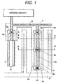
- FIG. 1 is a schematic partial plan view of a lateral insulated gate bipolar transistor in an embodiment of the present invention
- FIG. 2 is a cross sectional view taken along the line A-A' of FIG. 1.
- the numeral mark 1 indicates a semiconductor substrate, which comprises a n conductivity type drift region 3 (first semiconductor region) adjacent to a main surface plane 2; a p conductivity type base region 4 (second semiconductor region) and a p conductivity type collector region 5 (third semiconductor region), which are extending from the main surface plane 2 into the drift region 3, and are provided separately each other, containing a higher impurity concentration than the drift region 3; and a n conductivity type emitter region 6.
- Respective of the base region 4 and the collector region 5 has a stripe structure, and these regions are aligned in a longitudinal direction and provided alternately in a perpendicular direction to the longitudinal direction, as indicated in FIG. 1.
- the emitter region 6 has a stripe shape, and two emitter regions are arranged in the base region 4 in a direction that its longitudinal direction is extending along the longitudinal direction of the base region 4.
- the emitter electrode 7 (first main electrode), expressed by a solid line in FIG.
- the collector electrode 8 (second main electrode) has a comb shape (expressed by a solid line in FIG. 1); its teeth portion 8a is provided along the collector region 5 on the main surface plane 2, and connected electrically to the collector region 5.
- the polycrystalline silicone gate electrode 9, 9a (control electrode) having a stripe structure is arranged above the base region 4, and the drift region 3 and the emitter region 6, respective of which is at adjacent both sides of the base region 4 respectively on the main surface plane 2 via the gate insulating film 10 in a direction that its longitudinal direction is arranged along the longitudinal direction of the base region 4.
- the gate electrode 9 is connected electrically to the adjacent gate electrode 9a at three portions, i.e. the both ends and middle of its longitudinal direction, by the polycrystalline silicone.
- the numerical mark 11 indicates a first insulating film provided on a part of the base region, the gate electrode, and the drift region, as indicated in FIG. 2. Respective of the teeth portion 7a of the emitter electrode 7 and the teeth portion 8a of the collector electrode 8 is extending on the first insulating film 11 to reach on the drift region 3.
- the numerical mark 12 indicates a second insulating film formed above the collector electrode 8, the emitter electrode 7, and the first insulating film 11.
- the gate line 13 having a comb shape is formed on the second insulated film 12 along the emitter electrode 7 with, for instance, aluminum-silicone.
- FIG. 3 indicates a cross sectional view taken along the line B-B' in FIG. 1, that is, the contacting portion of the teeth portion 13a of the gate line 13 with the connecting portion 9b of the gate electrode 9, 9a.
- the connecting portion 9b of the gate electrode 9, 9a is contacting with the gate line 13 by cutting off a part of the emitter electrode 7, the first insulating film 11, and the second insulating film 12 via an aluminum-silicone layer 14.
- the resistance of the gate electrode in the longitudinal direction can be decreased by providing the plural connecting portions 9b of the gate electrode 9, 9a to the gate line 13 along the longitudinal direction of the gate electrode 9, in order to pass the gate current at turn-off condition to the aluminum-silicone line via the nearest connecting point.
- the gate electrodes of the adjacent plural unit IGBT can be readily connected by the gate line 13, and the gate resistance of the whole IGBT can be uniform.
- the operating time at the turn-off operation in the unit IGBT and the operating time of the whole IGBT can be uniform. Therefore, current concentration can be prevented, and consequently, the latch-up preventing performance can be improved.
- the decrease of the gate resistance can be achieved on the main surface plane of the transistor. Therefore, IC can be readily formed, because the IGBT and a driving circuit for driving it can be connected to respective dielectric substrate, SOI substrate, or respective element separated by PN-junction on a same surface plane.
- FIG. 4 is a schematic plan view of the lateral insulated gate bipolar transistor by other one of the embodiments of the present invention.
- the connection points with the gate line are provided at three points, i.e. the both ends and the middle point, of respective of the gate electrodes 9, and 9a, for decreasing the resistance in the longitudinal direction of the gate electrodes 9 and 9a.
- the important point for decreasing the gate resistance in the longitudinal direction is to provide plural connecting points on the polycrystalline silicone gate electrode in the longitudinal direction, and to connect electrically respective of the connecting points with a low resistance line such as aluminum-silicone line.
- FIG. 5 is a schematic plan view of a vertical insulated gate bipolar transistor by an embodiments of the present invention.
- the collector region 5 extends to a portion of the drift region 3 directly under the base and emitter region 4, 6 from the main surface 2. Operation of the respective regions and electrodes are as same as the lateral insulated gate bipolar transistor indicated in FIG. 2. The same advantages as the lateral insulated gate bipolar transistor can be obtained with the vertical insulated gate bipolar transistor.
- the gate resistance of the lateral insulated gate bipolar transistor can be decreased. Accordingly, the operating time at the turn-off operation can be made uniform in the element, and latch-up preventing performance can be improved.
- the present invention can be applied to both lateral and vertical insulated gate transistors such as MOSFET (Metal Oxide Semiconductor Field Effect Transistor).
- MOSFET Metal Oxide Semiconductor Field Effect Transistor
- the collector regions 5 in FIG. 2 and FIG. 5 have n conductivity type, which is opposite to the conductivity type of insulated gate bipolar transistors.
- the gate resistance is decreased, and the turn-off operation is made uniform in the element, Therefore, the current concentration or current crowding is prevented.
- the present invention is applied to an insulated gate transistor in which the p and n conductivity types of the embodiments changes to the n and p conductivity types, namely opposite conductivity types, respectively. In this case, the gate resistance is also reduced.
Landscapes
- Insulated Gate Type Field-Effect Transistor (AREA)
- Bipolar Transistors (AREA)
Abstract
Description
Claims (5)
- An insulated gate transistor comprising:a first semiconductor region of first conductivity type comprising a main surface plane;a second semiconductor region of second conductivity type comprising plural portions provided by extending from said main surface plane into said first semiconductor region,said plural portions, respective of which comprises a stripe shape, are aligned in a longitudinal direction, and provided in parallel;a third semiconductor region;a fourth semiconductor region of the first conductivity type formed along the longitudinal direction of said second semiconductor region, extending from said main surface plane to respective of said plural portions in said second semiconductor region;a first insulation layer formed on said main surface plane crossing over said first, second, and fourth semiconductor regions;control electrodes, which are composed of polycrystalline semiconductor, formed crossing over said first, second, and fourth semiconductor regions via said first insulation layer;a first main electrode connected electrically to said second and fourth semiconductor regions; anda second main electrode connected electrically to said third semiconductor regions on said main surface; whereina metallic wiring layer is provided on said first main surface plane via an insulating layer,plural regions insulated from said first main electrode are provided through said first main electrode, andsaid metallic wiring layer is connected electrically to said control electrode through said insulating layer via said regions insulated from said main electrode.
- An insulated gate transistor as claimed in claim 1, wherein:said plural regions are distributed in the longitudinal direction on the whole surface area of the main electrode.
- An insulated gate transistor as claimed in claim 1, wherein:said insulated gate transistor is a lateral insulated gate bipolar transistor.
- An insulated gate transistor as claimed in claim 1, wherein:said insulated gate transistor is a vertical insulated gate bipolar transistor.
- An integrated circuit comprising:an insulated gate transistor as claimed in any one of claims 1 to 4.
Applications Claiming Priority (2)
| Application Number | Priority Date | Filing Date | Title |
|---|---|---|---|
| JP2696799 | 1999-02-04 | ||
| JP02696799A JP3382172B2 (en) | 1999-02-04 | 1999-02-04 | Horizontal insulated gate bipolar transistor |
Publications (3)
| Publication Number | Publication Date |
|---|---|
| EP1033757A2 true EP1033757A2 (en) | 2000-09-06 |
| EP1033757A3 EP1033757A3 (en) | 2002-03-06 |
| EP1033757B1 EP1033757B1 (en) | 2006-06-21 |
Family
ID=12207938
Family Applications (1)
| Application Number | Title | Priority Date | Filing Date |
|---|---|---|---|
| EP00300577A Expired - Lifetime EP1033757B1 (en) | 1999-02-04 | 2000-01-26 | Insulated gate bipolar transistor |
Country Status (6)
| Country | Link |
|---|---|
| US (1) | US6580108B1 (en) |
| EP (1) | EP1033757B1 (en) |
| JP (1) | JP3382172B2 (en) |
| KR (1) | KR100398532B1 (en) |
| CN (1) | CN1199283C (en) |
| DE (1) | DE60028850T2 (en) |
Families Citing this family (32)
| Publication number | Priority date | Publication date | Assignee | Title |
|---|---|---|---|---|
| EP1265263A4 (en) * | 2000-12-22 | 2006-11-08 | Ngk Insulators Ltd | Electron emission element and field emission display using it |
| US6936972B2 (en) * | 2000-12-22 | 2005-08-30 | Ngk Insulators, Ltd. | Electron-emitting element and field emission display using the same |
| US6946800B2 (en) * | 2002-02-26 | 2005-09-20 | Ngk Insulators, Ltd. | Electron emitter, method of driving electron emitter, display and method of driving display |
| US6897620B1 (en) | 2002-06-24 | 2005-05-24 | Ngk Insulators, Ltd. | Electron emitter, drive circuit of electron emitter and method of driving electron emitter |
| JP3822551B2 (en) * | 2002-09-30 | 2006-09-20 | 日本碍子株式会社 | Light emitting device and field emission display including the same |
| JP2004146364A (en) * | 2002-09-30 | 2004-05-20 | Ngk Insulators Ltd | Light emitting element, and field emission display equipped with it |
| US7067970B2 (en) * | 2002-09-30 | 2006-06-27 | Ngk Insulators, Ltd. | Light emitting device |
| JP2004172087A (en) * | 2002-11-05 | 2004-06-17 | Ngk Insulators Ltd | Display |
| JP2004228065A (en) * | 2002-11-29 | 2004-08-12 | Ngk Insulators Ltd | Electronic pulse emission device |
| JP3867065B2 (en) * | 2002-11-29 | 2007-01-10 | 日本碍子株式会社 | Electron emitting device and light emitting device |
| US7129642B2 (en) * | 2002-11-29 | 2006-10-31 | Ngk Insulators, Ltd. | Electron emitting method of electron emitter |
| US6975074B2 (en) * | 2002-11-29 | 2005-12-13 | Ngk Insulators, Ltd. | Electron emitter comprising emitter section made of dielectric material |
| US7187114B2 (en) * | 2002-11-29 | 2007-03-06 | Ngk Insulators, Ltd. | Electron emitter comprising emitter section made of dielectric material |
| US7379037B2 (en) * | 2003-03-26 | 2008-05-27 | Ngk Insulators, Ltd. | Display apparatus, method of driving display apparatus, electron emitter, method of driving electron emitter, apparatus for driving electron emitter, electron emission apparatus, and method of driving electron emission apparatus |
| US7176609B2 (en) * | 2003-10-03 | 2007-02-13 | Ngk Insulators, Ltd. | High emission low voltage electron emitter |
| US20040189548A1 (en) * | 2003-03-26 | 2004-09-30 | Ngk Insulators, Ltd. | Circuit element, signal processing circuit, control device, display device, method of driving display device, method of driving circuit element, and method of driving control device |
| US7474060B2 (en) * | 2003-08-22 | 2009-01-06 | Ngk Insulators, Ltd. | Light source |
| JP2005070349A (en) * | 2003-08-22 | 2005-03-17 | Ngk Insulators Ltd | Display and its method of driving |
| US7719201B2 (en) * | 2003-10-03 | 2010-05-18 | Ngk Insulators, Ltd. | Microdevice, microdevice array, amplifying circuit, memory device, analog switch, and current control unit |
| US20050116603A1 (en) * | 2003-10-03 | 2005-06-02 | Ngk Insulators, Ltd. | Electron emitter |
| JP2005183361A (en) * | 2003-10-03 | 2005-07-07 | Ngk Insulators Ltd | Electron emitter, electron-emitting device, display, and light source |
| US7336026B2 (en) * | 2003-10-03 | 2008-02-26 | Ngk Insulators, Ltd. | High efficiency dielectric electron emitter |
| JP2005116232A (en) * | 2003-10-03 | 2005-04-28 | Ngk Insulators Ltd | Electron emitting element and its manufacturing method |
| US7190581B1 (en) | 2005-01-11 | 2007-03-13 | Midwest Research Institute | Low thermal resistance power module assembly |
| JP5061443B2 (en) * | 2005-09-20 | 2012-10-31 | 株式会社日立製作所 | Horizontal insulated gate bipolar transistor |
| KR100701159B1 (en) * | 2006-02-01 | 2007-03-28 | 한국전자통신연구원 | Metal-insulator transition element with parallel conducting layer structure |
| JP2008251565A (en) * | 2007-03-29 | 2008-10-16 | Fujitsu Ltd | Semiconductor device |
| US11363951B2 (en) | 2011-09-13 | 2022-06-21 | Glaukos Corporation | Intraocular physiological sensor |
| CN103824858B (en) * | 2012-11-16 | 2016-08-17 | 上海华虹宏力半导体制造有限公司 | The anti-bolt lock structure of CMOS complementary metal-oxide-semiconductor |
| US9730638B2 (en) | 2013-03-13 | 2017-08-15 | Glaukos Corporation | Intraocular physiological sensor |
| JP2018207058A (en) * | 2017-06-09 | 2018-12-27 | ルネサスエレクトロニクス株式会社 | Semiconductor device and method for manufacturing the same |
| US11664436B2 (en) * | 2021-03-01 | 2023-05-30 | Wolfspeed, Inc. | Semiconductor devices having gate resistors with low variation in resistance values |
Family Cites Families (10)
| Publication number | Priority date | Publication date | Assignee | Title |
|---|---|---|---|---|
| JPS57102014A (en) * | 1980-12-17 | 1982-06-24 | Toshiba Corp | Manufacture of semiconductor device |
| JPS6144854A (en) | 1985-06-07 | 1986-03-04 | ソシエテ・デチユ−デ・シヤンテイフイツク・エ・アンデユストリエル・ドウ・リル−ドウ−フランス | N-dichloroalkylbenzoic acid amide and manufacture |
| JP2650519B2 (en) | 1991-07-25 | 1997-09-03 | 株式会社日立製作所 | Horizontal insulated gate transistor |
| DE4402884C1 (en) * | 1994-02-01 | 1995-05-18 | Daimler Benz Ag | Switched power semiconductor element |
| JP3361874B2 (en) * | 1994-02-28 | 2003-01-07 | 三菱電機株式会社 | Field effect type semiconductor device |
| EP0780897B1 (en) * | 1995-12-22 | 2001-03-07 | Consorzio per la Ricerca sulla Microelettronica nel Mezzogiorno | High-speed MOS-technology power device integrated structure with reduced gate resistance |
| KR100194661B1 (en) * | 1995-10-10 | 1999-07-01 | 윤종용 | Power transistor |
| US6140687A (en) * | 1996-11-28 | 2000-10-31 | Matsushita Electric Industrial Co., Ltd. | High frequency ring gate MOSFET |
| JPH10173176A (en) | 1996-12-09 | 1998-06-26 | Toshiba Corp | Semiconductor device |
| JP3545583B2 (en) * | 1996-12-26 | 2004-07-21 | 株式会社ルネサステクノロジ | Semiconductor device and manufacturing method thereof |
-
1999
- 1999-02-04 JP JP02696799A patent/JP3382172B2/en not_active Expired - Fee Related
-
2000
- 2000-01-26 EP EP00300577A patent/EP1033757B1/en not_active Expired - Lifetime
- 2000-01-26 DE DE60028850T patent/DE60028850T2/en not_active Expired - Fee Related
- 2000-02-01 KR KR10-2000-0004853A patent/KR100398532B1/en not_active Expired - Fee Related
- 2000-02-03 US US09/497,213 patent/US6580108B1/en not_active Expired - Fee Related
- 2000-02-04 CN CNB001019988A patent/CN1199283C/en not_active Expired - Fee Related
Also Published As
| Publication number | Publication date |
|---|---|
| KR100398532B1 (en) | 2003-09-19 |
| JP3382172B2 (en) | 2003-03-04 |
| CN1263360A (en) | 2000-08-16 |
| US6580108B1 (en) | 2003-06-17 |
| EP1033757B1 (en) | 2006-06-21 |
| KR20000057854A (en) | 2000-09-25 |
| DE60028850D1 (en) | 2006-08-03 |
| JP2000223707A (en) | 2000-08-11 |
| CN1199283C (en) | 2005-04-27 |
| DE60028850T2 (en) | 2007-06-28 |
| EP1033757A3 (en) | 2002-03-06 |
Similar Documents
| Publication | Publication Date | Title |
|---|---|---|
| EP1033757B1 (en) | Insulated gate bipolar transistor | |
| JP7529750B2 (en) | Semiconductor device and power module | |
| US7598566B2 (en) | Trench gate field effect devices | |
| KR100745557B1 (en) | ITV and power converter | |
| JP4310017B2 (en) | Semiconductor device and power conversion device | |
| US7893457B2 (en) | Bipolar mosfet devices and methods for their use | |
| EP2342753B1 (en) | Insulated gate bipolar transistor | |
| US6133607A (en) | Semiconductor device | |
| EP0697739B1 (en) | Insulated gate bipolar transistor | |
| US20150228744A1 (en) | Transistor device with integrated gate-resistor | |
| US11810912B2 (en) | Semiconductor devices having asymmetric integrated gate resistors for balanced turn-on/turn-off behavior | |
| EP0526037B1 (en) | Lateral insulated gate bipolar transistor and corresponding array | |
| US20060081919A1 (en) | Semiconductor device | |
| US11158627B2 (en) | Electronic circuit with a transistor device and a clamping circuit | |
| US5440164A (en) | MOS/bipolar device | |
| KR100316723B1 (en) | Power MOSFET having low on-resistance and high ruggedness | |
| JP2005150348A (en) | Semiconductor device | |
| JP2004363477A (en) | Insulated gate semiconductor device | |
| JP4829003B2 (en) | Semiconductor device and power conversion device | |
| US20240250678A1 (en) | Electronic circuit with a transistor device and a protection circuit | |
| US20220262898A1 (en) | Igbt light load efficiency | |
| JPH1140818A (en) | Semiconductor device | |
| EP0650195B1 (en) | MOS/bipolar device |
Legal Events
| Date | Code | Title | Description |
|---|---|---|---|
| PUAI | Public reference made under article 153(3) epc to a published international application that has entered the european phase |
Free format text: ORIGINAL CODE: 0009012 |
|
| 17P | Request for examination filed |
Effective date: 20000215 |
|
| AK | Designated contracting states |
Kind code of ref document: A2 Designated state(s): AT BE CH CY DE DK ES FI FR GB GR IE IT LI LU MC NL PT SE Kind code of ref document: A2 Designated state(s): DE GB |
|
| AX | Request for extension of the european patent |
Free format text: AL;LT;LV;MK;RO;SI |
|
| PUAL | Search report despatched |
Free format text: ORIGINAL CODE: 0009013 |
|
| AK | Designated contracting states |
Kind code of ref document: A3 Designated state(s): AT BE CH CY DE DK ES FI FR GB GR IE IT LI LU MC NL PT SE |
|
| AX | Request for extension of the european patent |
Free format text: AL;LT;LV;MK;RO;SI |
|
| AKX | Designation fees paid |
Free format text: DE GB |
|
| GRAP | Despatch of communication of intention to grant a patent |
Free format text: ORIGINAL CODE: EPIDOSNIGR1 |
|
| GRAS | Grant fee paid |
Free format text: ORIGINAL CODE: EPIDOSNIGR3 |
|
| GRAA | (expected) grant |
Free format text: ORIGINAL CODE: 0009210 |
|
| AK | Designated contracting states |
Kind code of ref document: B1 Designated state(s): DE GB |
|
| REG | Reference to a national code |
Ref country code: GB Ref legal event code: FG4D |
|
| REF | Corresponds to: |
Ref document number: 60028850 Country of ref document: DE Date of ref document: 20060803 Kind code of ref document: P |
|
| PLBE | No opposition filed within time limit |
Free format text: ORIGINAL CODE: 0009261 |
|
| STAA | Information on the status of an ep patent application or granted ep patent |
Free format text: STATUS: NO OPPOSITION FILED WITHIN TIME LIMIT |
|
| 26N | No opposition filed |
Effective date: 20070322 |
|
| PGFP | Annual fee paid to national office [announced via postgrant information from national office to epo] |
Ref country code: DE Payment date: 20090219 Year of fee payment: 10 |
|
| PGFP | Annual fee paid to national office [announced via postgrant information from national office to epo] |
Ref country code: GB Payment date: 20081229 Year of fee payment: 10 |
|
| GBPC | Gb: european patent ceased through non-payment of renewal fee |
Effective date: 20100126 |
|
| PG25 | Lapsed in a contracting state [announced via postgrant information from national office to epo] |
Ref country code: DE Free format text: LAPSE BECAUSE OF NON-PAYMENT OF DUE FEES Effective date: 20100803 |
|
| PG25 | Lapsed in a contracting state [announced via postgrant information from national office to epo] |
Ref country code: GB Free format text: LAPSE BECAUSE OF NON-PAYMENT OF DUE FEES Effective date: 20100126 |