EP1032856B1 - Optisches sende/empfangsmodul - Google Patents
Optisches sende/empfangsmodul Download PDFInfo
- Publication number
- EP1032856B1 EP1032856B1 EP98961112A EP98961112A EP1032856B1 EP 1032856 B1 EP1032856 B1 EP 1032856B1 EP 98961112 A EP98961112 A EP 98961112A EP 98961112 A EP98961112 A EP 98961112A EP 1032856 B1 EP1032856 B1 EP 1032856B1
- Authority
- EP
- European Patent Office
- Prior art keywords
- optical
- coupling
- transmitter
- receiver
- mirror
- Prior art date
- Legal status (The legal status is an assumption and is not a legal conclusion. Google has not performed a legal analysis and makes no representation as to the accuracy of the status listed.)
- Expired - Lifetime
Links
- 230000003287 optical effect Effects 0.000 title claims description 38
- 239000000835 fiber Substances 0.000 claims description 43
- 238000005516 engineering process Methods 0.000 claims description 28
- 238000010168 coupling process Methods 0.000 claims description 25
- 238000005859 coupling reaction Methods 0.000 claims description 25
- 230000008878 coupling Effects 0.000 claims description 19
- 239000002184 metal Substances 0.000 claims description 5
- 229910052751 metal Inorganic materials 0.000 claims description 5
- 239000011521 glass Substances 0.000 claims description 2
- 229920000642 polymer Polymers 0.000 claims description 2
- 239000004020 conductor Substances 0.000 claims 2
- 230000005540 biological transmission Effects 0.000 description 13
- 238000004049 embossing Methods 0.000 description 11
- 238000000034 method Methods 0.000 description 11
- 239000000463 material Substances 0.000 description 5
- 239000013307 optical fiber Substances 0.000 description 5
- PCHJSUWPFVWCPO-UHFFFAOYSA-N gold Chemical compound [Au] PCHJSUWPFVWCPO-UHFFFAOYSA-N 0.000 description 3
- 239000010931 gold Substances 0.000 description 3
- 229910052737 gold Inorganic materials 0.000 description 3
- 229910052710 silicon Inorganic materials 0.000 description 3
- 239000010703 silicon Substances 0.000 description 3
- 238000011161 development Methods 0.000 description 2
- 230000018109 developmental process Effects 0.000 description 2
- 238000012545 processing Methods 0.000 description 2
- 230000008054 signal transmission Effects 0.000 description 2
- RYGMFSIKBFXOCR-UHFFFAOYSA-N Copper Chemical compound [Cu] RYGMFSIKBFXOCR-UHFFFAOYSA-N 0.000 description 1
- 239000000853 adhesive Substances 0.000 description 1
- 230000001070 adhesive effect Effects 0.000 description 1
- 239000012876 carrier material Substances 0.000 description 1
- 239000011248 coating agent Substances 0.000 description 1
- 238000000576 coating method Methods 0.000 description 1
- 229910052802 copper Inorganic materials 0.000 description 1
- 239000010949 copper Substances 0.000 description 1
- 238000013461 design Methods 0.000 description 1
- 239000004744 fabric Substances 0.000 description 1
- 239000003365 glass fiber Substances 0.000 description 1
- 230000036039 immunity Effects 0.000 description 1
- 238000003780 insertion Methods 0.000 description 1
- 230000037431 insertion Effects 0.000 description 1
- 238000004519 manufacturing process Methods 0.000 description 1
- 238000005457 optimization Methods 0.000 description 1
- 238000004806 packaging method and process Methods 0.000 description 1
- 239000004065 semiconductor Substances 0.000 description 1
- 239000012780 transparent material Substances 0.000 description 1
Images

Classifications
-
- G—PHYSICS
- G02—OPTICS
- G02B—OPTICAL ELEMENTS, SYSTEMS OR APPARATUS
- G02B6/00—Light guides; Structural details of arrangements comprising light guides and other optical elements, e.g. couplings
- G02B6/24—Coupling light guides
- G02B6/42—Coupling light guides with opto-electronic elements
- G02B6/4201—Packages, e.g. shape, construction, internal or external details
- G02B6/4246—Bidirectionally operating package structures
-
- G—PHYSICS
- G02—OPTICS
- G02B—OPTICAL ELEMENTS, SYSTEMS OR APPARATUS
- G02B6/00—Light guides; Structural details of arrangements comprising light guides and other optical elements, e.g. couplings
- G02B6/24—Coupling light guides
- G02B6/42—Coupling light guides with opto-electronic elements
- G02B6/4201—Packages, e.g. shape, construction, internal or external details
- G02B6/4204—Packages, e.g. shape, construction, internal or external details the coupling comprising intermediate optical elements, e.g. lenses, holograms
- G02B6/4214—Packages, e.g. shape, construction, internal or external details the coupling comprising intermediate optical elements, e.g. lenses, holograms the intermediate optical element having redirecting reflective means, e.g. mirrors, prisms for deflecting the radiation from horizontal to down- or upward direction toward a device
Definitions
- the invention relates to an optical transmitter / receiver module according to the preamble of Claim 1 or 2.
- Optical fibers such as Glass fibers or plastic fiber optic cables.
- optical data buses In optical data buses, however, Compared to electrical data buses always additional optical transmission and Receiving modules as electrical / optical or optical / electrical converters required because the Signal processing in the bus participants is still done electrically. This will additional costs and volume and weight.
- both two optical fibers (so-called two-wire technology) and one Optical fiber (so-called Single wire technology)
- the advantage of single wire technology is that a minimum number of Lines and connectors are used in the physical bus layer, whereby however, additional coupling elements such as, for example, in the optical transceiver module Y couplers must be integrated, which cause additional transmission losses.
- a carrier module for one transmit and one Receiving element contains a carrier body made of optically transparent material.
- the end section of an optical waveguide is inserted in the groove of the carrier body.
- the groove ends in a partially permeable sloping surface that serves as a send / receive switch.
- Optical fiber incoming light is through the partially transparent mirror surface through the Material of the carrier body passed to a receiving element. From a sending element emitted light is deflected into the optical waveguide on the mirror surface. Since the support body must be partially transparent on the deflecting mirror surface, the Material selection limited to transparent fabrics.
- total coupling efficiency as a product of coupling and decoupling efficiency less than 25%.
- both a transmission module is known from the document WO 97 36201 A, in which means a mirrored, opaque carrier plate, light is diverted from a transmitter into a transmission fiber becomes light from a receiving fiber to a receiver as well as by means of a carrier plate leads.
- the invention is therefore based on the object of an optical transmitter / receiver module to indicate that an optimized arrangement for Increased efficiency in signal processing and characterized by a compact design as well as simple and therefore inexpensive with a wide range of materials designed.
- the optical transmitter / receiver module consists of a carrier plate, a transmitter, a receiver, optical fiber (s) and can be used for two-wire technology or single-wire technology with an additional Y-coupling element or single-wire technology without an additional Y-coupling element.
- the basic element of this arrangement is a metal or plastic carrier plate, which is coated with a reflective coating and is thus opaque and into which embossing technology, for example V-shaped or U-shaped or rectangular grooves, for receiving multimode waveguides, deflecting mirrors with adjustable inclination, area and surface quality for deflecting the light to be coupled in and out and recesses for receiving the transmitter or receiver are embossed.
- embossing technology for example V-shaped or U-shaped or rectangular grooves
- a gold layer can be used as the opaque reflecting layer on the carrier plate.
- a surface emitting laser diode with a vertical resonator (VCSEL; vertical cavity surface emitting laser) is particularly suitable as an optical transmitter in conjunction with a photodiode as a receiver.
- the transmit / receive fibers consist of cylindrical multimode light waveguides made of glass or polymers with a core diameter of at least 50 ⁇ m.
- two separate ones on the carrier plate reflecting into the reflecting technique coated surface, grooves for receiving the transmitting and receiving fibers and two separate coupling and decoupling mirrors and the optical transmitter and receiver attached directly above the mirrors in pre-embossed recesses.
- a groove made by means of embossing technology in the mirror-coated surface for receiving the transmitting / receiving fiber in addition to this a coupling mirror that only partially shades the fiber end, and in a further extension a coupling mirror that does this
- the end of the fiber is completely shaded, embossed and the optical transmitter and receiver are attached directly above the mirrors in pre-embossed recesses.
- the optical transmitter is arranged in a pre-embossed recess directly above it, and in a further extension to the fiber, the optical receiver is arranged directly behind the coupling mirror in pre-embossed recesses.
- the embossing technique used can also be used if housed transmitters and receivers are used instead of VCSEL and photodiode chips. A combination of housed and non-housed components is also possible.
- a major advantage of the invention and particularly rational is that Use of the embossing technique, with the desired structure using an embossing stamp is stamped into the surface of the carrier plate, an inexpensive, compact Structure is achieved.
- Another significant advantage of the invention is that, for example Coupling elements with low insertion losses in the embossed carrier plate of the module can be integrated, so that compact, low-loss transmit / receive modules for Single-wire data buses are available.
- transmitter and receiver can be added to additional Y-coupling elements be dispensed with by the coupling mirror only a certain part of the light shadows that emerges from the transmit / receive fiber.
- the unshaded portion is coupled to the detector.
- the proposed embossing technique makes it possible the height and angle of the coupling mirror with regard to maximum Coupling the light of a given transmitter into a given fiber optimize. Through optimization, overall efficiencies can be significantly higher than 25% can be achieved.
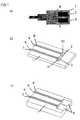
- the transmission / reception module shown schematically in Fig. 1a consists of a carrier plate 1, an optical transmitter 2, an optical receiver 3 and a transmission fiber 4 and a reception fiber 5, both of which open into a guide sleeve (two-wire technology).
- V-shaped grooves 6 and 7, for example, for receiving the transmission and reception fibers 4 and 5 are embossed into the carrier plate 1 (FIG. 1b) by means of embossing technology.
- receptacles for the optical transmitter 2 and receiver 3 and the inclined surface of the coupling and decoupling mirrors 10, 11 are formed at the end of the V-shaped longitudinal grooves.
- Transmitter 2 and receiver 3 are inserted into the receptacles using flip-chip technology and are located directly above the coupling and decoupling mirrors 10, 11.
- the carrier plate 1 made of metal and / or plastic is covered by an opaque, reflective metal layer, which consists, for example, of gold or, for reasons of adhesive strength on materials with different thermal expansion, of a multilayer structure such as copper / gold.
- the metal layer can be applied either before the embossing process or subsequently, if necessary also only in the region of the V-shaped grooves 6, 7 and the coupling and decoupling mirrors 10, 11.
- the arrangement of the fibers 4, 5, the deflecting mirrors 10, 11, the transmitter 2 and the receiver 3 are positioned precisely in the beam path, so that the light emitted in the transmitter 2 reflects on the opaque coupling mirror 10 and, depending on the mode selection, at a defined angle, is fed into the transmission fiber 4; or the light guided in the receiving fiber 5 is reflected by the opaque coupling mirror 11 and is detected in the receiver 3 positioned in the beam path.
- Deflecting mirrors can also be dispensed with as soon as, for example, transmitter 2 and receiver 3 are used in TO housings, which are used in receptacles 8 provided for this in a linear continuation to the fiber axes (FIG. 1c).
- the transmission mirror 10 has at least one height that closes off the fiber 4 at the top, in order to completely transmit a light beam that is fed into the transmission fiber along the fiber axis, in particular when the mirror surface is inclined by 45 °. As shown in FIG.
- the mirror height and inclination can be variably selected depending on the entry angle in a range predetermined by the ray path.
- This procedure forms the basis of an arrangement of fiber, transmitter and receiver one behind the other in a plane running along the fiber axis and perpendicular to the carrier plate.
- the arrangement now contains only a combined transmit / receive fiber, and an additional Y-coupling element can be dispensed with.
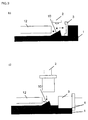
- FIG. 3 a shows the coupling-out mirror 10 arranged below the transmitter 2, which only shades a certain part of the light that strikes the coupling-out mirror 11 from the transmit / receive fiber 12 in order to be registered in the detector 3.
- the decoupling mirror is inclined as flat as possible, a considerable gain in the intensity of the signal to be evaluated can be achieved in the detector.
- a further increase is to be expected from the arrangement shown in FIG. 3b, in which a coupling-out mirror can be dispensed with entirely, in that the detector 3 is mounted directly in the beam path of the signal emerging from the transmission / reception fiber and thus certain intensity losses when deflecting are avoided .
- housed components can also be integrated into the arrangement.
- the receptacle 8 for a TO housing can be produced simply and precisely using embossing technology.
Landscapes
- Physics & Mathematics (AREA)
- General Physics & Mathematics (AREA)
- Optics & Photonics (AREA)
- Optical Couplings Of Light Guides (AREA)
Description
Als optische Sender eignet sich besonders eine oberflächenemittierende Laserdiode mit Vertikalresonator (VCSEL; vertical cavity surface emitting laser) in Verbindung mit einer Photodiode als Empfänger. Die Sende-/Empfangsfasern bestehen aus zylindrischen Mehrmodenlichtwellenleitern aus Glas oder Polymeren mit Kerndurchmesser von mindestens 50µm.
Desweiteren sind im Falle der Einleitertechnik ohne zusätzliches Koppelelement auf der Trägerplatte eine mittels Prägetechnik in die spiegelnd beschichtete Oberfläche eingebrachte Nut zur Aufnahme der Sende/Empfangsfaser, in Verlängerung dazu ein Einkoppelspiegel, der das Faserende nur teilweise abschattet, in weiterer Verlängerung ein Auskoppelspiegel, der das Faserende vollständig abschattet, eingeprägt und der optische Sender und Empfänger direkt über den Spiegeln in vorgeprägten Vertiefungen angebracht.
Alternativ hierzu sind der optische Sender in einer vorgeprägten Vertiefung direkt darüber angeordnet und in weiterer Verlängerung zur Faser der optische Empfänger direkt hinter dem Einkoppelspiegel in vorgeprägten Vertiefungen angebracht.
Die verwendete Prägetechnik kann auch dann angewandt werden, wenn statt VCSEL- und Photodiodenchips gehäuste Sender und Empfänger Verwendung finden. Auch eine Kombination aus gehäusten und nichtgehäusten Bauelementen ist möglich.
- Fig. 1a
- Sende/Empfangsmodul in Zweileitertechnik;
- Fig. 1b
- Detailansicht des Sende/Empfangsmodul mit Umlenkspiegeln;
- Fig. 1c
- Detailansicht des Sende/Empfangsmodul ohne Umlenkspiegeln;
- Fig. 2a
- Sende/Empfangsmodul in Einleitertechnik mit Y-Koppler;
- Fig. 2b
- Querschnitt des Sendemoduls mit Umlenkspiegel;
- Fig. 3a
- Detailansicht des Sende/Empfangsmodul in Einleitertechnik ohne Koppler mit zwei Umlenkspiegeln;
- Fig. 3b
- Querschnitt des Sende/Empfangsmodul in Einleitertechnik ohne Koppler mit einem Umlenkspiegel für den Sender;
- Fig. 3c
- Querschnitt des Sende/Empfangsmodul in Einleitertechnik ohne Koppler mit einem Umlenkspiegel für den Sender in gehäuster Ausführung.
In die Trägerplatte 1 (Fig.1b) sind mittels Prägetechnik beispielsweise V-förmige Nuten 6 und 7 zur Aufnahme der Sende- und Empfangsfasern 4 und 5 eingeprägt. Ebenfalls mittels Prägetechnik sind Aufnahmen für den optischen Sender 2 und Empfänger 3 und die Schrägfläche der Ein- bzw. Auskoppelspiegel 10, 11 am Ende der V-förmigen Längsnuten geformt. Sender 2 und Empfänger 3 sind dabei in flip-chip Technik in die Aufnahmen eingefügt und befinden sich jeweils unmittelbar über dem Ein- bzw. Auskoppelspiegel 10, 11. Die Trägerplatte 1 aus Metall und/oder Kunststoff wird von einer opaken, spiegelnden Metallschicht bedeckt, die beispielsweise aus Gold oder, aus Gründen der Haftfestigkeit auf Materialien unterschiedlicher Wärmeausdehnung, aus einer Mehrlagenstruktur wie beispielsweise Kupfer/Gold besteht. Dabei kann die Metallschicht entweder vor dem Prägevorgang oder nachträglich, gegebenenfalls auch nur im Bereich der V-förmigen Nuten 6, 7 und dem Ein- bzw. Auskoppelspiegel 10, 11 aufgebracht werden.
Die Anordnung der Fasern 4, 5, der Umlenkspiegel 10, 11, der Sender 2 und Empfänger 3 sind präzise im Strahlweg positioniert, so daß das im Sender 2 ausgesandte Licht am opaken Auskoppelspiegel 10 reflektiert und in Abhängigkeit von der Modenauswahl unter einem definierten Winkel, in die Sendefaser 4 eingespeist wird; bzw. das in der Empfangsfaser 5 geführte Licht über den opaken Einkoppelspiegel 11 reflektiert und in dem im Strahlengang positionierten Empfänger 3 detekiert wird.
Auf Umlenkspiegel kann auch verzichtet werden, sobald beispielsweise Sender 2 und Empfänger 3 in TO-Gehäuse verwendet werden, die in dafür vorgesehene Aufnahmen 8 in linearer Fortsetzung zu den Faserachsen eingesetzt werden (Fig. 1c).
Das in Fig.2a schematisch dargestellte Sende/Empfangsmodul besteht ebenfalls aus einer Trägerplatte 1, einem optischen Sender 2, einem optischen Empfänger 3 sowie einer Sendefaser 4 und einer Empfangsfaser 5, die jedoch über einen Y-Koppler 9 auf der Trägerplatte 1 zusammengeführt wird, so daß im weiteren Verlauf nur noch eine Faser in die Führungshülse einmündet (Einleitertechnik).
Bei beiden beschriebenen Einleiter/Zweileiter-Techniken besitzt der Sendespiegel 10 zumindest eine mit der Oberseite die Faser 4 abschließende Höhe, um bei einer Neigung der Spiegelfläche von 45° insbesondere einen entlang der Faserachse in die Sendefaser eingespeisten Lichtstrahl vollständig zu übertragen.
Wie in Fig. 2b für die Sendeeinheit dargestellt, kann für außerhalb der Faserachse eingespeiste Lichtstrahlen, die Spiegelhöhe und Neigung in Abhängigkeit vom Eintrittswinkel in einem vom Strahlenverlauf vorgegebenen Bereich variabel gewählt werden.
Diese Vorgehensweise bildet die Basis einer Anordnung von Faser, Sender und Empfänger hintereinander in einer entlang der Faserachse verlaufenden und zur Trägerplatte senkrecht stehenden Ebene. Die Anordnung enthält nur noch eine kombinierte Sende/Empfangsfaser, wobei auf ein zusätzliches Y-Koppelelement verzichtet werden kann. Einige Ausführungsformen sind in Fig. 3 dargestellt. Der Querschnitt in Fig. 3a zeigt den unterhalb des Senders 2 angeordneten Auskoppelspiegel 10, der lediglich einen gewissen Teil des Lichts abschattet, das aus der Sende/Empfangs-Faser 12 auf den Auskoppelspiegel 11 trifft, um im Detektor 3 registiert zu werden. Bei möglichst flacher Neigung des Auskoppelspiegels kann dadurch ein beträchtlicher Intensitätsgewinn des auszuwertenden Signals im Detektor erzielt werden. Eine weitere Steigerung ist von der in Fig. 3b dargestellten Anordnung zu erwarten, bei der auf einen Auskoppelspiegel ganz verzichtet werden kann, indem der Detektor 3 direkt im Strahlengang des aus der Sende/Empfangsfaser austretenden Signals angebracht ist und damit gewisse Intensitätsverluste beim Umlenken vermieden werden. In gleicher Weise können auch gehäuste Bauteile in die Anordnung integriert werden. Die Aufnahme 8 für ein TO-Gehäuse ist wie in allen vorherigen Beispielen mittels Prägetechnik einfach und präzise herstellbar.
Claims (5)
- Optisches Sende/Empfangsmodul insbesondere für Einleitertechnik, bestehend aus einer spiegelnd beschichteten, opaken Trägerplatte (1), optischen Sende-/Empfangsfaser(n) (12), einem Sender (2) als Laserdiode und einem Empfänger (3), dadurch gekennzeichnet,dass auf der Trägerplatte (1) eine in die spiegelnd beschichtete Oberfläche eingebrachte Nut in der die Sende/Empfangsfaser (12) angeordnet ist,dass in Verlängerung der Nut ein Einkoppelspiegel (10) eingeprägt ist, der das Faserende nur teilweise abschattet und dessen Neigung in Abhängigkeit von der Modenauswahl unter einem definierten Winkel zur maximalen Einkopplung des Lichts festgelegt ist,dass in weiterer Verlängerung der Nut ein Auskoppelspiegel (11) eingeprägt ist, der das Faserende vollständig abschattet, unddass der optische Sender (2) und Empfänger (3) direkt über den Spiegeln angebracht sind (Fig 3a).
- Optisches Sende/Empfangsmodul insbesondere für Einleitertechnik, bestehend aus einer spiegelnd beschichteten, opaken Trägerplatte (1), optischen Sende-/Empfangsfaser(n) (12), einem Sender (2) als Laserdiode und einem Empfänger (3), dadurch gekennzeichnet,dass auf der Trägerplatte (1) eine in die spiegelnd beschichtete Oberfläche eingebrachte Nut in der die Sende/Empfangsfaser (12) angeordnet ist,dass in Verlängerung der Nut ein Einkoppelspiegel (10) eingeprägt ist, der das Faserende nur teilweise abschattet und dessen Neigung in Abhängigkeit von der Modenauswahl unter einem definierten Winkel zur maximalen Einkopplung des Lichts festgelegt ist,dass ein optischer Sender (2) direkt über dem Einkoppelspiegel (10) angeordnet ist, unddass in weiterer Verlängerung zur Faser (12) ein optischer Empfänger (3) direkt hinter dem Einkoppelspiegel (10) angebracht ist (Fig. 3b).
- Optisches Sende/Empfangsmodul nach Anspruch 1 oder 2, dadurch gekennzeichnet, daf die Trägerplatte aus Metall oder Kunststoff besteht.
- Optisches Sende/Empfangsmodul nach einem der Ansprüche 1 bis 3, dadurch gekennzeichnet, daß die optischen Sende-/Empfangsfaser(n) aus zylindrischen Mehrmodenlichtwellenleitern aus Glas oder Polymeren mit Kerndurchmesser von mindestens 50µm bestehen.
- Optisches Sende/Empfangsmodul nach einem der vorhergehende Ansprüche, dadurch gekennzeichnet, daß der optische Sender (2) und/oder Empfänger (3) gehäust vorliegen (3c).
Applications Claiming Priority (3)
| Application Number | Priority Date | Filing Date | Title |
|---|---|---|---|
| DE19748989A DE19748989A1 (de) | 1997-11-06 | 1997-11-06 | Optisches Sende/Empfangsmodul |
| DE19748989 | 1997-11-06 | ||
| PCT/EP1998/006883 WO1999024855A1 (de) | 1997-11-06 | 1998-10-30 | Optisches sende/empfangsmodul |
Publications (2)
| Publication Number | Publication Date |
|---|---|
| EP1032856A1 EP1032856A1 (de) | 2000-09-06 |
| EP1032856B1 true EP1032856B1 (de) | 2001-12-12 |
Family
ID=7847761
Family Applications (1)
| Application Number | Title | Priority Date | Filing Date |
|---|---|---|---|
| EP98961112A Expired - Lifetime EP1032856B1 (de) | 1997-11-06 | 1998-10-30 | Optisches sende/empfangsmodul |
Country Status (4)
| Country | Link |
|---|---|
| US (1) | US6402394B1 (de) |
| EP (1) | EP1032856B1 (de) |
| DE (2) | DE19748989A1 (de) |
| WO (1) | WO1999024855A1 (de) |
Families Citing this family (15)
| Publication number | Priority date | Publication date | Assignee | Title |
|---|---|---|---|---|
| DE19932430C2 (de) * | 1999-07-12 | 2002-03-14 | Harting Elektrooptische Bauteile Gmbh & Co Kg | Opto-elektronische Baugruppe sowie Bauteil für diese Baugruppe |
| KR100476314B1 (ko) * | 2002-10-25 | 2005-03-15 | 한국전자통신연구원 | 실리콘 광벤치를 이용한 광송신 모듈 |
| US20160274318A1 (en) * | 2012-03-05 | 2016-09-22 | Nanoprecision Products, Inc. | Optical bench subassembly having integrated photonic device |
| US9782814B2 (en) * | 2012-03-05 | 2017-10-10 | Nanoprecision Products, Inc. | Stamping to form a composite structure of dissimilar materials having structured features |
| JP6273217B2 (ja) * | 2012-03-05 | 2018-01-31 | ナノプレシジョン プロダクツ インコーポレイテッドNanoprecision Products, Inc. | 光ファイバの入力/出力を結合するための構造化反射表面を有する結合装置 |
| US20130294732A1 (en) | 2012-03-05 | 2013-11-07 | Nanoprecision Products, Inc. | Hermetic optical fiber alignment assembly having integrated optical element |
| US20150355420A1 (en) * | 2012-03-05 | 2015-12-10 | Nanoprecision Products, Inc. | Coupling device having a stamped structured surface for routing optical data signals |
| US20160377821A1 (en) * | 2012-03-05 | 2016-12-29 | Nanoprecision Products, Inc. | Optical connection of optical fibers to grating couplers |
| JP6683627B2 (ja) * | 2014-05-15 | 2020-04-22 | ナノプレシジョン プロダクツ インコーポレイテッドNanoprecision Products, Inc. | グレーディングカプラへの光ファイバの光接続 |
| MX377726B (es) * | 2014-05-15 | 2025-03-11 | Nanoprecision Products Inc | Estampado para formar una estructura compuesta de materiales disimilares que tienen elementos estructurados. |
| KR20170129236A (ko) * | 2015-03-22 | 2017-11-24 | 나노프리시젼 프로덕츠 인코포레이션 | 통합된 광 장치를 가지는 광학적 벤치 하위조립체 |
| US9864145B2 (en) | 2015-08-12 | 2018-01-09 | Nanoprecision Products, Inc. | Multiplexer/demultiplexer using stamped optical bench with micro mirrors |
| CN109424562B (zh) * | 2017-08-25 | 2020-08-07 | 技嘉科技股份有限公司 | 混合反光及导光机制的发光风扇装置 |
| TWI638947B (zh) * | 2017-08-25 | 2018-10-21 | 技嘉科技股份有限公司 | 混合反光及導光機制的發光風扇裝置 |
| US12345923B2 (en) | 2021-10-20 | 2025-07-01 | Senko Advanced Components, Inc. | Metallized optical fiber array module and fabrication method thereof |
Family Cites Families (23)
| Publication number | Priority date | Publication date | Assignee | Title |
|---|---|---|---|---|
| JPS5967678A (ja) * | 1982-10-12 | 1984-04-17 | Hitachi Ltd | 光フアイバ−付レ−ザ−ダイオ−ド装置 |
| US4611884A (en) * | 1982-11-24 | 1986-09-16 | Magnetic Controls Company | Bi-directional optical fiber coupler |
| CA1255382A (en) * | 1984-08-10 | 1989-06-06 | Masao Kawachi | Hybrid optical integrated circuit with alignment guides |
| US4904036A (en) * | 1988-03-03 | 1990-02-27 | American Telephone And Telegraph Company, At&T Bell Laboratories | Subassemblies for optoelectronic hybrid integrated circuits |
| WO1990002349A1 (en) | 1988-08-31 | 1990-03-08 | Raynet Corporation | Method of deforming a polymer optical fiber to form taps |
| DE4013630A1 (de) * | 1989-05-31 | 1990-12-06 | Siemens Ag | Optoelektronischer wandlermodul und verfahren zu dessen herstellung |
| DE4005141A1 (de) * | 1990-02-17 | 1991-09-05 | Stribel Gmbh | Optoelektronische einrichtung |
| DE9010135U1 (de) * | 1990-07-04 | 1990-09-06 | Siemens AG, 8000 München | Empfangsgerät für optische Signale |
| DE4101962A1 (de) * | 1991-01-24 | 1992-07-30 | Telefunken Systemtechnik | Anordnung zur uebertragung von daten mit mindestens einem lichtwellenleiter |
| SE468150B (sv) * | 1991-05-06 | 1992-11-09 | Asea Brown Boveri | Optoelektronisk komponent |
| US5201018A (en) | 1991-08-29 | 1993-04-06 | Codenoll Technology Corporation | Optical connector with waveguides for device to fiber coupling |
| DE4212208A1 (de) * | 1992-04-10 | 1993-10-14 | Bosch Gmbh Robert | Verfahren zur Herstellung optischer Polymerbauelemente mit integrierter Faser-Chip-Kopplung in Abformtechnik |
| DE4230952A1 (de) * | 1992-09-16 | 1994-03-17 | Sel Alcatel Ag | Optischer Duplexer |
| DE4402166B4 (de) * | 1993-05-04 | 2005-04-21 | Daimlerchrysler Ag | Endstellenmodul für bidirektionale optische Signalübertragung und Verfahren zu dessen Herstellung |
| US5359447A (en) * | 1993-06-25 | 1994-10-25 | Hewlett-Packard Company | Optical communication with vertical-cavity surface-emitting laser operating in multiple transverse modes |
| US5487124A (en) * | 1994-06-30 | 1996-01-23 | The Whitaker Corporation | Bidirectional wavelength division multiplex transceiver module |
| DE19501285C1 (de) * | 1995-01-18 | 1996-05-15 | Bosch Gmbh Robert | Anordnung zur Umsetzung von optischen in elektrische Signale und Verfahren zur Herstellung |
| DE19523267A1 (de) * | 1995-06-27 | 1997-01-02 | Bosch Gmbh Robert | Lasermodul |
| SE510049C2 (sv) * | 1996-03-25 | 1999-04-12 | Ericsson Telefon Ab L M | Anordning för att ansluta minst en vågledare till en optisk sändare eller mottagare |
| DE19616015C1 (de) * | 1996-04-23 | 1997-06-19 | Bosch Gmbh Robert | Anordnung zur Ankopplung optischer Sende- oder Empfangselemente an einen Lichtwellenleiter |
| DE19616932A1 (de) * | 1996-04-27 | 1997-10-30 | Bosch Gmbh Robert | Optisches, strahlteilendes Bauelement sowie Verfahren zur Herstellung einer Prismenträgerplatte für ein solches Bauelement |
| JP3191729B2 (ja) * | 1997-07-03 | 2001-07-23 | 日本電気株式会社 | 光半導体モジュールとその製造方法 |
| JP3792040B2 (ja) * | 1998-03-06 | 2006-06-28 | 松下電器産業株式会社 | 双方向光半導体装置 |
-
1997
- 1997-11-06 DE DE19748989A patent/DE19748989A1/de not_active Withdrawn
-
1998
- 1998-10-30 WO PCT/EP1998/006883 patent/WO1999024855A1/de not_active Ceased
- 1998-10-30 EP EP98961112A patent/EP1032856B1/de not_active Expired - Lifetime
- 1998-10-30 US US09/530,980 patent/US6402394B1/en not_active Expired - Lifetime
- 1998-10-30 DE DE59802474T patent/DE59802474D1/de not_active Expired - Lifetime
Also Published As
| Publication number | Publication date |
|---|---|
| DE59802474D1 (de) | 2002-01-24 |
| DE19748989A1 (de) | 1999-07-15 |
| WO1999024855A1 (de) | 1999-05-20 |
| US6402394B1 (en) | 2002-06-11 |
| EP1032856A1 (de) | 2000-09-06 |
Similar Documents
| Publication | Publication Date | Title |
|---|---|---|
| US5625733A (en) | Arrangement for interconnecting an optical fiber to an optical component | |
| EP1032856A1 (de) | Optisches sende/empfangsmodul | |
| DE69916914T2 (de) | LD/PD Modul und LED/PD Modul | |
| DE10105943B4 (de) | Faseroptisches Linsensystem zum Koppeln von Fasern mit oberflächenbefestigten Bauelementen | |
| US5473716A (en) | Fiber bundle interconnect and method of making same | |
| DE10065034B4 (de) | Faseroptikanschluß und Verfahren zum Benutzen desselben | |
| DE69620515T2 (de) | Photodioden/Diodenlaser-Baustein und Photodioden-Baustein | |
| DE69525701T2 (de) | Integrierter optoelektronischer Verbund und Stecker | |
| EP1425619B1 (de) | Sende- und empfangsanordnung für eine bidirektionale optische datenübertragung | |
| KR100484998B1 (ko) | 양방향 광 전송 장치 | |
| WO1999015927A1 (de) | Elektrooptische anordnung | |
| US6874949B2 (en) | In-line optoelectronic device packaging | |
| US6786651B2 (en) | Optical interconnect structure, system and transceiver including the structure, and method of forming the same | |
| EP0634676A1 (de) | Anordnung zur Ankopplung wenigstens einer Lichtleitfaser an wenigstens ein optisches Empfangs- oder Sendeelement und ein Verfahren zur Herstellung der Anordnung | |
| US5181263A (en) | Wave-guide I/O for optical or electro-optical components | |
| EP1472561A2 (de) | Verfahren zum beugen und dämpfen eines optischen signals | |
| DE60001578T2 (de) | Optische verbindung für integrierte elektronische schaltkreise und anwendung in kreuzverbindungen von solchen schaltkreisen | |
| DE4402166B4 (de) | Endstellenmodul für bidirektionale optische Signalübertragung und Verfahren zu dessen Herstellung | |
| CN217846688U (zh) | 一种探针光纤、晶圆和光纤与光波导耦合的结构 | |
| US7020362B2 (en) | Low cost optical interconnect for fiber optic system | |
| WO1998050810A1 (de) | Elektrooptisches modul | |
| JPH0411206A (ja) | 光電子集積デバイス | |
| EP0507246B1 (de) | Optische Sende- und Empfangsvorrichtung | |
| DE60026604T2 (de) | Netzwerk zur verteilung von signalen an eine vielzahl von benutzern | |
| KR100465650B1 (ko) | 파장 다중 분할 커플러 장치를 이용한 양방향 광모듈 |
Legal Events
| Date | Code | Title | Description |
|---|---|---|---|
| PUAI | Public reference made under article 153(3) epc to a published international application that has entered the european phase |
Free format text: ORIGINAL CODE: 0009012 |
|
| 17P | Request for examination filed |
Effective date: 20000428 |
|
| AK | Designated contracting states |
Kind code of ref document: A1 Designated state(s): DE ES FR GB IT NL SE |
|
| GRAG | Despatch of communication of intention to grant |
Free format text: ORIGINAL CODE: EPIDOS AGRA |
|
| GRAG | Despatch of communication of intention to grant |
Free format text: ORIGINAL CODE: EPIDOS AGRA |
|
| GRAH | Despatch of communication of intention to grant a patent |
Free format text: ORIGINAL CODE: EPIDOS IGRA |
|
| 17Q | First examination report despatched |
Effective date: 20010212 |
|
| GRAH | Despatch of communication of intention to grant a patent |
Free format text: ORIGINAL CODE: EPIDOS IGRA |
|
| GRAA | (expected) grant |
Free format text: ORIGINAL CODE: 0009210 |
|
| AK | Designated contracting states |
Kind code of ref document: B1 Designated state(s): DE ES FR GB IT NL SE |
|
| PG25 | Lapsed in a contracting state [announced via postgrant information from national office to epo] |
Ref country code: NL Free format text: LAPSE BECAUSE OF FAILURE TO SUBMIT A TRANSLATION OF THE DESCRIPTION OR TO PAY THE FEE WITHIN THE PRESCRIBED TIME-LIMIT Effective date: 20011212 Ref country code: IT Free format text: LAPSE BECAUSE OF FAILURE TO SUBMIT A TRANSLATION OF THE DESCRIPTION OR TO PAY THE FEE WITHIN THE PRE;WARNING: LAPSES OF ITALIAN PATENTS WITH EFFECTIVE DATE BEFORE 2007 MAY HAVE OCCURRED AT ANY TIME BEFORE 2007. THE CORRECT EFFECTIVE DATE MAY BE DIFFERENT FROM THE ONE RECORDED.SCRIBED TIME-LIMIT Effective date: 20011212 |
|
| REG | Reference to a national code |
Ref country code: GB Ref legal event code: IF02 |
|
| REF | Corresponds to: |
Ref document number: 59802474 Country of ref document: DE Date of ref document: 20020124 |
|
| PG25 | Lapsed in a contracting state [announced via postgrant information from national office to epo] |
Ref country code: SE Free format text: LAPSE BECAUSE OF FAILURE TO SUBMIT A TRANSLATION OF THE DESCRIPTION OR TO PAY THE FEE WITHIN THE PRESCRIBED TIME-LIMIT Effective date: 20020312 |
|
| GBT | Gb: translation of ep patent filed (gb section 77(6)(a)/1977) |
Effective date: 20020228 |
|
| NLV1 | Nl: lapsed or annulled due to failure to fulfill the requirements of art. 29p and 29m of the patents act | ||
| PG25 | Lapsed in a contracting state [announced via postgrant information from national office to epo] |
Ref country code: ES Free format text: LAPSE BECAUSE OF FAILURE TO SUBMIT A TRANSLATION OF THE DESCRIPTION OR TO PAY THE FEE WITHIN THE PRESCRIBED TIME-LIMIT Effective date: 20020627 |
|
| PLBE | No opposition filed within time limit |
Free format text: ORIGINAL CODE: 0009261 |
|
| STAA | Information on the status of an ep patent application or granted ep patent |
Free format text: STATUS: NO OPPOSITION FILED WITHIN TIME LIMIT |
|
| 26N | No opposition filed | ||
| NLV1 | Nl: lapsed or annulled due to failure to fulfill the requirements of art. 29p and 29m of the patents act | ||
| REG | Reference to a national code |
Ref country code: FR Ref legal event code: CD |
|
| REG | Reference to a national code |
Ref country code: GB Ref legal event code: 732E Free format text: REGISTERED BETWEEN 20120503 AND 20120509 |
|
| REG | Reference to a national code |
Ref country code: FR Ref legal event code: TP Owner name: BURANI CONSULTING LIMITED LIABILITY COMPANY, US Effective date: 20120427 |
|
| REG | Reference to a national code |
Ref country code: DE Ref legal event code: R081 Ref document number: 59802474 Country of ref document: DE Owner name: BURANI CONSULTING LIMITED LIABILITY COMPANY, W, US Free format text: FORMER OWNER: DAIMLER AG, 70327 STUTTGART, DE Effective date: 20120418 |
|
| PGFP | Annual fee paid to national office [announced via postgrant information from national office to epo] |
Ref country code: GB Payment date: 20120925 Year of fee payment: 15 |
|
| PGFP | Annual fee paid to national office [announced via postgrant information from national office to epo] |
Ref country code: FR Payment date: 20121010 Year of fee payment: 15 Ref country code: DE Payment date: 20121031 Year of fee payment: 15 |
|
| REG | Reference to a national code |
Ref country code: DE Ref legal event code: R119 Ref document number: 59802474 Country of ref document: DE |
|
| GBPC | Gb: european patent ceased through non-payment of renewal fee |
Effective date: 20131030 |
|
| PG25 | Lapsed in a contracting state [announced via postgrant information from national office to epo] |
Ref country code: GB Free format text: LAPSE BECAUSE OF NON-PAYMENT OF DUE FEES Effective date: 20131030 |
|
| REG | Reference to a national code |
Ref country code: FR Ref legal event code: ST Effective date: 20140630 |
|
| PG25 | Lapsed in a contracting state [announced via postgrant information from national office to epo] |
Ref country code: DE Free format text: LAPSE BECAUSE OF NON-PAYMENT OF DUE FEES Effective date: 20140501 Ref country code: FR Free format text: LAPSE BECAUSE OF NON-PAYMENT OF DUE FEES Effective date: 20131031 |
|
| REG | Reference to a national code |
Ref country code: DE Ref legal event code: R119 Ref document number: 59802474 Country of ref document: DE Effective date: 20140501 |