EP1030238A2 - Circuit for generating a periodic function - Google Patents
Circuit for generating a periodic function Download PDFInfo
- Publication number
- EP1030238A2 EP1030238A2 EP00101451A EP00101451A EP1030238A2 EP 1030238 A2 EP1030238 A2 EP 1030238A2 EP 00101451 A EP00101451 A EP 00101451A EP 00101451 A EP00101451 A EP 00101451A EP 1030238 A2 EP1030238 A2 EP 1030238A2
- Authority
- EP
- European Patent Office
- Prior art keywords
- transmitted
- output
- bit
- address
- circuit
- Prior art date
- Legal status (The legal status is an assumption and is not a legal conclusion. Google has not performed a legal analysis and makes no representation as to the accuracy of the status listed.)
- Withdrawn
Links
Images




Classifications
-
- H—ELECTRICITY
- H03—ELECTRONIC CIRCUITRY
- H03M—CODING; DECODING; CODE CONVERSION IN GENERAL
- H03M7/00—Conversion of a code where information is represented by a given sequence or number of digits to a code where the same, similar or subset of information is represented by a different sequence or number of digits
- H03M7/30—Compression; Expansion; Suppression of unnecessary data, e.g. redundancy reduction
- H03M7/40—Conversion to or from variable length codes, e.g. Shannon-Fano code, Huffman code, Morse code
- H03M7/42—Conversion to or from variable length codes, e.g. Shannon-Fano code, Huffman code, Morse code using table look-up for the coding or decoding process, e.g. using read-only memory
-
- G—PHYSICS
- G06—COMPUTING OR CALCULATING; COUNTING
- G06F—ELECTRIC DIGITAL DATA PROCESSING
- G06F1/00—Details not covered by groups G06F3/00 - G06F13/00 and G06F21/00
- G06F1/02—Digital function generators
- G06F1/03—Digital function generators working, at least partly, by table look-up
- G06F1/035—Reduction of table size
- G06F1/0353—Reduction of table size by using symmetrical properties of the function, e.g. using most significant bits for quadrant control
-
- G—PHYSICS
- G06—COMPUTING OR CALCULATING; COUNTING
- G06F—ELECTRIC DIGITAL DATA PROCESSING
- G06F2101/00—Indexing scheme relating to the type of digital function generated
- G06F2101/04—Trigonometric functions
Definitions
- the invention relates to a circuit for generating a periodic function, and more particularly to a circuit for digitally generating a periodic function in a signal processing circuit which is required to generate a periodic function, such as an image signal processing circuit and an aural signal processing circuit.
- Digital ROM table conversion is well known in the art as a method of generating a periodic function such as a sine wave.
- a sine wave function is stored in a function ROM in the range of a period, and addresses of the function ROM is periodically controlled. As a result, there can be generated a sine wave having a desired frequency.
- Japanese Patent Publication No. 60-37486 has suggests a sine wave generator which stores a sine wave function in the range of a phase associated with one-fourth of a period. Values of the sine wave function in the rest of a phase are obtained by adding an external circuit.
- Japanese Patent Publication No. 7-43620 suggests a circuit for generating a periodic function to make an improvement in the above-mentioned sine wave generator.
- the suggested circuit is designed to be able to generate a sine wave function in a period only by storing a sine wave function in a function ROM in a degree associated with one-fourth of a period, ensuring that a capacity of the function ROM is made four times smaller.
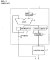
- the circuit is comprised of an address counter 1 and a function ROM 2.
- the address counter 1 is comprised of a first register 3, an adder 4, an accumulator 5, a control circuit 14 for inverting a bit, and a second register 7.
- Fig. 2 is a table showing an operation of the circuit.
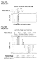
- Fig. 3A is a graph showing a relation between addresses of the function ROM 2 and amplitudes to be stored in the function ROM 2, found when a sine wave function is to be stored in the function ROM 2, and
- Fig. 3B shows waveforms of outputs transmitted from the function ROM 2 in the case that a numeral of 2 is stored in the first register 3.
- the adder 4 adds a value stored in the first register 3 to a value stored in the accumulator 5, and transmits the sum to the accumulator 5.
- the accumulator 5 latches the received sum at a sampling period.
- the control circuit 14 receives a first bit output transmitted from the adder 4.
- the first bit output is a bit output other than a second uppermost bit among bit outputs transmitted from the adder 4.
- the control circuit 14 inverts the received first bit output or allows the received first bit output to pass therethrough without inverted, in accordance with a second uppermost bit transmitted from the adder 4.
- An output transmitted from the control circuit 14 is latched by the second register 7 at a sampling period.
- the function ROM 2 stores therein a periodic function value associated with one-fourth of a period thereof.
- the periodic function value stored in the function ROM 2 can be read out by providing a value stored in the second register 7 which value has been operated by the address counter 1, to the function ROM 2 as an address.
- a combination of an output transmitted from the function ROM 2 and a lowermost bit transmitted from the accumulator 5 as an encoded bit constitutes an output of the periodic function.
- a function transmitted from the function ROM 2 in the above-mentioned circuit would have a frequency F as defined below, under the following conditions.
- the output frequency F is set to be equal to the sampling frequency fs multiplied by n/2 (p+2) , by varying the value n.
- the equation (A) indicates that even if an actual address of the function ROM 2 has p bits when a periodic function is to be generated, reading out the function ROM 2 is equivalent to reading out a function ROM having an address of (p+2) bits, and that a periodic function is generated by a period by virtue of a capacity of the function ROM 2, associated with one-fourth of a period of the function ROM 2.
- a sine wave function is selected as a periodic function. It is assumed that a minimum address in the function ROM 2 is defined as sin 0° , a maximum address in the function ROM 2 is defined as sin 90° , other addresses are defined as addresses obtained by equally dicretizing addresses ranging from the minimum address to the maximum, to thereby store a sine wave function having a quantized amplitude, into the function ROM 2.
- V (2 q -1) ⁇ sin (90° ⁇ (m/(2 P ⁇ 1)))
- the control circuit 14 inverts an address to be input into the function ROM 2, or allows the address to pass therethrough without inverting.
- the second example has an object to prevent the above-mentioned distortion in a frequency plane.
- a turning point in addresses including a maximum address and a minimum address appearing subsequently to the maximum address in the function ROM 2 it is assumed that values of a sine wave function are to be stored into the function ROM 2 at a phase angle having an offset relative to a sampling clock by a half period of the sampling clock.
- zero cross points in a resultant sine wave are located at a center between sampling clocks between second and third quadrants and also between fourth and first quadrants.
- the above-mentioned distortion in a frequency plane would not be generated.
- V (2 q -1) x sin (90° ⁇ ((2m + 1)/2 P+1 ))
- a resultant periodic function would include distortion in an amplitude plane.
- the conventional circuit for generating a periodic function is accompanied with problems of distortion in a frequency plane in a resultant periodic function, distortion in an amplitude plane or a phase difference between a resultant periodic function and a sampling clock.
- a circuit for digitally generating a series of encoded sampling values of a periodic function by virtue of ROM table conversion including (a) a function ROM in which an amplitude associated with one-fourth of a period of a periodic function is stored, and (b) an address counter which generates an address signal to be input into the function ROM, the address counter including (b1) an accumulator, (b2) a first register which is externally controllable, (b3) an adder which adds an output transmitted from the accumulator to an output transmitted from the first register, and transmits the sum to the accumulator, characterized in that the address counter further includes (b4) an address-conversion circuit which receives a first output transmitted from the adder, and converts the first output into the address signal, the first output being a bit output other than a second uppermost bit output among bit outputs transmitted from the adder, (b5) a second register which stores therein an output transmitted from the address-conversion circuit, and (b6) a zero-cross flag control circuit which
- the address-conversion circuit receives a bit output other than a second uppermost bit output among bit outputs transmitted from the adder, and converts the bit output in accordance with the second uppermost bit output among bit outputs transmitted from the adder.
- the address-conversion circuit includes (a) a first logic which inverts bit outputs bit by bit other than a second uppermost bit output among bit outputs transmitted from the adder, if a second uppermost bit output among bit outputs transmitted from the adder is equal to one, and allows bit outputs other than a second uppermost bit output among bit outputs transmitted from the adder, to pass therethrough as they are, if a second uppermost bit output among bit outputs transmitted from the adder is equal to zero, and (b) a second logic which adds an output transmitted from the first logic to a second uppermost bit output among bit outputs transmitted from the adder, at a lowermost bit.
- the zero-cross flag control circuit includes a controller which receives an uppermost bit output transmitted from the accumulator, and makes logic control, based on judgement made by the second register for all bit outputs.
- the zero-cross flag control circuit includes (a) a third logic which judges whether bit outputs transmitted from the second register are all equal to zero, and (b) a fourth logic which transmits an output indicative of zero regardless of an uppermost bit output transmitted from the accumulator, if all bit outputs transmitted from the second register are equal to zero, and allows an uppermost bit output transmitted from the accumulator, to pass therethrough as it is, if all bit outputs transmitted from the second register are not equal to zero.
- the amplitude is stored in the function ROM on the assumption that a minimum address in the address regions of the function ROM corresponds to a phase angle of 0 degree in a periodic function having a period consisting of a phase angle of 360 degrees, a maximum address in the address regions of the function ROM corresponds to a phase angle of 90 degrees in the periodic function, and each of addresses intermediate between the minimum and maximum addresses corresponds to a phase angle obtained by equally discretizing phase angles ranging from the minimum phase angle to the maximum phase angle.
- the above-mentioned periodic function includes a sine wave function, a function having a waveform a period of which is in point symmetry and a half period of which is in line symmetry, and a function having a waveform a period of which is in line symmetry and a half period of which is in point symmetry.
- a circuit for digitally generating a series of encoded sampling values of a periodic function by virtue of ROM table conversion including (a) a function ROM in which an amplitude associated with one-fourth of a period of a periodic function is stored, and (b) an address counter which generates an address signal to be input into the function ROM, the address counter including (b1) an accumulator, (b2) a first register which is externally controllable, (b3) an adder which adds an output transmitted from the accumulator to an output transmitted from the first register, and transmits the sum to the accumulator, (b4) an address-conversion circuit receives a first output transmitted from the accumulator, and converts the first output into the address signal, the first output being a bit output other than a second uppermost bit output among bit outputs transmitted from the accumulator, (b5) a second register which stores therein an output transmitted from the address-conversion circuit, (b6) a third register which stores therein an uppermost bit output transmitted from the
- the address-conversion circuit receives a bit output other than a second uppermost bit output among bit outputs transmitted from the accumulator, and converts the bit output in accordance with a second uppermost bit output among bit outputs transmitted from the accumulator.
- the address-conversion circuit includes (a) a first logic which inverts bit outputs bit by bit other than a second uppermost bit output among bit outputs transmitted from the accumulator, if a second uppermost bit output among bit outputs transmitted from the accumulator is equal to one, and allows bit outputs other than a second uppermost bit output among bit outputs transmitted from the accumulator, to pass therethrough as they are, if a second uppermost bit output among bit outputs transmitted from the accumulator is equal to zero, and (b) a second logic which adds an output transmitted from the first logic to a second uppermost bit output among bit outputs transmitted from the accumulator, at a lowermost bit.
- the zero-cross flag control circuit includes a controller which receives an output transmitted from the third register, and makes logic control, based on judgement made by the second register for all bit outputs.
- the zero-cross flag control circuit includes (a) a third logic which judges whether bit outputs transmitted from the second register are all equal to zero, and (b) a fourth logic which transmits an output indicative of zero regardless of an output transmitted from the third register, if all bit outputs transmitted from the second register are equal to zero, and allows an output transmitted from the third register, to pass therethrough as it is, if all bit outputs transmitted from the second register are not equal to zero.
- the amplitude is stored in the function ROM on the assumption that a minimum address in the address regions of the function ROM corresponds to a phase angle of 0 degree in a periodic function having a period consisting of a phase angle of 360 degrees, a maximum address in the address regions of the function ROM corresponds to a phase angle of 90 degrees in the periodic function, and each of addresses intermediate between the minimum and maximum addresses corresponds to a phase angle obtained by equally discretizing phase angles ranging from the minimum phase angle to the maximum phase angle.
- the circuit in accordance with the present invention is designed to include the address-conversion circuit and the zero-cross flag control circuit in place of the control circuit for inverting a bit, in the conventional circuit for generating a periodic function, to thereby optimize storage of an amplitude into the function ROM.
- the circuit includes a function ROM capacity associated with one-fourth of a period which capacity is almost the same as that of the conventional circuit, it is possible to generate a periodic function including no distortion in a frequency plane, no distortion in an amplitude plane and no phase difference between a resultant periodic function and a sampling clock.
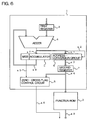
- Fig. 6 illustrates a circuit for generating a periodic function, in accordance with the first embodiment.
- the circuit is comprised of an address counter 1 and a function ROM 2 storing therein an amplitude of a resultant periodic function.
- the address counter 1 is comprised of a first register 3 into which a value can be externally input, an adder 4, an accumulator 5, a circuit 6 for converting an address, a second register 7, and a zero-cross flag control circuit 8.
- the adder 4 adds an output signal transmitted from the first register 3 to an output signal a8 transmitted from the accumulator 5, and transmits a signal a7 indicative of the sum, to the accumulator 5.
- the accumulator 5 latches the received signal a7 by a sampling clock at a sampling period.
- the address-conversion circuit 6 receives a signal a1 which is a signal other than a second uppermost bit output among the output signals a7 transmitted from the adder 4, and converts the signal a1 into a signal a3 having bits greater in number than bits of the signal a1 by one, in accordance with a signal a2 which is a second uppermost bit output among the output signals a7 transmitted from the adder 4.
- the thus converted signal a3 is transmitted to the second register 7.
- the second register 7 latches the signal a3 by a sampling clock at a sampling period, and transmits an output signal a4 to both the function ROM 2 and the zero-cross flag control circuit 8.
- the zero-cross flag control circuit 8 receives a signal a5 which is an uppermost bit output (MSB) transmitted from the accumulator 5, and controls a logic of the received signal a5 in accordance with the output signal a4 transmitted from the second register 7.
- MSB uppermost bit output
- the function ROM 2 stores an amplitude associated with one-fourth of a period of a periodic function, in each of addresses. An amplitude associated with each of addresses can be read out by transmitting the output signal a4 to the function ROM 2 from the second register 7 which output signal a4 is an address signal operated by the address counter 1.
- a combination of an output signal a9 transmitted from the function ROM 2 and an output signal a6 transmitted from the zero-cross flag control circuit 8 as an encoded bit constitutes a series of encoded sampling values in a period of the periodic function.
- the output signal a7 transmitted from the adder 4 and the output signal a8 transmitted from the accumulator 5 are both 4-bit signals
- the signal a1 is a 2-bit signal
- the signals a2, a5 and a6 are 1-bit signals
- the signals a3 and a4 are 3-bit signals
- the signal a9 is a 5-bit signal if an amplitude thereof is quantized in five bits.
- the number of bits of the signals a3 and a4 is equal to the number of bits of the signal a7 from which two (2) is subtracted and to which one (1) is added.
- a sine wave function is to be generated as a periodic function, and that an amplitude associated with sin 90° is stored in a maximum address among (2 P + 1) number of address regions where P indicates the number of bits other than a second uppermost bit output among output bits transmitted from the adder 4, and amplitudes quantized in accordance with a series of sampling values obtained by equally discretizing phase angles ranging from 0 degree to 90 degrees are stored in other addresses.
- the number of bits of the signal a4 acting as an address signal to be input into the function ROM 2 has to be equal to the number of bits of the output signal a7 from which two (2) is subtracted and to which one (1) is added. Since the signal a3 is input into the second register 7 and is output from the second register 7 as the output signal a4, the signals a3 and a4 have the same number of bits.
- V (2 q -1) ⁇ sin (90° ⁇ (m/(2 P-1 ))
- Fig. 7A illustrates amplitudes in one-fourth of a period in the first quadrant in a sine wave function to be stored in addresses 0 to 4 of the function ROM 2.
- Fig. 9 shows an internal operation of the circuit illustrated in Fig. 6 in the case that a value of 1 is stored in the first register 3.
- the zero-cross flag control circuit 8 judges that the output signal a4 transmitted from the second register 7 has 3 bits (000) by which sin 0° of the function ROM 2, that is, zero-cross points of the sine wave function, can be read out, the zero-cross flag control circuit 8 transmits a zero signal regardless of the signal a5 transmitted from the accumulator 5.
- the zero-cross flag control circuit 8 judges that the output signal a4 does not have 3 bits (000)
- the zero-cross flag control circuit 8 allows the signal a5 to pass therethrough as the output signal a6 which acts as an encoded bit for the output signal a9 transmitted from the function ROM 2.
- Fig. 8 is a block diagram illustrating structures of the address-conversion circuit 6 and the zero-cross flag control circuit 8.
- the address-conversion circuit 6 is comprised of an exclusive OR operation device 9 and an adder 10.
- the zero-cross flag control circuit 8 is comprised of a comparator 11 and a zero-cross flag switch 12.
- the exclusive OR operation device 9 inverts the signal a1 in each of bits, and the adder 10 adds one (1) to a lowermost bit output in outputs transmitted from the exclusive OR operation device 9.
- To add one (1) to a lowermost bit output in outputs transmitted from the exclusive OR operation device 9 is conducted by the adder 10 not by actually adding a figure 1 to the lowermost bit output, but by directly adding the output signal a2 to the lowermost bit output.
- An output signal a 3 transmitted from the adder 10 has 3 bits greater than the bits of the signal a1 by one bit, and is latched by the second register 7 at a timing of a sampling clock. As a result, the output signal a3 is converted into a signal a4 having 3 bits, which is input into the comparator 11 in the zero-cross flag control circuit 8.
- the zero-cross flag control circuit 8 stores a 3-bit value (000) therein as a reference value.
- the comparator 11 transmits a signal indicative of one (1), whereas when the received signal a4 is not coincident with the reference value, the comparator 11 transmits a signal indicative of zero (0).
- the comparator 11 detects a 3-bit value (000) in the address signal a4, which value is associated with a zero-cross point in a sine wave function.
- the zero-cross flag switch 12 is switched. Specifically, when the zero-cross flag switch 12 receives a signal indicative of zero from the comparator 11, the zero-cross flag switch 12 allows the signal a5 to pass therethrough without being inverted, whereas when the zero-cross flag switch 12 receives a signal indicative of one from the comparator 11,the zero-cross flag switch 12 transmits a signal indicative of zero. Thus, the zero-cross flag switch 12 transmits a 1-bit signal a6.
- the signal a6 acts as an encoded bit where 0 indicates a positive value and 1 indicates a negative value.
- the signals a4 as shown in Fig. 4 are read out as addresses to be input into the function ROM 2, and combined with the signals a6, thereby the sine wave output illustrated in Fig. 7A can be obtained.
- a waveform of the sine wave output illustrated in Fig. 7B is characterized in that sampling clocks are coincident with zero-cross points of a sine wave, and that positive and negative maximum amplitudes can be obtained at maximum addresses of the function ROM 2.
- the output transmitted from the function ROM 2 in the above-mentioned circuit would have a frequency F as defined below, under the following conditions.
- the output frequency F is equal to the sampling frequency fs multiplied by n/2 (p+1) , by varying the value n.
- the equation (B) indicates that though only a periodic function having a one-fourth period is stored in the function ROM 2 having the ( 2 P-1 + 1 ) number of addresses, namely, address 0 to address 2 P-1 , reading out the function ROM 2 is equivalent to reading out a function ROM in which a periodic function having a period is stored in the 2 P+1 number of addresses. This advantage is brought by the address-conversion circuit 6 and the zero-cross flag control circuit 8.
- the equations (B) and (A) are equivalent to each other, because the number of address bits of the function ROM 2 is greater than by one bit that of the conventional one.
- the number of address bits in the first embodiment is greater by one than the conventional one, since the number of address regions in the function ROM 2 is equal to ( 2 (p-1) + 1 ), the address regions in the first embodiment are greater in number than the address regions in the conventional circuit only by one. Accordingly, in accordance with the first embodiment, it is possible to generate a periodic function having a period with a capacity of the function ROM 2 being almost the same as that in the conventional circuit.
- the circuit in accordance with the first embodiment is designed to include the address-conversion circuit 6 and the zero-cross flag control circuit 8 in place of the control circuit 14 for inverting a bit, which is a part of the conventional circuit for generating a periodic function, to thereby optimize storage of an amplitude into the function ROM 2.
- the circuit in accordance with the first embodiment provides the following advantages.
- the first advantage is that it is not necessary to increase a capacity of a function ROM having a one-fourth period relative to the same in the conventional circuit. This advantage is brought by the structure where the number of address regions in the function ROM 2 is greater only by one than the same in a function ROM in the conventional circuit.
- the second advantage is that no distortion is ensured in an amplitude plane. This advantage is brought by both the address-conversion circuit 6 and the zero-cross flag control circuit 8 both of which control addresses of the function ROM 2 such that function values at both zero-cross points and a maximum amplitude are flattened without distortion.
- the third advantage is that no distortion in a frequency plane and no phase difference between a resultant periodic function and a sampling clock are ensured. This advantage is brought by the structure in which maximum and minimum amplitudes of a resultant periodic function are stored in the function ROM 2.
- a sine wave function has been selected as a periodic function in the above-mentioned first embodiment, there may be selected a periodic function in which a period of a waveform is in point symmetry and a half period of a waveform is in line symmetry, or a periodic function in which a period of a waveform is in line symmetry and a half period of a waveform is in point symmetry.
- the present invention can be applied to such periodic functions by adjusting zero-cross points in the zero-cross flag control circuit 8.
- Fig. 10 illustrates a circuit for generating a periodic function, in accordance with the second embodiment.
- the circuit is comprised of an address counter 1 and a function ROM 2 storing therein an amplitude of a resultant periodic function.
- the address counter 1 is comprised of a first register 3 into which a value can be externally input, an adder 4, an accumulator 5, a circuit 6 for converting an address, a second register 7, a zero-cross flag control circuit 8, and a third register 13.
- the signals a1 and a2 which are both parts of the output signals a7 transmitted from the adder 4 are input into the address-conversion circuit 6.
- signals a10 other than a second uppermost bit output among the output signals a8 transmitted from the accumulator 5 which output signals a8 are delayed by a sampling clock are input into the address-conversion circuit 6 in place of the signal a1
- a second uppermost bit output signal a11 among the output signals a8 is input into the address-conversion circuit 6 in place of the signal a2.
- the third register 13 receives an uppermost bit output signal (MSB) a5 transmitted from the accumulator 5, latches the thus received signal a5 at a timing of a sampling clock, and transmits an output to the zero-cross flag control circuit 8.
- the third register 13 compensates for delay to a degree of a sampling clock which delay is generated in a path in which addresses to be input into the function ROM 2 are generated.
- An operation for generating a periodic function in the circuit in accordance with the second embodiment is the same as that of the circuit in accordance with the first embodiment except an operation of the third register 13.
- the reason why the address-conversion circuit 6 receives output signals transmitted from the accumulator 5 is as follows.
- the address-conversion circuit 6 is designed to directly receive outputs transmitted from the adder 4 as shown in the first embodiment, an operation might not be finished within a period of one sampling clock, because of increased operation volume.
- the circuit in accordance with the second embodiment solves this problem. Though total delay is increased, the circuit in accordance with the second embodiment provides a periodic function having high accuracy for an operation.
Landscapes
- Engineering & Computer Science (AREA)
- Theoretical Computer Science (AREA)
- Physics & Mathematics (AREA)
- General Engineering & Computer Science (AREA)
- General Physics & Mathematics (AREA)
- Electrophonic Musical Instruments (AREA)
- Stabilization Of Oscillater, Synchronisation, Frequency Synthesizers (AREA)
Abstract
Description
Claims (14)
- A circuit for digitally generating a series of encoded sampling values of a periodic function by virtue of ROM table conversion, comprising (a) a function ROM (2) in which an amplitude associated with one-fourth of a period of a periodic function is stored; and (b) an address counter (1) which generates an address signal to be input into the function ROM (2),the address counter (1) comprising (b1) an accumulator (5); (b2) a first register (3) which is externally controllable; and (b3) an adder (4) which adds an output (a8) transmitted from the accumulator (5) to an output transmitted from the first register (3), and transmits the sum (a7) to the accumulator (5),
characterized in that the address counter (1) is comprised further of:(b4) an address-conversion circuit (6) which receives a first output (a1) transmitted from the adder (4), and converts the first output (a1) into the address signal, the first output (a1) being a bit output other than a second uppermost bit output among bit outputs (a7) transmitted from the adder (4);(b5) a second register (7) which stores therein an output (a3) transmitted from the address-conversion circuit (6); and(b6) a zero-cross flag control circuit (8) which receives an uppermost bit output (a5) transmitted from the accumulator (5), and makes logic control,an output (a4) transmitted from the second register (7) being input into the function ROM (2) as the address signal,the function ROM (2) having the (2P + 1) number of address regions where P indicates the number of bits other than a second uppermost bit output among outputs (a7) transmitted from the adder (4),the series of encoded sampling values being defined as a sum of an output (a9) transmitted from the function ROM (2) and an output (a6) transmitted from the zero-cross flag control circuit (8). - The circuit as set forth in claim 1, wherein the address-conversion circuit (6) receives a bit output (a1) other than a second uppermost bit output (a2) among bit outputs (a7) transmitted from the adder (4), and converts the bit output (a1) in accordance with the second uppermost bit output (a2) among bit outputs (a7) transmitted from the adder (4).
- The circuit as set forth in claim 1, wherein the address-conversion circuit (6) includes:(a) a first logic (9) which inverts bit outputs (a1) bit by bit other than a second uppermost bit output (a2) among bit outputs (a7) transmitted from the adder (4), if a second uppermost bit output (a2) among bit outputs (a7) transmitted from the adder (4) is equal to one, and allows bit outputs (a1) other than a second uppermost bit output (a2) among bit outputs (a7) transmitted from the adder (4), to pass therethrough as they are, if a second uppermost bit output (a2) among bit outputs (a7) transmitted from the adder (4) is equal to zero; and(b) a second logic (10) which adds an output transmitted from the first logic (9) to a second uppermost bit output (a2) among bit outputs (a7) transmitted from the adder (4), at a lowermost bit.
- The circuit as set forth in claim 1, 2 or 3, wherein the zero-cross flag control circuit (8) includes a controller (12) which receives an uppermost bit output (a5) transmitted from the accumulator (5), and makes logic control, based on judgement made by the second register (7) for all bit outputs.
- The circuit as set forth in claim 1, 2 or 3, wherein the zero-cross flag control circuit (8) includes:(a) a third logic (11) which judges whether bit outputs (a4) transmitted from the second register (7) are all equal to zero; and(b) a fourth logic (12) which transmits an output indicative of zero regardless of an uppermost bit output (a5) transmitted from the accumulator (5), if all bit outputs (a4) transmitted from the second register (7) are equal to zero, and allows an uppermost bit output (a5) transmitted from the accumulator (5), to pass therethrough as it is, if all bit outputs (a4) transmitted from the second register (7) are not equal to zero.
- The circuit as set forth in claim 1, wherein the address counter (1) is comprised further of a third register (13) which stores therein an uppermost bit output (a5) transmitted from the accumulator (5), and wherein the address-conversion circuit (6) receives the first output (a10) transmitted from the accumulator (5), the zero-cross flag control circuit (8) receives an output transmitted from the third register (13), and the function ROM (2) has the (2P + 1) number of address regions where P indicates the number of bits other than a second uppermost bit output among outputs (a8) transmitted from the accumulator (5).
- The circuit as set forth in claim 6, wherein the address-conversion circuit (6) receives a bit output (a10) other than a second uppermost bit output (a11) among bit outputs (a8) transmitted from the accumulator (5), and converts the bit output (a10) in accordance with a second uppermost bit output (a11) among bit outputs (a8) transmitted from the accumulator (5).
- The circuit as set forth in claim 6, wherein the address-conversion circuit (6) includes:(a) a first logic (9) which inverts bit outputs (a10) bit by bit other than a second uppermost bit output (a11) among bit outputs (a8) transmitted from the accumulator (5), if a second uppermost bit output (a11) among bit outputs (a8) transmitted from the accumulator (5) is equal to one, and allows bit outputs (a10) other than a second uppermost bit output (a11) among bit outputs (a8) transmitted from the accumulator (5), to pass therethrough as they are, if a second uppermost bit output (a11) among bit outputs (a8) transmitted from the accumulator (5) is equal to zero; and(b) a second logic (10) which adds an output transmitted from the first logic (9) to a second uppermost bit output (a11) among bit outputs (a8) transmitted from the accumulator (5), at a lowermost bit.
- The circuit as set forth in claim 6, 7 or 8, wherein the zero-cross flag control circuit (8) includes a controller (12) which receives an output transmitted from the third register (13), and makes logic control, based on judgement made by the second register (7) for all bit outputs.
- The circuit as set forth in claim 6, 7 or 8, wherein the zero-cross flag control circuit (8) includes:(a) a third logic (11) which judges whether bit outputs (a4) transmitted from the second register (7) are all equal to zero; and(b) a fourth logic (12) which transmits an output indicative of zero regardless of an output transmitted from the third register (13), if all bit outputs (a4) transmitted from the second register (7) are equal to zero, and allows an output transmitted from the third register (13), to pass therethrough as it is, if all bit outputs (a4) transmitted from the second register (7) are not equal to zero.
- The circuit as set forth in claim 1, 2, 3, 6, 7 or 8, wherein the amplitude is stored in the function ROM (2) on the assumption that a minimum address in the address regions of the function ROM (2) corresponds to a phase angle of 0 degree in a periodic function having a period consisting of a phase angle of 360 degrees, a maximum address in the address regions of the function ROM (2) corresponds to a phase angle of 90 degrees in the periodic function, and each of addresses intermediate between the minimum and maximum addresses corresponds to a phase angle obtained by equally discretizing phase angles ranging from the minimum phase angle to the maximum phase angle.
- The circuit as set forth in claim 1, 2, 3, 6, 7 or 8, wherein the periodic function is a sine wave function.
- The circuit as set forth in claim 1, 2, 3, 6, 7 or 8, wherein the periodic function have a waveform a period of which is in point symmetry and a half period of which is in line symmetry.
- The circuit as set forth in claim 1, 2, 3, 6, 7 or 8, wherein the periodic function have a waveform a period of which is in line symmetry and a half period of which is in point symmetry.
Applications Claiming Priority (2)
| Application Number | Priority Date | Filing Date | Title |
|---|---|---|---|
| JP01696099A JP3226884B2 (en) | 1999-01-26 | 1999-01-26 | Periodic function generator |
| JP1696099 | 1999-01-26 |
Publications (2)
| Publication Number | Publication Date |
|---|---|
| EP1030238A2 true EP1030238A2 (en) | 2000-08-23 |
| EP1030238A3 EP1030238A3 (en) | 2005-01-12 |
Family
ID=11930688
Family Applications (1)
| Application Number | Title | Priority Date | Filing Date |
|---|---|---|---|
| EP00101451A Withdrawn EP1030238A3 (en) | 1999-01-26 | 2000-01-25 | Circuit for generating a periodic function |
Country Status (4)
| Country | Link |
|---|---|
| US (1) | US6519619B1 (en) |
| EP (1) | EP1030238A3 (en) |
| JP (1) | JP3226884B2 (en) |
| KR (1) | KR100341163B1 (en) |
Families Citing this family (2)
| Publication number | Priority date | Publication date | Assignee | Title |
|---|---|---|---|---|
| JP2002182898A (en) | 2000-12-14 | 2002-06-28 | Nec Microsystems Ltd | Method and circuit for generating integrated value and period function |
| KR20040015457A (en) * | 2002-08-13 | 2004-02-19 | 현대모비스 주식회사 | Method for controlling tasks having different controlling period |
Family Cites Families (6)
| Publication number | Priority date | Publication date | Assignee | Title |
|---|---|---|---|---|
| US3772681A (en) * | 1970-10-14 | 1973-11-13 | Post Office | Frequency synthesiser |
| JPS6037486A (en) | 1983-08-06 | 1985-02-26 | 三菱重工業株式会社 | Method of construction of quick burying joint of undergroundburied steel pipe |
| JPH0656555B2 (en) * | 1986-09-05 | 1994-07-27 | ヤマハ株式会社 | Sound generator |
| JPH0743620A (en) | 1993-07-29 | 1995-02-14 | Olympus Optical Co Ltd | Illuminating optical system for endoscope and illuminating lens |
| US5937438A (en) * | 1997-06-30 | 1999-08-10 | Lucent Technologies Inc. | Sine/cosine lookup table |
| US5892692A (en) * | 1997-10-01 | 1999-04-06 | Ford Motor Company | Method for generating a lookup table for a digital oscillator |
-
1999
- 1999-01-26 JP JP01696099A patent/JP3226884B2/en not_active Expired - Fee Related
-
2000
- 2000-01-21 US US09/488,531 patent/US6519619B1/en not_active Expired - Fee Related
- 2000-01-25 KR KR1020000003457A patent/KR100341163B1/en not_active Expired - Fee Related
- 2000-01-25 EP EP00101451A patent/EP1030238A3/en not_active Withdrawn
Also Published As
| Publication number | Publication date |
|---|---|
| JP3226884B2 (en) | 2001-11-05 |
| EP1030238A3 (en) | 2005-01-12 |
| KR20000076518A (en) | 2000-12-26 |
| JP2000215029A (en) | 2000-08-04 |
| US6519619B1 (en) | 2003-02-11 |
| KR100341163B1 (en) | 2002-06-20 |
Similar Documents
| Publication | Publication Date | Title |
|---|---|---|
| US6324235B1 (en) | Asynchronous sample rate tracker | |
| CA1149289A (en) | Adpcm system for speech or like signals | |
| NL8501956A (en) | IMAGE RECOVERY CIRCUIT. | |
| JPH04310072A (en) | Video signal clamp circuit | |
| US5017920A (en) | High-speed modified successive approximation analog to digital converter | |
| US6330578B1 (en) | Method and apparatus for digitally representing a waveform | |
| JPS5825784A (en) | Digital method and device for calibrating phase error of sample signal applicable for calibration of television signal | |
| US4412220A (en) | Digital scan converter | |
| EP1030238A2 (en) | Circuit for generating a periodic function | |
| AU625793B2 (en) | Phase accumulator with dithered incrementing of accumulation due to fine phase components | |
| US4855745A (en) | High resolution analog-to-digital converter | |
| US4811370A (en) | Digital muting circuit | |
| EP0632459B1 (en) | Delay circuit using a digital memory | |
| US4549305A (en) | Adaptive differential PCM decoder | |
| JPH11326493A (en) | Radar video transmission device, digital transmitter and receiver | |
| JP2584437B2 (en) | A / D conversion circuit | |
| US6952174B2 (en) | Serial data interface | |
| JPS6251539B2 (en) | ||
| JP3202390B2 (en) | Waveform observation device | |
| JP3634934B2 (en) | Modulation circuit, demodulation circuit, and modulation / demodulation system | |
| KR900008449B1 (en) | Delaying circuit of digital signal | |
| JP2658038B2 (en) | Digital-to-analog converter | |
| EP0549069B1 (en) | Image motion detecting device for an image processing system and the method thereof | |
| JP2954013B2 (en) | A / D converter | |
| JP2599984B2 (en) | Input data peak value detection circuit |
Legal Events
| Date | Code | Title | Description |
|---|---|---|---|
| PUAI | Public reference made under article 153(3) epc to a published international application that has entered the european phase |
Free format text: ORIGINAL CODE: 0009012 |
|
| AK | Designated contracting states |
Kind code of ref document: A2 Designated state(s): AT BE CH CY DE DK ES FI FR GB GR IE IT LI LU MC NL PT SE |
|
| AX | Request for extension of the european patent |
Free format text: AL;LT;LV;MK;RO;SI |
|
| RAP1 | Party data changed (applicant data changed or rights of an application transferred) |
Owner name: NEC ELECTRONICS CORPORATION |
|
| PUAL | Search report despatched |
Free format text: ORIGINAL CODE: 0009013 |
|
| AK | Designated contracting states |
Kind code of ref document: A3 Designated state(s): AT BE CH CY DE DK ES FI FR GB GR IE IT LI LU MC NL PT SE |
|
| AX | Request for extension of the european patent |
Extension state: AL LT LV MK RO SI |
|
| 17P | Request for examination filed |
Effective date: 20041202 |
|
| AKX | Designation fees paid |
Designated state(s): DE FR GB IT NL |
|
| STAA | Information on the status of an ep patent application or granted ep patent |
Free format text: STATUS: THE APPLICATION HAS BEEN WITHDRAWN |
|
| 18W | Application withdrawn |
Effective date: 20051005 |