The present invention relates to a semiconductor laser-excitation solid-state
laser oscillating device (a solid-state laser oscillating device using
semiconductor lasers as excitation source, also called an LD-excitation solid-state
laser oscillating device) for use in a laser beam machining apparatus, etc.
A semiconductor laser-excitation solid-state laser oscillating device
having semiconductor lasers arranged around a solid-state laser medium such
as YAG has advantages of high efficiency of oscillation as compared with a
conventional one of a lamp excitation type, and has a compact size to lower a
burden of maintenance, and therefore research and development of this device
is carried on for widespread use in the industry.
Generally speaking, rising of a laser output of the solid-state laser
oscillating device of light excitation system follows the input of excitation
light with a considerable time lag. However, in the so-called high-output
solid-state laser oscillating device excited by LD of kW class, a gain is
sufficiently high and the time lag between an input of the excitation light and a
rising of laser beam output is so small as to be actually neglected. The
semiconductor laser to be used as an excitation light source falls into two
types; a continuous oscillation type and a pulse type.
Corresponding to these two types of excitation sources, the output
waveform obtained by the conventional solid-state laser oscillator excited by
semiconductor laser is basically either of a pulse type or of a continuous
oscillation type.
However, an output waveform obtained by the conventional
semiconductor laser-excitation solid-state laser oscillating device has great
restrictions and an improvement in this device has been desired. First, in the
semiconductor laser-excitation solid-state laser oscillating device of the pulse
type, the obtained output beam has a very narrow pulse width (for example,
0.4 msec) which poses a problem in practical use. In the case where the device
of this type is to be applied to welding of aluminum, for example, a longer
pulse (for example, 1 msec or more) is required. Therefore, the conventional
solid-state laser oscillating device using the semiconductor laser of pulse type
as the excitation source cannot be used for this purpose.
On the other hand, in the solid-state laser oscillating device using the
semiconductor lasers of continuous-oscillation type as the excitation source, a
laser output having a desired pulse width can be obtained by modulating
driving current of the semiconductor lasers into a pulse shape. However, in
this method the continuous output is interrupted, so that a surplus portion
remains in the input energy to the semiconductor lasers of continuous-driving
type. Accordingly, the average output of the solid-state laser oscillator
decreases. To compensate this decrease, the number of arranged
semiconductor lasers has to be increased, to make the device disadvantageous.
In addition to the above problem, there is a problem that it is difficult
to design an output waveform in accordance with the application. In the case
where a stepwise output waveform is required, for example, it is
conventionally adopted a method in which the input current to the
semiconductor lasers of pulse type is changed stepwise. In this case as well,
the semiconductor lasers used as an excitation source do not take full
advantage of their capability, so that a surplus portion remains in the input
energy. Accordingly, the average output of the solid-state laser oscillator
decreases. To compensate this decrease, the number of arranged
semiconductor lasers has to be increased.
An object of the present invention is to improve a semiconductor laser-excitation
solid-state laser oscillating device so as to obtain a desired output
waveform by efficiently utilizing capability of semiconductor lasers used as an
excitation source, thus enhancing industrial usability of the
semiconductor laser-excitation solid-state laser oscillating device.
The present invention is applied to a semiconductor laser-excitation
solid-state laser oscillating device comprising a solid-state laser medium
arranged in an optical resonator, an excitation light source for laser-exciting
the solid-state laser medium and a controller for controlling the excitation light
source.
According to the basic feature of the present invention, the excitation
light source includes semiconductor lasers divided into a plurality of groups
and the controller controls the excitation light source so that on/off timing of
the excitation light from the semiconductor lasers in at least one group are
different from on/off timing of the semiconductor lasers in another group so as
to obtain a laser output having a predetermined waveform from the solid-state
laser medium.
In one typical case, all the semiconductor lasers in the groups are of
pulse type. In this case, it is preferable that the semiconductor lasers in each
group have the same maximum driving current, the same maximum pulse
width and the same maximum duty cycle (the same characteristics in each
group).
In another typical case, the semiconductor lasers in at least one group
are of continuous-output type and the semiconductor lasers in the remaining
groups are of pulse type. In this case, it is preferable that the semiconductor
lasers in at least one group have the same maximum driving current, and the
semiconductor lasers in the remaining groups have the same maximum driving
current, the same pulse width and the same maximum duty cycle (the same
characteristics in each group).
In the case where the semiconductor lasers used in each of the
semiconductor laser groups have the same characteristics, the controller may
control driving current, pulse width and repetition frequency of the pulse-type
semiconductor lasers in at least two groups independently with respect to
respective groups to settle leading edges of pulses of the excitation light.
In this case, assuming that N (N≥2) groups of pulse-type
semiconductor lasers having pulse width of ΔT are provided, the controller may
control the pulse-type semiconductor lasers in n-th group so that on-timing of
the pulse-type semiconductor lasers in the n-th group delays substantially by
nΔT with respect to on-timing of the pulse-type semiconductor lasers in the first
group. With this arrangement, there remains no surplus of excitation input, so
that an output having a substantially expanded pulse width can be obtained.
BRIEF DESCRIPTION OF THE DRAWINGS
FIG. 1 is a schematic view showing an example of a semiconductor
laser-excitation solid-state laser oscillating device according to the present
invention;
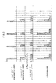
FIG. 2 is a time chart showing control of semiconductor lasers and an
output waveform according to a first embodiment;
FIG. 3 is a flowchart showing an outline of processing in the first
embodiment;
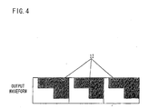
FIG. 4 is a diagram showing a surplus in input energy in the
conventional device for obtaining an output waveform equivalent to that in the
first example;
FIG. 5 is a time chart for showing control of the semiconductor lasers
and an output waveform according to a second embodiment;
FIG. 6 is a flowchart showing an outline of processing in the second
embodiment;
FIG. 7 is a diagram showing a surplus in input energy in the
conventional system for obtaining an output waveform equivalent to that in the
second embodiment;
FIG. 8 is a time chart showing control of the semiconductor lasers and
an output waveform according to a third embodiment;
FIG. 9 is a flowchart showing an outline of processing in the third
embodiment; and
FIG. 10 is a graph representing a relationship between the number of
groups and the obtained peak output and pulse width in the third example.
FIG. 1 is a schematic view showing a basic part of a semiconductor
laser-excitation solid-state laser oscillating device according to an embodiment
of the present invention. Referring to FIG. 1, a solid-state laser medium 3 is
disposed in an optical resonator composed of an output coupler (partially
reflective mirror) 1 and a rear mirror (totally reflective mirror) 2, and an
appropriate number (twelve in this figure) of LD (laser diode) stacks are
arranged around the laser medium 3. The solid-state laser medium 3 is, for
example, a flat slab shaped Nd:YAG laser crystal. Although not shown in this
figure, both end faces of the laser medium 3 are preferably cut obliquely with
respect to the thickness direction so as to have an angle substantially meeting
Brewster's condition. Sometimes, a rod shaped laser crystal is used.
Each of a total of twelve LD stacks has a predetermined number of
semiconductor laser elements (generally, one or more LD elements) as a unit.
Here, the LD stacks are divided into three groups denoted by reference
numbers 4, 5 and 6. Hereinafter, these groups (semiconductor laser groups)
are called a first group, a second group, and a third group in that order. Four
LD stacks 4 constitute the semiconductor lasers of first group. Similarly, four
LD stacks 5 constitute the semiconductor lasers of second group, and four LD
stacks 6 constitute the semiconductor lasers of third group. The reason for
distributed arrangement of four LD stacks of the same group is to stabilize the
laser output. Other arrangements are permitted.
Each of the LD stacks of each group is connected to a control circuit 7
incorporating a power source. The control circuit 7 is further connected to a
central processing unit (I/O built-in) 8 provided with a memory 9. In the
memory 9, programs for controlling each semiconductor laser of each group in
a later-described modes and related set values have been written. Although
not shown in the figure, a control section composed of the control circuit 7, the
central processing unit 8, and the memory 9 is provided, as necessary, with an
operation section for executing the input of programs and parameters, edit,
setting, and the like manually.
When the semiconductor lasers equipped in the LD stacks 4, 5 and 6
emit light by means of an input current from the control section, the solid-state
laser medium 3 is laser-excited, so that a laser beam 10 is generated. The laser
beam 10 is taken out via the output coupler (partially reflective mirror) 1, and
is used as a laser output beam 11 for laser machining, for example. The light
emitting progress on which the semiconductor lasers equipped in the LD
stacks 4, 5 and 6 are caused to emit light will be described later.
For the semiconductor lasers equipped in the LD stacks 4, 5 and 6,
their types (classification of pulse type and continuous oscillation type) and
characteristics are uniformed for each semiconductor group to which they
belong. The uniformed characteristics for the pulse type semiconductor laser
are the maximum driving current, the maximum pulse width, and the
maximum duty cycle. The uniformed characteristics for the continuous output
type semiconductor laser are the maximum driving current.
The type (classification of pulse type and continuous oscillation type)
and characteristics (maximum driving current, maximum pulse width,
maximum duty cycle) of semiconductor laser of each group and the specific
details of control are determined according to the waveform (the time progress
pattern of power) desired as the laser beam output 11. The following is a
description of the basic points of some examples.
[First Embodiment]
(Type and characteristics of each group)
- First group:
- Continuous oscillation type; maximum driving current i1
- Second group:
- Pulse type; maximum driving current i2; maximum pulse width
ΔT; maximum duty cycle 1/6 ΔT
- Third group:
- Pulse type; maximum driving current i3; maximum pulse width
2ΔT; maximum duty cycle 1/6 ΔT
(Control details)
The input current to the semiconductor laser of each group is
controlled according to a time chart of FIG. 2. Specifically, the continuous
oscillation type semiconductor laser of the first group is continuously
oscillated with the maximum driving current i1. Also, the pulse type
semiconductor laser of the second group is oscillated with the maximum
driving current i2 and the maximum pulse width ΔT, and the pulse type
semiconductor laser of the third group is oscillated with the maximum driving
current i3 and the maximum pulse width 2ΔT.
As shown in the chart, control is carried out so that the ON timing
shifts by ΔT to pulse-oscillate the second group and the third group one after
another.
FIG. 3 is a flowchart showing the outline of processing performed by
the central processing unit 8. The basic point of each step is as described
below.
Step S1: The continuous oscillation of the semiconductor lasers
belonging to the first group is turned ON (the driving current i1 supply start
command is outputted).
Step S2: Immediately after Step S1, the pulse oscillation of the
semiconductor lasers belonging to the second group is turned ON (driving
current i2, pulse width ΔT).
Step S3: After ΔT has elapsed, the control proceeds to Step S4.
Step S4: The pulse oscillation of the semiconductor lasers belonging to
the third group is turned ON (driving current i3, pulse width 2ΔT).
Step S5: After 5ΔT has elapsed, the control proceeds to Step S6.
Step S6: The presence of laser output OFF command is checked. If the
laser output OFF command has been given, the OFF command of the driving
current i1 of the semiconductor lasers belonging to the first group is issued,
and the processing is ended. In other cases, the control returns to Step S2.
When such control is carried out, letting the number of semiconductor
lasers belonging to the first, second, and third groups be g
1, g
2 and g
3,
respectively, the current (first one cycle) inputted for laser excitation is given
as described below. The ON time (oscillation start time) of the first group is
taken as t=0.
Given g1 = g2 = g3, the obtained laser output is as shown at the bottom
of the time chart of FIG. 2. Specifically, an output waveform (time progress of
output) in which the pulse output components are superposed on the
continuous output component can be obtained. If an attempt is made to obtain
the output waveform equivalent to this by using the conventional system, a
continuous oscillation type semiconductor laser is used, and it is modulated on
the progress of the same waveform. In this case, an excess portion (hatched
portion; the capability of semiconductor laser is not brought into play) 12 as
shown in FIG. 4 is generated. Such an output waveform is very useful in laser
beam machining of some kind.
[Second Embodiment]
(Type and characteristics of each group)
- First group:
- pulse type; maximum driving current j1; maximum pulse width
ΔT/2; maximum duty cycle 1/6 ΔT
- Second group:
- pulse type; maximum driving current j2; maximum pulse width
ΔT; maximum duty cycle 1/6 ΔT
- Third group:
- pulse type; maximum driving current j3; maximum pulse width
2ΔT; maximum duty cycle 1/6 ΔT
(Control details)
The input current to the semiconductor lasers of each group is
controlled according to a time chart of FIG. 5. Specifically, the pulse type
semiconductor laser of the first group is oscillated with the maximum driving
current ji and the maximum pulse width ΔT/2. The pulse type semiconductor
laser of the second group is oscillated with the maximum driving current j2 and
the maximum pulse width ΔT, and the pulse type semiconductor laser of the
third group is oscillated with the maximum driving current j3 and the
maximum pulse width 2ΔT.
As shown in the chart, the pulse oscillation of the first and second
groups is turned ON at the same time, but control is carried out so that the ON
timing of the third group shifts by ΔT/2 with respect to the first group (and
second group).
FIG. 6 is a flowchart showing the outline of processing performed by
the central processing unit 8. The basic point of each step is as described
below.
Step M1: The pulse oscillation of the semiconductor lasers belonging
to the first group is turned ON (driving current j1, pulse width ΔT/2).
Step M2: Immediately after Step Ml, the pulse oscillation of the
semiconductor lasers belonging to the second group is turned ON (driving
current j2, pulse width ΔT).
Step M3: After ΔT/2 has elapsed, the control proceeds to Step M4.
Step M4: The pulse oscillation of the semiconductor lasers belonging
to the third group is turned ON (driving current j3, pulse width 2ΔT).
Step M5: After 11ΔT/2 has elapsed, the control proceeds to Step M6.
Step M6: The presence of laser output OFF command is checked. If
the laser output OFF command has been given, the processing is ended. In
other cases, the control returns to Step Ml.
When such control is carried out, letting the number of semiconductor
lasers belonging to the first, second, and third groups be g
1, g
2 and g
3,
respectively, the current (first one cycle) inputted for laser excitation is given
as described below. The ON time (oscillation start time) of the first group is
taken as t=0.
Given g1 = g2 = g3, the obtained laser output is as shown at the bottom
of the time chart of FIG. 5. Specifically, a stepwise pulse output waveform
(time progress of output) in which the pulse output components of three
groups are superposed one after another can be obtained. If an attempt is
made to obtain the laser output equivalent to this by using the conventional
system, a continuous oscillation type semiconductor laser is used, and it is
modulated on the progress of the same waveform. In this case, an excess
portion (hatched portion; the capability of semiconductor laser is not brought
into play) 12 as shown in FIG. 7 is generated. Such an output waveform is
also very useful in laser beam machining of some kind.
[Third Embodiment]
(Type and characteristics of each group)
- First group:
- Pulse type; maximum driving current k1; maximum pulse width
ΔT; maximum duty cycle 1/6 ΔT
- Second group:
- Pulse type; maximum driving current k2; maximum pulse width
ΔT; maximum duty cycle 1/6 ΔT
- Third group:
- Pulse type; maximum driving current k3; maximum pulse width
ΔT; maximum duty cycle 1/6 ΔT
(Control details)
The input current to the semiconductor lasers of each group is
controlled according to a time chart of FIG. 8. Specifically, the pulse type
semiconductor laser of the first group is oscillated with the maximum driving
current k1 and the maximum pulse width ΔT. The pulse type semiconductor
laser of the second group is oscillated with the maximum driving current k2
and the maximum pulse width ΔT, and the pulse type semiconductor laser of
the third group is oscillated with the maximum driving current k3 and the
maximum pulse width ΔT.
As shown in the time chart, control is carried out so that the ON timing
of the first, second, and third groups shifts by ΔT.
FIG. 9 is a flowchart showing the outline of processing performed by
the central processing unit 8. The basic point of each step is as described
below.
Step D1: The pulse oscillation of the semiconductor lasers belonging
to the first group is turned ON (driving current k1, pulse width ΔT).
Step D2: After ΔT has elapsed, the control proceeds to Step D3.
Step D3: The pulse oscillation of the semiconductor lasers belonging
to the second group is turned ON (driving current k2, pulse width ΔT).
Step D4: After ΔT has elapsed, the control proceeds to Step D5.
Step D5: The pulse oscillation of the semiconductor lasers belonging
to the third group is turned ON (driving current k3, pulse width ΔT).
Step D6: After 4ΔT has elapsed, the control proceeds to Step M7.
Step D7: The presence of laser output OFF command is checked. If
the laser output OFF command has been given, the processing is ended. In
other cases, the control returns to Step D1.
When such control is carried out, letting the number of semiconductor
lasers belonging to the first, second, and third groups be g
1, g
2 and g
3,
respectively, the current (first one cycle) inputted for laser excitation is given
as described below. The ON time (oscillation start time) of the first group is
taken as t=0.
Given g1 = g2 = g3 and k1 = k2 = k3, the obtained laser output is as
shown at the bottom of the time chart of FIG. 8. Specifically, as a result of the
sequential superposition of the pulse output components of three groups, a
pulse output waveform (time progress of output) with a pulse width of 3 ΔT is
obtained. Also, when g1k1 = g2k2 = g3k3, almost the same result (pulse output
waveform with a pulse width of 3ΔT) is obtained.
For example, in order to design a solid-state laser oscillator excited by
semiconductor laser with an average output of 1 kW, a case is considered in
which an equal number of pulse type semiconductor lasers having
characteristics of duty ratio 2% pulse width 0.4 msec, and cycling frequency
50 Hz are used for each group. The drive of the second group is delayed by
0.4 msec with respect to the drive of the first group, and the drive of the third
group is delayed by 0.8 msec with respect to the drive of the first group.
If the number of semiconductor lasers for each group is controlled to
keep a peak output of 16.7 kW, a solid-state laser oscillator excited by
semiconductor laser with an average output of 1 kW, an effective duty ratio of
6%, a pulse width of 1.2 msec, and a cycling frequency of 50 Hz is realized.
FIG. 10 is a graph representing a relationship between the group
division number (number of groups) and the obtained peak output and pulse
width in a case where a solid-state laser oscillator excited by semiconductor
laser with an average output of 1 kW is composed by using an equal number of
pulse type semiconductor lasers having the above-described same
characteristics for each group. For example, when the division number is 10, a
laser output can be obtained which is equivalent to the output in the case
where pulse type semiconductor lasers with a pulse width of 4 msec, a duty
ratio of 20%, and a cycling frequency of 50 Hz are assumed to be used. That
is to say, the pulse width and the duty ratio become ten times, and the cycling
frequency of 50 Hz is maintained (the cycling frequency becomes one tenth if
considering on the basis of the number of ON/OFF operations of pulse type
semiconductor lasers of all groups).
As described above, according to the present invention, desired various
output waveforms can be obtained while the capability of semiconductor laser
used as an excitation source is brought into fill play. Also, by using the
present invention, the industrial usability of the solid-state laser oscillator
excited by semiconductor laser can be enhanced.