EP1024593A2 - Composant à plusieurs éléments - Google Patents
Composant à plusieurs éléments Download PDFInfo
- Publication number
- EP1024593A2 EP1024593A2 EP00200236A EP00200236A EP1024593A2 EP 1024593 A2 EP1024593 A2 EP 1024593A2 EP 00200236 A EP00200236 A EP 00200236A EP 00200236 A EP00200236 A EP 00200236A EP 1024593 A2 EP1024593 A2 EP 1024593A2
- Authority
- EP
- European Patent Office
- Prior art keywords
- component
- electrode
- layer
- dielectric
- metal
- Prior art date
- Legal status (The legal status is an assumption and is not a legal conclusion. Google has not performed a legal analysis and makes no representation as to the accuracy of the status listed.)
- Granted
Links
Images


Classifications
-
- H—ELECTRICITY
- H03—ELECTRONIC CIRCUITRY
- H03H—IMPEDANCE NETWORKS, e.g. RESONANT CIRCUITS; RESONATORS
- H03H1/00—Constructional details of impedance networks whose electrical mode of operation is not specified or applicable to more than one type of network
Definitions
- the invention is based on the object, the components and thereby also the resulting circuits further downsize and the assembly of the components facilitate.
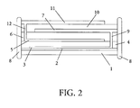
- Fig. 2 has the analog basic structure as described in Fig. 1 but additionally a third dielectric layer 10 and a third electrode 11
- Dielectric layer 10 has a dielectric constant of K> 3 and can be the same Contain materials such as the dielectric layer 6.
- the third electrode 11 contains same materials as the second electrode 7.
- the third electrode 11 is via a via 12 through the dielectric layers 6 and 10 with the first electrode 5 by means of, for example Aluminum, aluminum doped with copper, copper, platinum or nickel.
Landscapes
- Fixed Capacitors And Capacitor Manufacturing Machines (AREA)
- Ceramic Capacitors (AREA)
- Structures For Mounting Electric Components On Printed Circuit Boards (AREA)
- Semiconductor Integrated Circuits (AREA)
Applications Claiming Priority (2)
| Application Number | Priority Date | Filing Date | Title |
|---|---|---|---|
| DE19903456 | 1999-01-28 | ||
| DE19903456A DE19903456A1 (de) | 1999-01-28 | 1999-01-28 | Mehrkomponenten-Bauteil |
Publications (3)
| Publication Number | Publication Date |
|---|---|
| EP1024593A2 true EP1024593A2 (fr) | 2000-08-02 |
| EP1024593A3 EP1024593A3 (fr) | 2003-12-10 |
| EP1024593B1 EP1024593B1 (fr) | 2007-02-21 |
Family
ID=7895722
Family Applications (1)
| Application Number | Title | Priority Date | Filing Date |
|---|---|---|---|
| EP00200236A Expired - Lifetime EP1024593B1 (fr) | 1999-01-28 | 2000-01-21 | Composant à plusieurs éléments |
Country Status (4)
| Country | Link |
|---|---|
| US (1) | US6507498B1 (fr) |
| EP (1) | EP1024593B1 (fr) |
| JP (1) | JP2000223379A (fr) |
| DE (2) | DE19903456A1 (fr) |
Cited By (1)
| Publication number | Priority date | Publication date | Assignee | Title |
|---|---|---|---|---|
| WO2007014550A1 (fr) * | 2005-08-01 | 2007-02-08 | Epcos Ag | Composant electrique |
Families Citing this family (4)
| Publication number | Priority date | Publication date | Assignee | Title |
|---|---|---|---|---|
| US6780494B2 (en) * | 2002-03-07 | 2004-08-24 | Tdk Corporation | Ceramic electronic device and method of production of same |
| JP4654854B2 (ja) * | 2005-09-13 | 2011-03-23 | パナソニック株式会社 | 積層コンデンサ及びモールドコンデンサ |
| KR101514562B1 (ko) * | 2013-11-06 | 2015-04-22 | 삼성전기주식회사 | 적층 세라믹 전자 부품 및 그 실장 기판 |
| US10381161B2 (en) * | 2017-11-06 | 2019-08-13 | Advanced Semiconductor Engineering, Inc. | Capacitor structure |
Family Cites Families (8)
| Publication number | Priority date | Publication date | Assignee | Title |
|---|---|---|---|---|
| ATE35344T1 (de) * | 1985-01-17 | 1988-07-15 | Siemens Bauelemente Ohg | Spannungsabhaengiger elektrischer widerstand (varistor). |
| US4714981A (en) * | 1986-04-09 | 1987-12-22 | Rca Corporation | Cover for a semiconductor package |
| JPS62265796A (ja) * | 1986-05-14 | 1987-11-18 | 株式会社住友金属セラミックス | セラミツク多層配線基板およびその製造法 |
| JP2790640B2 (ja) * | 1989-01-14 | 1998-08-27 | ティーディーケイ株式会社 | 混成集積回路部品の構造 |
| JPH03203212A (ja) * | 1989-12-28 | 1991-09-04 | Nippon Chemicon Corp | 複合チップ部品及びその製造方法 |
| US5548474A (en) * | 1994-03-01 | 1996-08-20 | Avx Corporation | Electrical components such as capacitors having electrodes with an insulating edge |
| US5576925A (en) * | 1994-12-27 | 1996-11-19 | General Electric Company | Flexible multilayer thin film capacitors |
| US5889445A (en) * | 1997-07-22 | 1999-03-30 | Avx Corporation | Multilayer ceramic RC device |
-
1999
- 1999-01-28 DE DE19903456A patent/DE19903456A1/de not_active Withdrawn
-
2000
- 2000-01-21 EP EP00200236A patent/EP1024593B1/fr not_active Expired - Lifetime
- 2000-01-21 DE DE50014073T patent/DE50014073D1/de not_active Expired - Lifetime
- 2000-01-26 JP JP2000016722A patent/JP2000223379A/ja not_active Withdrawn
- 2000-01-26 US US09/491,626 patent/US6507498B1/en not_active Expired - Lifetime
Cited By (1)
| Publication number | Priority date | Publication date | Assignee | Title |
|---|---|---|---|---|
| WO2007014550A1 (fr) * | 2005-08-01 | 2007-02-08 | Epcos Ag | Composant electrique |
Also Published As
| Publication number | Publication date |
|---|---|
| JP2000223379A (ja) | 2000-08-11 |
| EP1024593A3 (fr) | 2003-12-10 |
| DE50014073D1 (de) | 2007-04-05 |
| US6507498B1 (en) | 2003-01-14 |
| DE19903456A1 (de) | 2000-08-10 |
| EP1024593B1 (fr) | 2007-02-21 |
Similar Documents
| Publication | Publication Date | Title |
|---|---|---|
| EP2174328B1 (fr) | Composant multicouche électrique avec une résistance et une couche de découplage | |
| EP1606831B1 (fr) | Composant multicouche electrique | |
| DE19915247A1 (de) | Spannungsabhängiger Dünnschichtkondensator | |
| EP1022768A2 (fr) | Condensateur à couche mince résistant à la tension avec structure interdigitale | |
| DE102006000935B4 (de) | Monolithisches keramisches Bauelement und Verfahren zur Herstellung | |
| DE19903500A1 (de) | Dünnschichtschaltkreis mit Bauteil | |
| EP1369880B1 (fr) | Composant électrique multicouche et circuit | |
| DE112020002054T5 (de) | Integrierte komponente, einen kondensator und einen eigenständigen varistor aufweisend | |
| DE112021006219T5 (de) | Mehrschichtiger Keramikkondensator | |
| EP2517218B1 (fr) | Varactor et sa methode de fabrication | |
| DE112018005239T5 (de) | Abstimmbarer Mehrschichtkondensator mit hoher Kapazität und Array | |
| EP2396795A1 (fr) | Composant électronique céramique à couches multiples et son procédé de fabrication | |
| EP1024593B1 (fr) | Composant à plusieurs éléments | |
| DE102004016146B4 (de) | Elektrisches Vielschichtbauelement | |
| DE102020118857B4 (de) | Vielschichtkondensator | |
| DE10026258B4 (de) | Keramisches Material, keramisches Bauelement mit dem keramischen Material und Verwendung des keramischen Bauelements | |
| EP1022769A2 (fr) | Composant passif ceramique | |
| DE19651554C2 (de) | Halbleiterbauelement, das gegen elektromagnetische Störungen geschützt ist | |
| DE112023004557T5 (de) | Mehrschichtiger Kondensator | |
| DE19902865A1 (de) | Zero-IF-Konverter mit RC-Filter | |
| DE10231209B4 (de) | Piezoelektrisches Bauelement | |
| DE69735378T2 (de) | Verfahren zur herstellung eines bauelements mit mehrfacher schutzfunktion | |
| DE112021006016T5 (de) | System und Verfahren zum Mischen von Radiofrequenzsignalen | |
| EP1911052B1 (fr) | Composant electrique | |
| DE10134751C1 (de) | Elektrokeramisches Bauelement |
Legal Events
| Date | Code | Title | Description |
|---|---|---|---|
| PUAI | Public reference made under article 153(3) epc to a published international application that has entered the european phase |
Free format text: ORIGINAL CODE: 0009012 |
|
| AK | Designated contracting states |
Kind code of ref document: A2 Designated state(s): AT BE CH CY DE DK ES FI FR GB GR IE IT LI LU MC NL PT SE |
|
| AX | Request for extension of the european patent |
Free format text: AL;LT;LV;MK;RO;SI |
|
| RAP1 | Party data changed (applicant data changed or rights of an application transferred) |
Owner name: PHILIPS CORPORATE INTELLECTUAL PROPERTY GMBH Owner name: KONINKLIJKE PHILIPS ELECTRONICS N.V. |
|
| RAP1 | Party data changed (applicant data changed or rights of an application transferred) |
Owner name: PHILIPS INTELLECTUAL PROPERTY & STANDARDS GMBH Owner name: KONINKLIJKE PHILIPS ELECTRONICS N.V. |
|
| PUAL | Search report despatched |
Free format text: ORIGINAL CODE: 0009013 |
|
| AK | Designated contracting states |
Kind code of ref document: A3 Designated state(s): AT BE CH CY DE DK ES FI FR GB GR IE IT LI LU MC NL PT SE |
|
| AX | Request for extension of the european patent |
Extension state: AL LT LV MK RO SI |
|
| 17P | Request for examination filed |
Effective date: 20040611 |
|
| AKX | Designation fees paid |
Designated state(s): DE FR GB |
|
| GRAP | Despatch of communication of intention to grant a patent |
Free format text: ORIGINAL CODE: EPIDOSNIGR1 |
|
| GRAS | Grant fee paid |
Free format text: ORIGINAL CODE: EPIDOSNIGR3 |
|
| GRAA | (expected) grant |
Free format text: ORIGINAL CODE: 0009210 |
|
| AK | Designated contracting states |
Kind code of ref document: B1 Designated state(s): DE FR GB |
|
| REG | Reference to a national code |
Ref country code: GB Ref legal event code: FG4D Free format text: NOT ENGLISH |
|
| REF | Corresponds to: |
Ref document number: 50014073 Country of ref document: DE Date of ref document: 20070405 Kind code of ref document: P |
|
| GBT | Gb: translation of ep patent filed (gb section 77(6)(a)/1977) |
Effective date: 20070516 |
|
| ET | Fr: translation filed | ||
| PLBE | No opposition filed within time limit |
Free format text: ORIGINAL CODE: 0009261 |
|
| STAA | Information on the status of an ep patent application or granted ep patent |
Free format text: STATUS: NO OPPOSITION FILED WITHIN TIME LIMIT |
|
| 26N | No opposition filed |
Effective date: 20071122 |
|
| REG | Reference to a national code |
Ref country code: GB Ref legal event code: 732E |
|
| REG | Reference to a national code |
Ref country code: FR Ref legal event code: TP |
|
| PGFP | Annual fee paid to national office [announced via postgrant information from national office to epo] |
Ref country code: GB Payment date: 20110119 Year of fee payment: 12 |
|
| PGFP | Annual fee paid to national office [announced via postgrant information from national office to epo] |
Ref country code: FR Payment date: 20120216 Year of fee payment: 13 |
|
| PGFP | Annual fee paid to national office [announced via postgrant information from national office to epo] |
Ref country code: DE Payment date: 20121226 Year of fee payment: 14 |
|
| GBPC | Gb: european patent ceased through non-payment of renewal fee |
Effective date: 20130121 |
|
| REG | Reference to a national code |
Ref country code: FR Ref legal event code: ST Effective date: 20130930 |
|
| PG25 | Lapsed in a contracting state [announced via postgrant information from national office to epo] |
Ref country code: GB Free format text: LAPSE BECAUSE OF NON-PAYMENT OF DUE FEES Effective date: 20130121 Ref country code: FR Free format text: LAPSE BECAUSE OF NON-PAYMENT OF DUE FEES Effective date: 20130131 |
|
| REG | Reference to a national code |
Ref country code: DE Ref legal event code: R119 Ref document number: 50014073 Country of ref document: DE |
|
| REG | Reference to a national code |
Ref country code: DE Ref legal event code: R119 Ref document number: 50014073 Country of ref document: DE Effective date: 20140801 |
|
| PG25 | Lapsed in a contracting state [announced via postgrant information from national office to epo] |
Ref country code: DE Free format text: LAPSE BECAUSE OF NON-PAYMENT OF DUE FEES Effective date: 20140801 |