EP1023632B1 - Verfahren und vorrichtung zum spektralen pegelabgleich in wdm vielkanalsystemen - Google Patents
Verfahren und vorrichtung zum spektralen pegelabgleich in wdm vielkanalsystemen Download PDFInfo
- Publication number
- EP1023632B1 EP1023632B1 EP98950097A EP98950097A EP1023632B1 EP 1023632 B1 EP1023632 B1 EP 1023632B1 EP 98950097 A EP98950097 A EP 98950097A EP 98950097 A EP98950097 A EP 98950097A EP 1023632 B1 EP1023632 B1 EP 1023632B1
- Authority
- EP
- European Patent Office
- Prior art keywords
- channels
- fibre
- spectral
- wdm
- oaslm
- Prior art date
- Legal status (The legal status is an assumption and is not a legal conclusion. Google has not performed a legal analysis and makes no representation as to the accuracy of the status listed.)
- Expired - Lifetime
Links
Images


Classifications
-
- G—PHYSICS
- G02—OPTICS
- G02B—OPTICAL ELEMENTS, SYSTEMS OR APPARATUS
- G02B6/00—Light guides; Structural details of arrangements comprising light guides and other optical elements, e.g. couplings
- G02B6/24—Coupling light guides
- G02B6/26—Optical coupling means
- G02B6/28—Optical coupling means having data bus means, i.e. plural waveguides interconnected and providing an inherently bidirectional system by mixing and splitting signals
- G02B6/293—Optical coupling means having data bus means, i.e. plural waveguides interconnected and providing an inherently bidirectional system by mixing and splitting signals with wavelength selective means
- G02B6/29379—Optical coupling means having data bus means, i.e. plural waveguides interconnected and providing an inherently bidirectional system by mixing and splitting signals with wavelength selective means characterised by the function or use of the complete device
- G02B6/29391—Power equalisation of different channels, e.g. power flattening
-
- G—PHYSICS
- G02—OPTICS
- G02B—OPTICAL ELEMENTS, SYSTEMS OR APPARATUS
- G02B6/00—Light guides; Structural details of arrangements comprising light guides and other optical elements, e.g. couplings
- G02B6/24—Coupling light guides
- G02B6/26—Optical coupling means
- G02B6/28—Optical coupling means having data bus means, i.e. plural waveguides interconnected and providing an inherently bidirectional system by mixing and splitting signals
- G02B6/293—Optical coupling means having data bus means, i.e. plural waveguides interconnected and providing an inherently bidirectional system by mixing and splitting signals with wavelength selective means
- G02B6/29304—Optical coupling means having data bus means, i.e. plural waveguides interconnected and providing an inherently bidirectional system by mixing and splitting signals with wavelength selective means operating by diffraction, e.g. grating
- G02B6/29305—Optical coupling means having data bus means, i.e. plural waveguides interconnected and providing an inherently bidirectional system by mixing and splitting signals with wavelength selective means operating by diffraction, e.g. grating as bulk element, i.e. free space arrangement external to a light guide
- G02B6/29308—Diffractive element having focusing properties, e.g. curved gratings
-
- G—PHYSICS
- G02—OPTICS
- G02B—OPTICAL ELEMENTS, SYSTEMS OR APPARATUS
- G02B6/00—Light guides; Structural details of arrangements comprising light guides and other optical elements, e.g. couplings
- G02B6/24—Coupling light guides
- G02B6/26—Optical coupling means
- G02B6/28—Optical coupling means having data bus means, i.e. plural waveguides interconnected and providing an inherently bidirectional system by mixing and splitting signals
- G02B6/293—Optical coupling means having data bus means, i.e. plural waveguides interconnected and providing an inherently bidirectional system by mixing and splitting signals with wavelength selective means
- G02B6/29304—Optical coupling means having data bus means, i.e. plural waveguides interconnected and providing an inherently bidirectional system by mixing and splitting signals with wavelength selective means operating by diffraction, e.g. grating
- G02B6/29305—Optical coupling means having data bus means, i.e. plural waveguides interconnected and providing an inherently bidirectional system by mixing and splitting signals with wavelength selective means operating by diffraction, e.g. grating as bulk element, i.e. free space arrangement external to a light guide
- G02B6/2931—Diffractive element operating in reflection
-
- G—PHYSICS
- G02—OPTICS
- G02B—OPTICAL ELEMENTS, SYSTEMS OR APPARATUS
- G02B6/00—Light guides; Structural details of arrangements comprising light guides and other optical elements, e.g. couplings
- G02B6/24—Coupling light guides
- G02B6/26—Optical coupling means
- G02B6/28—Optical coupling means having data bus means, i.e. plural waveguides interconnected and providing an inherently bidirectional system by mixing and splitting signals
- G02B6/293—Optical coupling means having data bus means, i.e. plural waveguides interconnected and providing an inherently bidirectional system by mixing and splitting signals with wavelength selective means
- G02B6/29304—Optical coupling means having data bus means, i.e. plural waveguides interconnected and providing an inherently bidirectional system by mixing and splitting signals with wavelength selective means operating by diffraction, e.g. grating
- G02B6/29316—Light guides comprising a diffractive element, e.g. grating in or on the light guide such that diffracted light is confined in the light guide
- G02B6/29317—Light guides of the optical fibre type
-
- G—PHYSICS
- G02—OPTICS
- G02B—OPTICAL ELEMENTS, SYSTEMS OR APPARATUS
- G02B6/00—Light guides; Structural details of arrangements comprising light guides and other optical elements, e.g. couplings
- G02B6/24—Coupling light guides
- G02B6/26—Optical coupling means
- G02B6/28—Optical coupling means having data bus means, i.e. plural waveguides interconnected and providing an inherently bidirectional system by mixing and splitting signals
- G02B6/293—Optical coupling means having data bus means, i.e. plural waveguides interconnected and providing an inherently bidirectional system by mixing and splitting signals with wavelength selective means
- G02B6/29304—Optical coupling means having data bus means, i.e. plural waveguides interconnected and providing an inherently bidirectional system by mixing and splitting signals with wavelength selective means operating by diffraction, e.g. grating
- G02B6/29316—Light guides comprising a diffractive element, e.g. grating in or on the light guide such that diffracted light is confined in the light guide
- G02B6/29323—Coupling to or out of the diffractive element through the lateral surface of the light guide
-
- G—PHYSICS
- G02—OPTICS
- G02F—OPTICAL DEVICES OR ARRANGEMENTS FOR THE CONTROL OF LIGHT BY MODIFICATION OF THE OPTICAL PROPERTIES OF THE MEDIA OF THE ELEMENTS INVOLVED THEREIN; NON-LINEAR OPTICS; FREQUENCY-CHANGING OF LIGHT; OPTICAL LOGIC ELEMENTS; OPTICAL ANALOGUE/DIGITAL CONVERTERS
- G02F1/00—Devices or arrangements for the control of the intensity, colour, phase, polarisation or direction of light arriving from an independent light source, e.g. switching, gating or modulating; Non-linear optics
- G02F1/01—Devices or arrangements for the control of the intensity, colour, phase, polarisation or direction of light arriving from an independent light source, e.g. switching, gating or modulating; Non-linear optics for the control of the intensity, phase, polarisation or colour
- G02F1/13—Devices or arrangements for the control of the intensity, colour, phase, polarisation or direction of light arriving from an independent light source, e.g. switching, gating or modulating; Non-linear optics for the control of the intensity, phase, polarisation or colour based on liquid crystals, e.g. single liquid crystal display cells
- G02F1/133—Constructional arrangements; Operation of liquid crystal cells; Circuit arrangements
- G02F1/1333—Constructional arrangements; Manufacturing methods
- G02F1/13338—Input devices, e.g. touch panels
-
- H—ELECTRICITY
- H04—ELECTRIC COMMUNICATION TECHNIQUE
- H04J—MULTIPLEX COMMUNICATION
- H04J14/00—Optical multiplex systems
- H04J14/02—Wavelength-division multiplex systems
- H04J14/0221—Power control, e.g. to keep the total optical power constant
-
- G—PHYSICS
- G02—OPTICS
- G02B—OPTICAL ELEMENTS, SYSTEMS OR APPARATUS
- G02B6/00—Light guides; Structural details of arrangements comprising light guides and other optical elements, e.g. couplings
- G02B6/24—Coupling light guides
- G02B6/26—Optical coupling means
- G02B6/28—Optical coupling means having data bus means, i.e. plural waveguides interconnected and providing an inherently bidirectional system by mixing and splitting signals
- G02B6/293—Optical coupling means having data bus means, i.e. plural waveguides interconnected and providing an inherently bidirectional system by mixing and splitting signals with wavelength selective means
- G02B6/29379—Optical coupling means having data bus means, i.e. plural waveguides interconnected and providing an inherently bidirectional system by mixing and splitting signals with wavelength selective means characterised by the function or use of the complete device
- G02B6/29395—Optical coupling means having data bus means, i.e. plural waveguides interconnected and providing an inherently bidirectional system by mixing and splitting signals with wavelength selective means characterised by the function or use of the complete device configurable, e.g. tunable or reconfigurable
Landscapes
- Physics & Mathematics (AREA)
- Optics & Photonics (AREA)
- General Physics & Mathematics (AREA)
- Nonlinear Science (AREA)
- Crystallography & Structural Chemistry (AREA)
- Chemical & Material Sciences (AREA)
- Mathematical Physics (AREA)
- Engineering & Computer Science (AREA)
- Computer Networks & Wireless Communication (AREA)
- Signal Processing (AREA)
- Optical Modulation, Optical Deflection, Nonlinear Optics, Optical Demodulation, Optical Logic Elements (AREA)
- Optical Couplings Of Light Guides (AREA)
- Liquid Crystal (AREA)
- Mobile Radio Communication Systems (AREA)
- Optical Communication System (AREA)
Description

Claims (4)
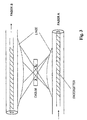
- Verfahren zum spektralen Pegelabgleich in WDM Vielkanalsystemen unter Verwendung selektiver Lichtabschwächer, in die Licht aus einer Faser über spektral aufspaltende und abbildende Elemente projiziert wird, dadurch gekennzeichnet, daßdas Licht aus der Faser nach spektraler Aufspaltung in Kanäle örtlich getrennt auf die Oberfläche eines optischen Begrenzers auf der Basis eines optisch adressierbaren Lichtventils, OASLM, projiziert wird,daß darin die Kanäle mit gegenüber anderen Kanälen höherem Pegel mehr als die anderen Kanäle geschwächt werden, indem die nichtlineare Transmissionscharakteristik des optisch adressierbaren Lichtventils, OASLM, zur Nivellierung der WDM Kanäle ausgenutzt wird, unddaß zuletzt die Kanäle wieder auf einen Punkt abgebildet und in eine weitere Faser eingekoppelt werden.
- Vorrichtung zum spektralen Pegelabgleich in WDM Vielkanalsystemen, welche, unter Verwendung selektiver Lichtabschwächer, das Licht aus einer Faser über spektral aufspaltende und abbildende Elemente in eine weitere Faser projiziert,
dadurch gekennzeichnet, daß
sie aus in bzw. an eine Faser (A) ein- bzw. angebauten spektral aufspaltenden Elementen, einem selektiven Lichtabschwächer auf der Basis eines optisch adressierbaren Lichtventils, OASLM, und einer weiteren Faser (B) mit ebenso ein-bzw. angebauten spektral aufspaltenden Elementen besteht, wobei das optisch adressierbare Licht ventil auf der Projektions fläche Zwischen den Spektral aufspaltenden und abbildenden Elementen angeordnet ist, so dass darin die örtlich getrennten Spektralen Kanäle mit gegenüber anderen Kanälen höherem Pegel mehr als die anderen Kanäle geschwächt werden, in dem die nichtlineare Transmissionscharakteristik des optisch adressierbaren Licht ventils zum Pegelausgleich ausgenutzt ist. - Vorrichtung nach Anspruch 2 dadurch gekennzeichnet, daß als an die Fasern (A;B) angebaute, spektral aufspaltende und abbildende Elemente gewölbte Gitter angeordnet sind.
- Vorrichtung nach Anspruch 2 dadurch gekennzeichnet, daß die in die Fasern (A;B) eingebauten, spektral aufspaltenden Elemente Fasergitter sind, die mit anamorphotischen Linsen auf der Faser zur Abbildung ausgestattet sind.
Applications Claiming Priority (3)
| Application Number | Priority Date | Filing Date | Title |
|---|---|---|---|
| DE19745323 | 1997-10-14 | ||
| DE19745323A DE19745323C2 (de) | 1997-10-14 | 1997-10-14 | Verfahren und Vorrichtung zum spektralen Pegelableich in MDW Vielkanalsystemen |
| PCT/EP1998/006208 WO1999019768A1 (de) | 1997-10-14 | 1998-09-30 | Verfahren und vorrichtung zum spektralen pegelabgleich in wdm vielkanalsystemen |
Publications (2)
| Publication Number | Publication Date |
|---|---|
| EP1023632A1 EP1023632A1 (de) | 2000-08-02 |
| EP1023632B1 true EP1023632B1 (de) | 2001-12-05 |
Family
ID=7845492
Family Applications (1)
| Application Number | Title | Priority Date | Filing Date |
|---|---|---|---|
| EP98950097A Expired - Lifetime EP1023632B1 (de) | 1997-10-14 | 1998-09-30 | Verfahren und vorrichtung zum spektralen pegelabgleich in wdm vielkanalsystemen |
Country Status (5)
| Country | Link |
|---|---|
| US (2) | US6563980B1 (de) |
| EP (1) | EP1023632B1 (de) |
| AT (1) | ATE210310T1 (de) |
| DE (2) | DE19745323C2 (de) |
| WO (1) | WO1999019768A1 (de) |
Families Citing this family (3)
| Publication number | Priority date | Publication date | Assignee | Title |
|---|---|---|---|---|
| DE19745323C2 (de) * | 1997-10-14 | 1999-09-16 | Deutsche Telekom Ag | Verfahren und Vorrichtung zum spektralen Pegelableich in MDW Vielkanalsystemen |
| DE10043985A1 (de) | 2000-09-05 | 2002-03-14 | Cube Optics Ag | Optischer Modifizierer und Verfahren zur Herstellung hierfür |
| SE519224C2 (sv) * | 2000-12-29 | 2003-02-04 | Proximion Fiber Optics Ab | Optiskt arrangemang |
Family Cites Families (16)
| Publication number | Priority date | Publication date | Assignee | Title |
|---|---|---|---|---|
| DE3148427A1 (de) * | 1981-12-08 | 1983-06-16 | Messerschmitt-Bölkow-Blohm GmbH, 8000 München | Ortsabhaengig modulierbarer interferenzfilter |
| DE3929480A1 (de) * | 1989-09-05 | 1991-03-07 | Siemens Ag | Anordnung zum (de)multiplexen von lichtwellen unterschiedlicher wellenlaenge |
| US5007705A (en) * | 1989-12-26 | 1991-04-16 | United Technologies Corporation | Variable optical fiber Bragg filter arrangement |
| US5042897A (en) * | 1989-12-26 | 1991-08-27 | United Technologies Corporation | Optical waveguide embedded light redirecting Bragg grating arrangement |
| GB9005647D0 (en) * | 1990-03-13 | 1990-05-09 | Secr Defence | Optical multiplexer |
| US5351317A (en) * | 1992-08-14 | 1994-09-27 | Telefonaktiebolaget L M Ericsson | Interferometric tunable optical filter |
| DE4326522A1 (de) * | 1993-08-06 | 1995-02-09 | Siemens Ag | Programmierbares optisches Filter und optische Schaltanordnung |
| DE59310361D1 (de) * | 1993-10-29 | 2004-07-29 | Siemens Ag | Optisches, transparentes Ringnetz mit Auskoppelung eines Signales einer Wellenlänge in einem oder mehreren Ringknoten |
| US5541766A (en) | 1994-11-30 | 1996-07-30 | At&T Corp. | Gain control for optically amplified systems |
| FR2731280B1 (fr) * | 1995-03-03 | 1997-04-04 | Hamel Andre | Multiplexeur optique a insertion-extraction a haute isolation |
| US6093246A (en) * | 1995-09-08 | 2000-07-25 | Sandia Corporation | Photonic crystal devices formed by a charged-particle beam |
| KR0155521B1 (ko) * | 1995-12-20 | 1998-11-16 | 양승택 | 광통신용 패킷 어드레스 검출기 |
| JP3883601B2 (ja) * | 1996-03-27 | 2007-02-21 | 富士通株式会社 | 光イコライザ |
| US5699377A (en) * | 1996-04-30 | 1997-12-16 | E-Tek Dynamics, Inc. | Narrow linewidth, stabilized semiconductor laser source |
| US5832156A (en) * | 1996-10-31 | 1998-11-03 | Lucent Technologies Inc. | Article comprising an optical waveguide tap |
| DE19745323C2 (de) * | 1997-10-14 | 1999-09-16 | Deutsche Telekom Ag | Verfahren und Vorrichtung zum spektralen Pegelableich in MDW Vielkanalsystemen |
-
1997
- 1997-10-14 DE DE19745323A patent/DE19745323C2/de not_active Expired - Fee Related
-
1998
- 1998-09-30 AT AT98950097T patent/ATE210310T1/de active
- 1998-09-30 US US09/529,535 patent/US6563980B1/en not_active Expired - Fee Related
- 1998-09-30 WO PCT/EP1998/006208 patent/WO1999019768A1/de active IP Right Grant
- 1998-09-30 DE DE59802373T patent/DE59802373D1/de not_active Expired - Lifetime
- 1998-09-30 EP EP98950097A patent/EP1023632B1/de not_active Expired - Lifetime
-
2002
- 2002-09-12 US US10/243,174 patent/US20030031405A1/en not_active Abandoned
Also Published As
| Publication number | Publication date |
|---|---|
| ATE210310T1 (de) | 2001-12-15 |
| US6563980B1 (en) | 2003-05-13 |
| EP1023632A1 (de) | 2000-08-02 |
| DE19745323C2 (de) | 1999-09-16 |
| WO1999019768A1 (de) | 1999-04-22 |
| US20030031405A1 (en) | 2003-02-13 |
| DE19745323A1 (de) | 1999-05-06 |
| DE59802373D1 (de) | 2002-01-17 |
Similar Documents
| Publication | Publication Date | Title |
|---|---|---|
| DE69838707T2 (de) | Optische vorrichtung, die eine virtuell abgebildete phasenmatrix zur erzeugung von chromatischer dispersion verwendet | |
| DE69435053T2 (de) | Optische Faser für Wellenlängen-Multiplexer | |
| DE60200944T2 (de) | Gerät zur erzeugung einer taktfluktuationstoleranten optischen modulation eines ersten signals durch ein zweites signal | |
| DE69834004T2 (de) | Minimierung der Dispersion von faseroptischen Übertragungsstrecken | |
| DE69730553T2 (de) | Farbanzeigevorrichtung mit einer Flüssigkristallplatte und Brechungsgitter | |
| WO1996025009A1 (de) | Farbbilderzeugungssysteme und verwendungen | |
| Starodubov et al. | All-fiber bandpass filter with adjustable transmission using cladding-mode coupling | |
| WO1996024869A1 (de) | Verbindungsaufspalter aus streifen-wellenleitern und verwendungen | |
| DE112015000351T5 (de) | Anzeigevorrichtung für eine holografische Rekonstruktion | |
| DE2715311A1 (de) | Optische verbindungsvorrichtung | |
| DE2527939C2 (de) | Verfahren zum Betreiben eines ebenen Multimoden-Lichtwellenleiters | |
| DE60106520T2 (de) | Vorrichtung zum Regenerieren optischer Signale | |
| EP1023632B1 (de) | Verfahren und vorrichtung zum spektralen pegelabgleich in wdm vielkanalsystemen | |
| DE19911182C2 (de) | Faser-Transmissionsbauelement zur Erzeugung chromatischer Dispersion | |
| DE69823835T2 (de) | Faseroptisches übertragungssystem | |
| DE60214316T2 (de) | Chirp-Messverfahren | |
| DE602004012178T2 (de) | Verfahren und Vorrichtung zum Bereitstellen einer Mehrwellenlängen-Lichtquelle | |
| DE102009028984A1 (de) | Beleuchtungseinheit für ein Direktsichtdisplay | |
| DE112019000241T5 (de) | Spannungsoptisches Phasenschieberarray für Lidar und andere Anwendungen | |
| DE60114387T2 (de) | Einrichtung und verfahren zum optischen add/drop-multiplexen | |
| DE60208669T2 (de) | Optisches übertragungssystem mit einer optischen phasenkonjugationsvorrichtung | |
| DE19723208A1 (de) | Vorrichtung zum Intensitätsmodulieren eines Lichtbündels, ein Herstellungsverfahren für diese, ein Verfahren zum Intensitätsmodulieren eines Lichtbündels sowie Verwendungen von der Vorrichtung | |
| DE19503930A1 (de) | Verbindungsaufspalter aus Streifen-Wellenleitern und Verwendungen | |
| Taylor et al. | Responses of a spatial light modulator to pulsed electron irradiations | |
| DE3148427A1 (de) | Ortsabhaengig modulierbarer interferenzfilter |
Legal Events
| Date | Code | Title | Description |
|---|---|---|---|
| PUAI | Public reference made under article 153(3) epc to a published international application that has entered the european phase |
Free format text: ORIGINAL CODE: 0009012 |
|
| 17P | Request for examination filed |
Effective date: 20000515 |
|
| AK | Designated contracting states |
Kind code of ref document: A1 Designated state(s): AT BE CH CY DE DK ES FI FR GB GR IE IT LI LU MC NL PT SE |
|
| 17Q | First examination report despatched |
Effective date: 20000919 |
|
| GRAG | Despatch of communication of intention to grant |
Free format text: ORIGINAL CODE: EPIDOS AGRA |
|
| GRAG | Despatch of communication of intention to grant |
Free format text: ORIGINAL CODE: EPIDOS AGRA |
|
| GRAH | Despatch of communication of intention to grant a patent |
Free format text: ORIGINAL CODE: EPIDOS IGRA |
|
| GRAH | Despatch of communication of intention to grant a patent |
Free format text: ORIGINAL CODE: EPIDOS IGRA |
|
| GRAA | (expected) grant |
Free format text: ORIGINAL CODE: 0009210 |
|
| AK | Designated contracting states |
Kind code of ref document: B1 Designated state(s): AT BE CH CY DE DK ES FI FR GB GR IE IT LI LU MC NL PT SE |
|
| PG25 | Lapsed in a contracting state [announced via postgrant information from national office to epo] |
Ref country code: IE Free format text: LAPSE BECAUSE OF FAILURE TO SUBMIT A TRANSLATION OF THE DESCRIPTION OR TO PAY THE FEE WITHIN THE PRESCRIBED TIME-LIMIT Effective date: 20011205 Ref country code: GR Free format text: LAPSE BECAUSE OF FAILURE TO SUBMIT A TRANSLATION OF THE DESCRIPTION OR TO PAY THE FEE WITHIN THE PRESCRIBED TIME-LIMIT Effective date: 20011205 |
|
| REF | Corresponds to: |
Ref document number: 210310 Country of ref document: AT Date of ref document: 20011215 Kind code of ref document: T |
|
| REG | Reference to a national code |
Ref country code: CH Ref legal event code: NV Representative=s name: HUG INTERLIZENZ AG Ref country code: CH Ref legal event code: EP |
|
| REG | Reference to a national code |
Ref country code: GB Ref legal event code: IF02 |
|
| REG | Reference to a national code |
Ref country code: IE Ref legal event code: FG4D Free format text: GERMAN |
|
| REF | Corresponds to: |
Ref document number: 59802373 Country of ref document: DE Date of ref document: 20020117 |
|
| PG25 | Lapsed in a contracting state [announced via postgrant information from national office to epo] |
Ref country code: PT Free format text: LAPSE BECAUSE OF FAILURE TO SUBMIT A TRANSLATION OF THE DESCRIPTION OR TO PAY THE FEE WITHIN THE PRESCRIBED TIME-LIMIT Effective date: 20020305 Ref country code: DK Free format text: LAPSE BECAUSE OF FAILURE TO SUBMIT A TRANSLATION OF THE DESCRIPTION OR TO PAY THE FEE WITHIN THE PRESCRIBED TIME-LIMIT Effective date: 20020305 |
|
| GBT | Gb: translation of ep patent filed (gb section 77(6)(a)/1977) |
Effective date: 20020222 |
|
| ET | Fr: translation filed | ||
| PG25 | Lapsed in a contracting state [announced via postgrant information from national office to epo] |
Ref country code: ES Free format text: LAPSE BECAUSE OF FAILURE TO SUBMIT A TRANSLATION OF THE DESCRIPTION OR TO PAY THE FEE WITHIN THE PRESCRIBED TIME-LIMIT Effective date: 20020627 |
|
| REG | Reference to a national code |
Ref country code: IE Ref legal event code: FD4D |
|
| PG25 | Lapsed in a contracting state [announced via postgrant information from national office to epo] |
Ref country code: LU Free format text: LAPSE BECAUSE OF NON-PAYMENT OF DUE FEES Effective date: 20020930 Ref country code: CY Free format text: LAPSE BECAUSE OF FAILURE TO SUBMIT A TRANSLATION OF THE DESCRIPTION OR TO PAY THE FEE WITHIN THE PRESCRIBED TIME-LIMIT Effective date: 20020930 |
|
| PLBE | No opposition filed within time limit |
Free format text: ORIGINAL CODE: 0009261 |
|
| STAA | Information on the status of an ep patent application or granted ep patent |
Free format text: STATUS: NO OPPOSITION FILED WITHIN TIME LIMIT |
|
| 26N | No opposition filed | ||
| PG25 | Lapsed in a contracting state [announced via postgrant information from national office to epo] |
Ref country code: MC Free format text: LAPSE BECAUSE OF NON-PAYMENT OF DUE FEES Effective date: 20030401 |
|
| PGFP | Annual fee paid to national office [announced via postgrant information from national office to epo] |
Ref country code: CH Payment date: 20110926 Year of fee payment: 14 |
|
| PGFP | Annual fee paid to national office [announced via postgrant information from national office to epo] |
Ref country code: SE Payment date: 20120920 Year of fee payment: 15 Ref country code: FI Payment date: 20120919 Year of fee payment: 15 Ref country code: GB Payment date: 20120920 Year of fee payment: 15 |
|
| PGFP | Annual fee paid to national office [announced via postgrant information from national office to epo] |
Ref country code: IT Payment date: 20120925 Year of fee payment: 15 |
|
| PGFP | Annual fee paid to national office [announced via postgrant information from national office to epo] |
Ref country code: NL Payment date: 20120920 Year of fee payment: 15 Ref country code: BE Payment date: 20120919 Year of fee payment: 15 Ref country code: DE Payment date: 20121126 Year of fee payment: 15 Ref country code: FR Payment date: 20121008 Year of fee payment: 15 |
|
| PGFP | Annual fee paid to national office [announced via postgrant information from national office to epo] |
Ref country code: AT Payment date: 20120919 Year of fee payment: 15 |
|
| BERE | Be: lapsed |
Owner name: DEUTSCHE *TELEKOM A.G. Effective date: 20130930 |
|
| REG | Reference to a national code |
Ref country code: NL Ref legal event code: V1 Effective date: 20140401 |
|
| PG25 | Lapsed in a contracting state [announced via postgrant information from national office to epo] |
Ref country code: FI Free format text: LAPSE BECAUSE OF NON-PAYMENT OF DUE FEES Effective date: 20130930 |
|
| REG | Reference to a national code |
Ref country code: CH Ref legal event code: PL |
|
| REG | Reference to a national code |
Ref country code: AT Ref legal event code: MM01 Ref document number: 210310 Country of ref document: AT Kind code of ref document: T Effective date: 20130930 |
|
| GBPC | Gb: european patent ceased through non-payment of renewal fee |
Effective date: 20130930 |
|
| REG | Reference to a national code |
Ref country code: SE Ref legal event code: EUG |
|
| REG | Reference to a national code |
Ref country code: DE Ref legal event code: R119 Ref document number: 59802373 Country of ref document: DE Effective date: 20140401 |
|
| REG | Reference to a national code |
Ref country code: FR Ref legal event code: ST Effective date: 20140530 |
|
| PG25 | Lapsed in a contracting state [announced via postgrant information from national office to epo] |
Ref country code: GB Free format text: LAPSE BECAUSE OF NON-PAYMENT OF DUE FEES Effective date: 20130930 Ref country code: CH Free format text: LAPSE BECAUSE OF NON-PAYMENT OF DUE FEES Effective date: 20130930 Ref country code: LI Free format text: LAPSE BECAUSE OF NON-PAYMENT OF DUE FEES Effective date: 20130930 Ref country code: BE Free format text: LAPSE BECAUSE OF NON-PAYMENT OF DUE FEES Effective date: 20130930 |
|
| PG25 | Lapsed in a contracting state [announced via postgrant information from national office to epo] |
Ref country code: SE Free format text: LAPSE BECAUSE OF NON-PAYMENT OF DUE FEES Effective date: 20131001 Ref country code: IT Free format text: LAPSE BECAUSE OF NON-PAYMENT OF DUE FEES Effective date: 20130930 Ref country code: FR Free format text: LAPSE BECAUSE OF NON-PAYMENT OF DUE FEES Effective date: 20130930 Ref country code: DE Free format text: LAPSE BECAUSE OF NON-PAYMENT OF DUE FEES Effective date: 20140401 Ref country code: AT Free format text: LAPSE BECAUSE OF NON-PAYMENT OF DUE FEES Effective date: 20130930 Ref country code: NL Free format text: LAPSE BECAUSE OF NON-PAYMENT OF DUE FEES Effective date: 20140401 |