EP1020814A2 - Process for producing non-contact data carrier - Google Patents
Process for producing non-contact data carrier Download PDFInfo
- Publication number
- EP1020814A2 EP1020814A2 EP00100051A EP00100051A EP1020814A2 EP 1020814 A2 EP1020814 A2 EP 1020814A2 EP 00100051 A EP00100051 A EP 00100051A EP 00100051 A EP00100051 A EP 00100051A EP 1020814 A2 EP1020814 A2 EP 1020814A2
- Authority
- EP
- European Patent Office
- Prior art keywords
- photo
- resin composition
- curable resin
- data carrier
- contact data
- Prior art date
- Legal status (The legal status is an assumption and is not a legal conclusion. Google has not performed a legal analysis and makes no representation as to the accuracy of the status listed.)
- Withdrawn
Links
Images


Classifications
-
- G—PHYSICS
- G06—COMPUTING OR CALCULATING; COUNTING
- G06K—GRAPHICAL DATA READING; PRESENTATION OF DATA; RECORD CARRIERS; HANDLING RECORD CARRIERS
- G06K19/00—Record carriers for use with machines and with at least a part designed to carry digital markings
- G06K19/06—Record carriers for use with machines and with at least a part designed to carry digital markings characterised by the kind of the digital marking, e.g. shape, nature, code
- G06K19/067—Record carriers with conductive marks, printed circuits or semiconductor circuit elements, e.g. credit or identity cards also with resonating or responding marks without active components
- G06K19/07—Record carriers with conductive marks, printed circuits or semiconductor circuit elements, e.g. credit or identity cards also with resonating or responding marks without active components with integrated circuit chips
- G06K19/077—Constructional details, e.g. mounting of circuits in the carrier
- G06K19/07745—Mounting details of integrated circuit chips
-
- G—PHYSICS
- G06—COMPUTING OR CALCULATING; COUNTING
- G06K—GRAPHICAL DATA READING; PRESENTATION OF DATA; RECORD CARRIERS; HANDLING RECORD CARRIERS
- G06K19/00—Record carriers for use with machines and with at least a part designed to carry digital markings
- G06K19/04—Record carriers for use with machines and with at least a part designed to carry digital markings characterised by the shape
-
- G—PHYSICS
- G06—COMPUTING OR CALCULATING; COUNTING
- G06K—GRAPHICAL DATA READING; PRESENTATION OF DATA; RECORD CARRIERS; HANDLING RECORD CARRIERS
- G06K19/00—Record carriers for use with machines and with at least a part designed to carry digital markings
- G06K19/06—Record carriers for use with machines and with at least a part designed to carry digital markings characterised by the kind of the digital marking, e.g. shape, nature, code
- G06K19/067—Record carriers with conductive marks, printed circuits or semiconductor circuit elements, e.g. credit or identity cards also with resonating or responding marks without active components
- G06K19/07—Record carriers with conductive marks, printed circuits or semiconductor circuit elements, e.g. credit or identity cards also with resonating or responding marks without active components with integrated circuit chips
- G06K19/077—Constructional details, e.g. mounting of circuits in the carrier
- G06K19/07749—Constructional details, e.g. mounting of circuits in the carrier the record carrier being capable of non-contact communication, e.g. constructional details of the antenna of a non-contact smart card
-
- H—ELECTRICITY
- H05—ELECTRIC TECHNIQUES NOT OTHERWISE PROVIDED FOR
- H05K—PRINTED CIRCUITS; CASINGS OR CONSTRUCTIONAL DETAILS OF ELECTRIC APPARATUS; MANUFACTURE OF ASSEMBLAGES OF ELECTRICAL COMPONENTS
- H05K3/00—Apparatus or processes for manufacturing printed circuits
- H05K3/22—Secondary treatment of printed circuits
- H05K3/28—Applying non-metallic protective coatings
- H05K3/281—Applying non-metallic protective coatings by means of a preformed insulating foil
-
- H—ELECTRICITY
- H05—ELECTRIC TECHNIQUES NOT OTHERWISE PROVIDED FOR
- H05K—PRINTED CIRCUITS; CASINGS OR CONSTRUCTIONAL DETAILS OF ELECTRIC APPARATUS; MANUFACTURE OF ASSEMBLAGES OF ELECTRICAL COMPONENTS
- H05K3/00—Apparatus or processes for manufacturing printed circuits
- H05K3/22—Secondary treatment of printed circuits
- H05K3/28—Applying non-metallic protective coatings
- H05K3/284—Applying non-metallic protective coatings for encapsulating mounted components
Definitions
- the present invention relates to a process for producing a non-contact data carrier or a radio frequency identification card.
- the process of the present invention is suitable for producing a thin resin-sealed non-contact data carrier.
- a non-contact data carrier system is now in general use. This system includes a data carrier and an interrogator, and a data transmission is made without contact therebetween.
- the non-contact data carrier system is applied to, for example, commuting tickets of various transportation facilities, or for entrance and exit controls in various facilities or companies.
- a resin-sealed non-contact data carrier is generally used. This has brought about a further miniaturization of the device and in particular a thinner device.
- a resin-sealed non-contact data carrier is produced by forming a non-contact data carrier element generally containing an antenna circuit, an IC chip, and optionally, other electronic components such as a condenser or a battery, on one side of a substrate film, and sealing the non-contact data carrier element with a thermoplastic resin or a thermosetting resin.
- the non-contact data carrier element must not be broken, and a surface of the sealed-resin layer must not be affected by an irregular or uneven structure formed from a combination of a flat substrate film and the non-contact data carrier element mounted thereon.
- voids may cause cracking or peeling. If the resin is forced into the depressed portions, there occurs a risk of breaking the non-contact data carrier element.
- the sealed resin layer When a thermoplastic resin is used as the sealing resin, the sealed resin layer must be thicker, to ensure that the surface of the sealed resin layer is not affected by the irregular or uneven structure derived from the non-contact data carrier element. Therefore, a thermoplastic resin is not suitable for obtaining a thinner non-contact data carrier. Further, when a thermosetting resin is used as the sealing resin, it is necessary to apply heat upon curing, and therefore, a material having a low thermal resistance cannot be used. Further, in a non-contact data carrier containing a built-in battery, a liquid leakage from or a bursting of the battery may sometimes occur.
- the object of the present invention is to provide a process which enables the production of a thin non-contact data carrier; without a breakage of the non-contact data carrier element upon the coating or sealing thereof with a resin; without an affect on the surface of the sealed resin layer by an irregular or uneven structure formed from a combination of the flat substrate film and the non-contact data carrier element mounted thereon; and without a heating step.
- a viscosity of the photo-curable resin composition (before curing) is 5000 mPa ⁇ s or less.
- an adhesiveness of the cured resin formed by curing the photo-curable resin composition is 0.5 N/25 mm or more.
- Figure 1 is a sectional view schematically illustrating a stage where a non-contact data carrier element is formed on one surface of a substrate film.
- Figure 2 is a sectional view schematically illustrating a stage where a photo-curable resin composition is applied as a droplet to the substrate film of Fig. 1, on the surface carrying the non-contact data carrier element.
- Figure 3 is a sectional view schematically illustrating a stage where a transparent film is placed on the photo-curable resin composition of Fig. 2, the photo-curable resin composition is spread to form a layer, and thereafter, the photo-curable resin composition is cured to form a cured resin layer.
- Figure 4 is a sectional view schematically illustrating a stage wherein a transparent film is peeled from a surface of the cured resin layer of Fig. 3.
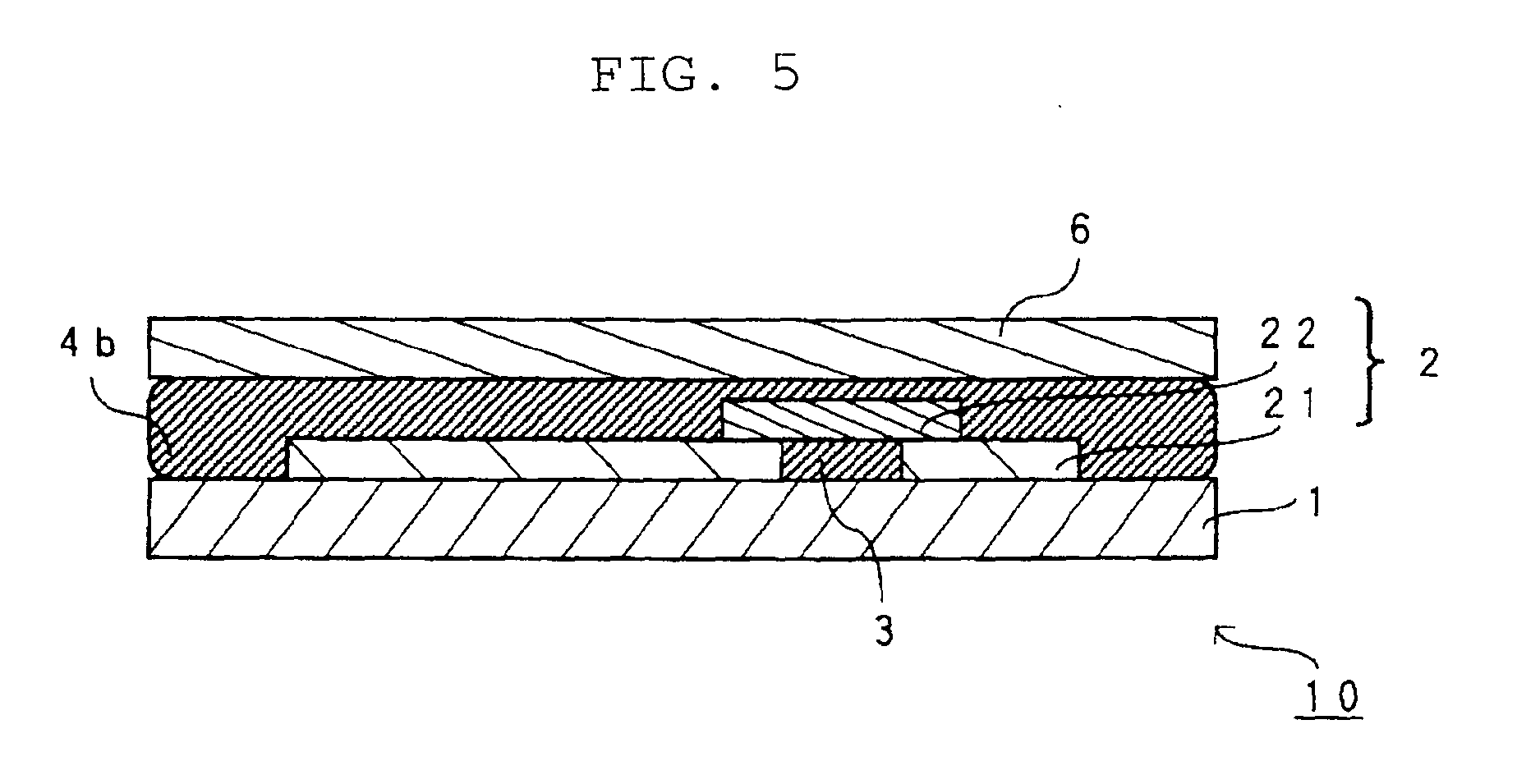
- Figure 5 is a sectional view schematically illustrating a stage where, after the transparent film is peeled, a cover film is laminated to the cured resin layer.
- step (1) in the process of the present invention may comprise, for example, the steps of:
- Figure 1 is a sectional view schematically illustrating a stage where a non-contact data carrier element 2 is formed on one surface la of a substrate film 1.
- the non-contact data carrier element 2 as shown in Fig. 1 contains an antenna circuit 21 and an IC chip 22 connected thereto.
- an irregular or uneven structure is formed which includes a protruded portion due to the antenna circuit 21, a protruded portion due to the IC chip 22 mounted on the antenna circuit 21, and depressed portions formed between the antenna circuit 21 and the IC chip 22.
- the non-contact data carrier element may be composed of the antenna circuit and the IC chip, but may further contain other electronic components, such as a battery, a capacitor, a resistor, a coil, a diode, a connective circult or the like.
- the non-contact data carrier element may be formed on one surface of the substrate film by any method known per se.
- a circuit such as the antenna circuit, may be formed by printing, etching, or sputtering on one surface of the substrate film 1.
- an IC chip, a battery, or a capacitor may be fixed or connected to the antenna circuit or to each other, with a solder or an electrically conductive resin to form the non-contact data carrier element.
- Figure 2 is a sectional view schematically illustrating a stage where a photo-curable resin composition 4a is applied as a droplet to the substrate film 1, on the surface la carrying the non-contact data carrier element 2. Then, the transparent film 5 is laminated on the photo-curable resin composition 4a, and the transparent film 5 is lightly pushed in the direction of the surface la of the substrate film 1 to spread the photo-curable resin composition 4a on the surface la and cover the whole non-contact data carrier element 2, as shown in Fig. 3.
- the photo-curable resin composition 4a has a viscosity sufficient to enable it to pour into and fill in the insides of the depressed portions. Therefore, as shown in Fig. 3, the photo-curable resin composition 4a enters deep to insides of the depressed portions 3 on the surface la, and these insides are completely filled with the photo-curable resin composition 4a. As a result, an entire surface of the non-contact data carrier element 2, including the protruded portions and the depressed portions thereof, are in close contact with the photo-curable resin composition 4a and thus protected thereby. It is sufficient that the photo-curable resin composition 4a completely covers the whole of the non-contact data carrier element 2, but preferably the photo-curable resin composition 4a covers the whole of the surface la.
- the process for forming the laminate is not limited, so long as the laminate as shown in Fig. 3 is produced.
- the photo-curable resin composition may be applied to the surface carrying the non-contact data carrier element on the substrate film, then pressed and spread to thereby cover the whole non-contact data carrier element, and thereafter the transparent film laminated thereon.
- one side of the transparent film may be coated with the photo-curable resin composition in the first place, and then laminated with the substrate film so that the surface carrying the photo-curable resin composition is brought into contact with the surface carrying the non-contact data carrier element, whereby the non-contact data carrier element may be completely covered with the photo-curable resin composition.
- the photo-curable resin composition in the laminate is cured. More particularly, as shown in Fig. 3, a light irradiation capable of curing the photo-curable resin composition is irradiated downward to the transparent film 5 of the laminate in the direction of the arrow A in Fig. 3. The light irradiation is passed through the transparent film 5 and reaches the photo-curable resin composition, to cure the photo-curable resin composition, whereby the photo-curable resin composition layer 4a is changed to the cured resin layer 4b (see Fig. 3).
- the laminate composed of the substrate film 1, the cured resin layer 4b containing the non-contact data carrier element 2, and the transparent film 5 is obtained.
- the photo-curable resin composition used in the present invention maintains a sufficient adhesiveness for the substrate film 1 after curing. Therefore, the cured resin layer 4b is in close contact with the substrate film 1, and the non-contact data carrier element 2 sandwiched therebetween is fully protected.
- a film which may be peeled from the cured resin layer 4b is used as the transparent film 5.
- the transparent film 5 may be peeled therefrom, and then, as shown in Fig. 5, the cover film 6 may be laminated to the cured resin layer 4b to obtain the resin-sealed non-contact data carrier 10.
- the cover film 6 may be printed to carry ornamental designs, before laminating. The printing procedure is easier in comparison with a printing after laminated.
- the photo-curable resin composition used in the process of the present invention exhibits a low viscosity before being optically cured, but is changed to the cured resin having a high adhesiveness after having been optically cured.
- the photo-curable resin composition having the above properties is composed of, for example, a curable component and a photopolymerization initiator.
- a curable component there may be mentioned, for example, an unsaturated polyester, a polyisoprene, a polybutadiene, a polyvinyl siloxane, an alkyl acrylate, an alkyl methacrylate, an acrylate modified phenol ethyleneoxide, an isobornyl acrylate, an acrylate modified bisphenolethyleneoxide, an acrylate modified ethyleneoxide isocyanarate, a tripropylene glycol diacrylate, a polyethylene glycol diacrylate, a pentaerythritol triacrylate, trimethylolpropane triacrylate, urethane acrylate, a polyester acylate, styrene, vinyl acetate, or vinyl pyrrolidone.
- the above curable component may be used singly, but in general several components may be combined to
- a ketone such as acetophenone, benzophenone, or Michler's ketone.
- the photopolymerization initiator is preferably used in an amount of 0.5 to 10 parts by weight with respect to 100 parts by weight of the curable component.
- the photo-curable resin composition may optionally contain, in addition to the above ingredients, a resin compound, such as a poly (meth)acrylate, a saturated polyester, a polyether, a urethane resin, or a silicone resin, a filler, such as titanium oxide or silica, a tackifier, such as a rosin ester or a terpene resin, an antioxidant, or a light stabilizer, or the like.
- a resin compound such as a poly (meth)acrylate, a saturated polyester, a polyether, a urethane resin, or a silicone resin
- a filler such as titanium oxide or silica
- a tackifier such as a rosin ester or a terpene resin
- an antioxidant or a light stabilizer, or the like.
- the photo-curable resin composition may be prepared by mixing the above ingredients in any sequential order.
- the photo-curable resin composition used in the process of the present invention preferably has a viscosity such that the photo-curable resin composition can pour into and fill in the insides of depressed portions of the irregular or uneven structure formed by mounting the non-contact data carrier element on the surface of the substrate film.
- the viscosity as above is preferably 5000 mPa ⁇ s or less, more preferably 10 mPa ⁇ s to 5000 mPa ⁇ s.
- the photo-curable resin composition with the viscosity of 5000 mPa ⁇ s or less can thoroughly pour into and completely fill in the insides of the depressed portions. When the viscosity is 10 mPa ⁇ s or more, the shape retention and process condition are improved.
- the substrate film and the transparent film may be coated with the photo-curable resin composition by any conventional method.
- care must be taken not to break the non-contact data carrier element.
- a die coater, a knife coater or the like may be used.
- the photo-curable resin composition may be cured by irradiation of, for example, a visible light, or preferably an ultraviolet light.
- the resulting cured resin must have adhere to the substrate film.
- the adhesiveness of the cured resin is preferably 0.5 N/25 mm or more, more preferably 0.5 N/25 mm to 100 N/25 m.
- the term "adhesiveness" as used herein means a value measured in accordance with a 180 degree peeling test in JIS (Japanese Industrial Standard) Z 0237, 8.3.1. If the adhesiveness is 0.5 N/25 mm or more, the cured resin is strongly bonded to the substrate film.
- the thickness of the cured resin layer is not particularly limited, but is preferably about 50 ⁇ m to 2 mm.
- the substrate film which may be used in the process of the present invention is not particularly limited, so long as it serves as a support capable of stably holding the non-contact data carrier element not only during each step production, but also in the resin-sealed non-contact data carrier produced according to the process of the present invention.
- the substrate film may be transparent or opaque.
- the substrate film may be, for example, a paper, a sheet of a natural or synthetic fibrous material, such as a woven fabric sheet, a knitted fabric sheet or a nonwoven fabric sheet, a synthetic resin film or sheet.
- the synthetic resin there may be mentioned, for example, a polyethylene, a polypropylene, a polyvinyl chloride, a polystyrene, a polyester such as a polyethylene terephthalate or a polyethylene naphthalate, a polyvinyl acetate, a polybutene, a polyacrylic acid, a polymethacrylic acid, a polyacrylate, a polymethacrylate, a polyvinyl alcohol, a polyvinyl formal, a polyvinyl butyral, a polyacrylonitrile, a polyimide, a polycarbonate, a polyamide, an ethylene-vinyl acetate copolymer, an ethylene acrylate copolymer, a polyviny
- the substrate film is preferably opaque.
- the opaque substrate film may be prepared by a method wherein an opacifying agent, such as titanium oxide or calcium carbonate is incorporated to the film, a method wherein the film surface is coated or printed with the opacifying agent together with a binder, a method wherein a blowing agent is used, or a method wherein talc having a poor compatibility with the film or the like is incorporated to the film, and the film then drawn to form micropores in the film, or the like.
- an opacifying agent such as titanium oxide or calcium carbonate
- the thickness of the substrate film is not particularly limited, but is preferably 50 ⁇ m to 2 mm.
- the transparent film which may be used in the process of the present invention is not particularly limited, so long as it can transmit the light capable of curing the photo-curable resin composition.
- the transparent film there may be mentioned, for example, a polyethylene film, a polypropylene film, a polyester film, or the like, or a film having a releasability imparted by coating the above film or a polyamide or polyvinyl chloride film with a silicone resin or a polymer of a long-chain aliphatic ester of (meth)acrylic acid.
- the thickness of the transparent film is not particularly limited, but is preferably 100 ⁇ m or less.
- the cover film which may be used in the process of the present invention is not particularly limited, so long as it exhibits a sufficient adhesiveness to the cured resin.
- the cover film there may be mentioned, for example, a paper, or a film of a polyester such as a polyethylene terephthalate or a polyethylene naphthalate, or a polyvinyl chloride, a polyethylene, a polypropylene, or an ethylene vinyl acetate.
- the sheet or film may be used singly, or as a laminate composed thereof.
- an internal structure of the non-contact data carrier should be concealed, from a standpoint of design or security.
- the cover film is preferably opaque.
- the opaque cover film may be prepared by the same method as those used when preparing the opaque substrate film as above.
- the cover film may be bonded to the cured resin by a method wherein the cover film is laminated after completing the curing step, a method wherein the cover film is laminated before completing the curing step, a method wherein the cover film is thermally bonded directly to the cured resin, or a method wherein a pressure-sensitive adhesive or a heat-sensitive adhesive is used.
- the thickness of the cover film is not particularly limited, but is preferably about 25 ⁇ m to 2 mm.
- An ornamental design may be printed on the surface of the substrate film and/or the cover film by a conventional printer or the like.
- a thin resin-sealed non-contact data carrier can be produced.
- an antenna circuit having a thickness of about 35 ⁇ m is mounted on one surface of a substrate film (50 mm X 80 mm) having a thickness of about 75 ⁇ m.
- an IC chip having a thickness of about 50 ⁇ m is placed on the antenna circuit.
- a cured resin layer having a thickness (i.e., an interval between the substrate film and the cover film) of about 100 ⁇ m is formed and a cover film having a thickness of about 75 ⁇ m is laminated thereto, to obtain a resin-sealed non-contact data carrier having a total thickness of about 250 ⁇ m.
- the surface of the cover film of the resulting resin-sealed non-contact data carrier is completely flat, and no affect due to an irregular or uneven internal structure is observed.
- the substrate film and the cover film are firmly laminated to each other, and do not separate from each other when the non-contact data carrier is used.
- Photo-curable resin compositions (A) to (D) composed of the following ingredients were prepared, and the viscosity (before curing) of each of the resulting photo-curable resin compositions (A) to (D) were measured, using a B-type viscometer at 25'C.
- the composition, viscosity, and adhesiveness (after curing) of each of the photo-curable resin compositions (A) to (D) are shown as follows.
- the surface carrying the non-contact data carrier element on the substrate was coated with the photo-curable resin composition (A).
- Ultraviolet light was applied thereto at 80W/cm 2 from a mercury vapor lamp, to cure the photo-curable resin composition.
- Example 1 The procedure disclosed in Example 1 was repeated, except that the photo-curable resin composition (B) was used instead of the photo-curable resin composition (A), to obtain a resin-sealed non-contact data carrier.
- Example 1 The procedure disclosed in Example 1 was repeated, except that the photo-curable resin composition (C) was used instead of the photo-curable resin composition (A), to obtain a resin-sealed non-contact data carrier.
- Example 1 The procedure disclosed in Example 1 was repeated, except that the photo-curable resin composition (D) was used instead of the photo-curable resin composition (A), to obtain a resin-sealed non-contact data carrier.
- a thermoplastic resin ethylene-vinyl acetate copolymer
- phenol resin phenol resin
- the non-contact data carrier element can be completely covered without damage, with the resin composition having a low viscosity and a good pourability before curing, and the resin can be optically cured to thereby prevent the non-contact data carrier element from damage during the curing step.
- the thin resin-sealed non-contact data carrier can be obtained while maintaining a smooth surface.
- the opaque cover film is used, the thin resin-sealed non-contact data carrier having an excellent opacifying property can be obtained with a simple procedure.
- the photo-curable resin composition is used, and thus the curing temperature is low. Therefore, a thin resin-sealed non-contact data carrier containing a built-in battery can be obtained without a liquid leakage from or a bursting of the battery.
Landscapes
- Engineering & Computer Science (AREA)
- Physics & Mathematics (AREA)
- General Physics & Mathematics (AREA)
- Theoretical Computer Science (AREA)
- Computer Hardware Design (AREA)
- Microelectronics & Electronic Packaging (AREA)
- Laminated Bodies (AREA)
Abstract
Description
| Adhesiveness to PET plate (N/25 mm) | Surface state | Dispatching /receiving test | Opacifying property of circuit | |
| Example 1 | 5 | | 5/5 | ○ |
| Example 2 | 4 | | 5/5 | ○ |
| Example 3 | 13 | | 5/5 | ○ |
| Example 4 | 15 | | 5/5 | ○ |
| Comparative Example 1 | 3 | 30 | 0/5 | × |
| Comparative Example 2 | 20 | 12 | 0/5 | ○ |
Claims (5)
- A process for producing a non-contact data carrier comprising the steps of:(1) forming a laminate containing a substrate film [1], a non-contact data carrier element [2] mounted on one surface [la] of said substrate film [1], a photo-curable resin composition layer [4b] formed to cover a whole of said non-contact data carrier element [2], and a transparent film [5] covering said photo-curable resin composition layer [4b], said transparent film [5] being peelable from a cured resin layer [4b] formed by curing said photo-curable resin composition;(2) irradiating said photo-curable resin composition with a light capable of curing said photo-curable resin composition through said transparent film [5] on said photo-curable resin composition layer [4a] to thereby cure said photo-curable resin composition, and form said cured resin layer [4b] embedding the whole of said non-contact data carrier element [2];(3) peeling said transparent film [5] from said cured resin layer [4b]; and(4) laminating a cover film [6] to said the cured resin layer [4b].
- The process according to claim 1, wherein said step (1) comprises(1a-1) coating the surface [la] of the substrate film [1] with the photo-curable resin composition to cover the whole non-contact data carrier element [2] therewith, whereby the photo-curable resin composition layer [4a] is formed; and then(1a-2) laminating the transparent film [5] on the photo-curable resin composition layer [4a].
- The process according to claim 1, wherein said step (1) comprises(1b-1) coating the transparent film [5] with the photo-curable resin composition; and then(1b-2) laminating the transparent film [5] on the surface [1a] of the substrate film [1] so that the whole non-contact data carrier element [2] is covered with the photo-curable resin composition on the transparent film [5].
- The process according to any one of claims 1 to 3, wherein a viscosity of said photo-curable resin composition is 5000 mPa·s or less.
- The process according to claim 4, wherein an adhesiveness of said cured resin formed by curing said photo-curable resin composition is 0.5 N/25 mm or more.
Applications Claiming Priority (2)
| Application Number | Priority Date | Filing Date | Title |
|---|---|---|---|
| JP769899 | 1999-01-14 | ||
| JP769899 | 1999-01-14 |
Publications (2)
| Publication Number | Publication Date |
|---|---|
| EP1020814A2 true EP1020814A2 (en) | 2000-07-19 |
| EP1020814A3 EP1020814A3 (en) | 2002-10-30 |
Family
ID=11673000
Family Applications (1)
| Application Number | Title | Priority Date | Filing Date |
|---|---|---|---|
| EP00100051A Withdrawn EP1020814A3 (en) | 1999-01-14 | 2000-01-05 | Process for producing non-contact data carrier |
Country Status (5)
| Country | Link |
|---|---|
| EP (1) | EP1020814A3 (en) |
| KR (1) | KR20000057738A (en) |
| CN (1) | CN1171173C (en) |
| SG (1) | SG91249A1 (en) |
| TW (1) | TW468137B (en) |
Cited By (5)
| Publication number | Priority date | Publication date | Assignee | Title |
|---|---|---|---|---|
| WO2004000965A1 (en) * | 2002-06-24 | 2003-12-31 | Loctite (R & D) Limited | Photocurable adhesive compositions, reaction products of which have low halide ion content |
| EP1120824A3 (en) * | 2000-01-27 | 2004-02-11 | LINTEC Corporation | Process for producing an ic chip having a protective layer |
| EP1211634A3 (en) * | 2000-12-04 | 2004-09-01 | Yupo Corporation | Tag and label comprising the same |
| WO2011054355A3 (en) * | 2009-11-06 | 2011-10-20 | Hegedues Viktor | Method for applying marking elements on an object; object comprising a marking element and use of a special material for applying a marking element on an object |
| WO2015086775A1 (en) * | 2013-12-11 | 2015-06-18 | Caretag Surgical Aps | Attachment and cover for an electronic identification tag |
Families Citing this family (3)
| Publication number | Priority date | Publication date | Assignee | Title |
|---|---|---|---|---|
| JP4143340B2 (en) * | 2002-06-17 | 2008-09-03 | 日立マクセル株式会社 | Non-contact communication type information carrier |
| DE102015012616A1 (en) * | 2014-10-16 | 2016-04-21 | Giesecke & Devrient Gmbh | Card body for a data carrier and inlay for a partial card body |
| CN104504430B (en) * | 2014-12-15 | 2021-06-29 | 苏州海博智能系统有限公司 | Electronic card manufacturing method |
Family Cites Families (10)
| Publication number | Priority date | Publication date | Assignee | Title |
|---|---|---|---|---|
| JPS60189586A (en) * | 1984-03-09 | 1985-09-27 | Dainippon Printing Co Ltd | Ic card carrier |
| JPS6314455A (en) * | 1986-07-07 | 1988-01-21 | Hitachi Maxell Ltd | Semiconductor device |
| JPH01272491A (en) * | 1988-04-25 | 1989-10-31 | Seiko Instr Inc | Mounting structure of semiconductor |
| JPH06122297A (en) * | 1992-08-31 | 1994-05-06 | Sony Chem Corp | IC card and method of manufacturing the same |
| US5852289A (en) * | 1994-09-22 | 1998-12-22 | Rohm Co., Ltd. | Non-contact type IC card and method of producing the same |
| JPH08185499A (en) * | 1994-12-27 | 1996-07-16 | Mitsubishi Chem Corp | Non-contact type IC card manufacturing method |
| JPH09109584A (en) * | 1995-10-19 | 1997-04-28 | Dainippon Printing Co Ltd | Non-contact IC card and method of manufacturing the same |
| JPH09315059A (en) * | 1996-05-31 | 1997-12-09 | Toppan Printing Co Ltd | IC card and method of manufacturing IC card |
| JPH1031847A (en) * | 1996-07-15 | 1998-02-03 | Canon Inc | ID card and method of manufacturing the same |
| JPH10147088A (en) * | 1996-11-20 | 1998-06-02 | Dainippon Printing Co Ltd | Non-contact type IC card and manufacturing method thereof |
-
2000
- 2000-01-03 SG SG200000024A patent/SG91249A1/en unknown
- 2000-01-05 EP EP00100051A patent/EP1020814A3/en not_active Withdrawn
- 2000-01-11 KR KR1020000001101A patent/KR20000057738A/en not_active Ceased
- 2000-01-11 TW TW089100309A patent/TW468137B/en not_active IP Right Cessation
- 2000-01-14 CN CNB001010638A patent/CN1171173C/en not_active Expired - Fee Related
Cited By (6)
| Publication number | Priority date | Publication date | Assignee | Title |
|---|---|---|---|---|
| EP1120824A3 (en) * | 2000-01-27 | 2004-02-11 | LINTEC Corporation | Process for producing an ic chip having a protective layer |
| EP1211634A3 (en) * | 2000-12-04 | 2004-09-01 | Yupo Corporation | Tag and label comprising the same |
| WO2004000965A1 (en) * | 2002-06-24 | 2003-12-31 | Loctite (R & D) Limited | Photocurable adhesive compositions, reaction products of which have low halide ion content |
| WO2011054355A3 (en) * | 2009-11-06 | 2011-10-20 | Hegedues Viktor | Method for applying marking elements on an object; object comprising a marking element and use of a special material for applying a marking element on an object |
| WO2015086775A1 (en) * | 2013-12-11 | 2015-06-18 | Caretag Surgical Aps | Attachment and cover for an electronic identification tag |
| US10182880B2 (en) * | 2013-12-11 | 2019-01-22 | Caretag Surgical Aps | Attachment and cover for an electronic identification tag |
Also Published As
| Publication number | Publication date |
|---|---|
| SG91249A1 (en) | 2002-09-17 |
| KR20000057738A (en) | 2000-09-25 |
| EP1020814A3 (en) | 2002-10-30 |
| CN1171173C (en) | 2004-10-13 |
| TW468137B (en) | 2001-12-11 |
| CN1260551A (en) | 2000-07-19 |
Similar Documents
| Publication | Publication Date | Title |
|---|---|---|
| JP4046167B2 (en) | Non-contact data carrier label | |
| US6648232B1 (en) | High temperature tag having enclosed transceiver | |
| JP3883652B2 (en) | IC carrier with plate frame and manufacturing method thereof | |
| JP2003520666A (en) | Method of manufacturing smart label material web and smart label material web | |
| EP1505537B1 (en) | Ic tag | |
| EP1120824A2 (en) | Process for producing an ic chip having a protective layer | |
| US20050253228A1 (en) | Method for encapsulation of a chipcard and module obtained thus | |
| NO177343C (en) | Device for adhering to hot adhesive foil | |
| EP1154391A1 (en) | Adhesion label | |
| KR20000057738A (en) | Process for producing non-contact data carrier | |
| TWI338863B (en) | Integrated circuit tag | |
| WO2008047705A1 (en) | Ic tag label | |
| JP2000268153A (en) | Manufacture of non-contact data carrier | |
| JP4743367B2 (en) | Tack label with RFID tag, manufacturing method of tack label with RFID tag, and manufacturing apparatus of tack label with RFID tag | |
| US20250322771A1 (en) | Rfid label for medical device | |
| JP2001195556A (en) | Label, label producing method, card and card producing method | |
| JP2002251140A (en) | Contactless data carrier label | |
| JP2023046869A (en) | RFID container and RFID container manufacturing method | |
| JP2017033436A (en) | IC tag label, IC tag label sheet, and IC tag label sheet manufacturing method | |
| JP2000073020A (en) | Production of minute article having tacky agent layer | |
| JPS6313543B2 (en) | ||
| GB2408037A (en) | Self-adhesive label incorporating magnetically-attachable label | |
| JP2005339429A (en) | Ic cartridge, and packing method and manufacturing method for ic card | |
| JP2002157567A (en) | Method for producing contact-type IC card and photocurable double-sided pressure-sensitive adhesive tape used for the same | |
| JP2006260227A (en) | IC card sheet manufacturing method, IC card |
Legal Events
| Date | Code | Title | Description |
|---|---|---|---|
| PUAI | Public reference made under article 153(3) epc to a published international application that has entered the european phase |
Free format text: ORIGINAL CODE: 0009012 |
|
| AK | Designated contracting states |
Kind code of ref document: A2 Designated state(s): AT BE CH CY DE DK ES FI FR GB GR IE IT LI LU MC NL PT SE |
|
| AX | Request for extension of the european patent |
Free format text: AL;LT;LV;MK;RO;SI |
|
| PUAL | Search report despatched |
Free format text: ORIGINAL CODE: 0009013 |
|
| AK | Designated contracting states |
Kind code of ref document: A3 Designated state(s): AT BE CH CY DE DK ES FI FR GB GR IE IT LI LU MC NL PT SE |
|
| AX | Request for extension of the european patent |
Free format text: AL;LT;LV;MK;RO;SI |
|
| 17P | Request for examination filed |
Effective date: 20030308 |
|
| AKX | Designation fees paid |
Designated state(s): DE FR IT NL |
|
| STAA | Information on the status of an ep patent application or granted ep patent |
Free format text: STATUS: THE APPLICATION HAS BEEN WITHDRAWN |
|
| 18W | Application withdrawn |
Effective date: 20050430 |