EP1018769A2 - Halbleiterbauelement mit erhöhter Gatterisolierungslebensdauer - Google Patents
Halbleiterbauelement mit erhöhter Gatterisolierungslebensdauer Download PDFInfo
- Publication number
- EP1018769A2 EP1018769A2 EP99309329A EP99309329A EP1018769A2 EP 1018769 A2 EP1018769 A2 EP 1018769A2 EP 99309329 A EP99309329 A EP 99309329A EP 99309329 A EP99309329 A EP 99309329A EP 1018769 A2 EP1018769 A2 EP 1018769A2
- Authority
- EP
- European Patent Office
- Prior art keywords
- layer
- electrode
- dielectric
- high bandgap
- dielectric layer
- Prior art date
- Legal status (The legal status is an assumption and is not a legal conclusion. Google has not performed a legal analysis and makes no representation as to the accuracy of the status listed.)
- Withdrawn
Links
Images
Classifications
-
- H—ELECTRICITY
- H10—SEMICONDUCTOR DEVICES; ELECTRIC SOLID-STATE DEVICES NOT OTHERWISE PROVIDED FOR
- H10D—INORGANIC ELECTRIC SEMICONDUCTOR DEVICES
- H10D62/00—Semiconductor bodies, or regions thereof, of devices having potential barriers
- H10D62/10—Shapes, relative sizes or dispositions of the regions of the semiconductor bodies; Shapes of the semiconductor bodies
- H10D62/13—Semiconductor regions connected to electrodes carrying current to be rectified, amplified or switched, e.g. source or drain regions
- H10D62/149—Source or drain regions of field-effect devices
- H10D62/151—Source or drain regions of field-effect devices of IGFETs
-
- H—ELECTRICITY
- H10—SEMICONDUCTOR DEVICES; ELECTRIC SOLID-STATE DEVICES NOT OTHERWISE PROVIDED FOR
- H10D—INORGANIC ELECTRIC SEMICONDUCTOR DEVICES
- H10D30/00—Field-effect transistors [FET]
- H10D30/60—Insulated-gate field-effect transistors [IGFET]
- H10D30/68—Floating-gate IGFETs
- H10D30/6891—Floating-gate IGFETs characterised by the shapes, relative sizes or dispositions of the floating gate electrode
-
- H—ELECTRICITY
- H10—SEMICONDUCTOR DEVICES; ELECTRIC SOLID-STATE DEVICES NOT OTHERWISE PROVIDED FOR
- H10D—INORGANIC ELECTRIC SEMICONDUCTOR DEVICES
- H10D64/00—Electrodes of devices having potential barriers
- H10D64/01—Manufacture or treatment
- H10D64/013—Manufacture or treatment of electrodes having a conductor capacitively coupled to a semiconductor by an insulator
- H10D64/01302—Manufacture or treatment of electrodes having a conductor capacitively coupled to a semiconductor by an insulator the insulator being formed after the semiconductor body, the semiconductor being silicon
- H10D64/01304—Manufacture or treatment of electrodes having a conductor capacitively coupled to a semiconductor by an insulator the insulator being formed after the semiconductor body, the semiconductor being silicon characterised by the conductor
- H10D64/01314—Manufacture or treatment of electrodes having a conductor capacitively coupled to a semiconductor by an insulator the insulator being formed after the semiconductor body, the semiconductor being silicon characterised by the conductor the conductor comprising a layer of Ge, C or of compounds of Si, Ge or C contacting the insulator
-
- H—ELECTRICITY
- H10—SEMICONDUCTOR DEVICES; ELECTRIC SOLID-STATE DEVICES NOT OTHERWISE PROVIDED FOR
- H10D—INORGANIC ELECTRIC SEMICONDUCTOR DEVICES
- H10D64/00—Electrodes of devices having potential barriers
- H10D64/01—Manufacture or treatment
- H10D64/031—Manufacture or treatment of data-storage electrodes
- H10D64/035—Manufacture or treatment of data-storage electrodes comprising conductor-insulator-conductor-insulator-semiconductor structures
-
- H—ELECTRICITY
- H10—SEMICONDUCTOR DEVICES; ELECTRIC SOLID-STATE DEVICES NOT OTHERWISE PROVIDED FOR
- H10D—INORGANIC ELECTRIC SEMICONDUCTOR DEVICES
- H10D64/00—Electrodes of devices having potential barriers
- H10D64/60—Electrodes characterised by their materials
- H10D64/66—Electrodes having a conductor capacitively coupled to a semiconductor by an insulator, e.g. MIS electrodes
- H10D64/667—Electrodes having a conductor capacitively coupled to a semiconductor by an insulator, e.g. MIS electrodes the conductor comprising a layer of alloy material, compound material or organic material contacting the insulator, e.g. TiN workfunction layers
-
- H—ELECTRICITY
- H10—SEMICONDUCTOR DEVICES; ELECTRIC SOLID-STATE DEVICES NOT OTHERWISE PROVIDED FOR
- H10D—INORGANIC ELECTRIC SEMICONDUCTOR DEVICES
- H10D64/00—Electrodes of devices having potential barriers
- H10D64/60—Electrodes characterised by their materials
- H10D64/66—Electrodes having a conductor capacitively coupled to a semiconductor by an insulator, e.g. MIS electrodes
- H10D64/667—Electrodes having a conductor capacitively coupled to a semiconductor by an insulator, e.g. MIS electrodes the conductor comprising a layer of alloy material, compound material or organic material contacting the insulator, e.g. TiN workfunction layers
- H10D64/669—Electrodes having a conductor capacitively coupled to a semiconductor by an insulator, e.g. MIS electrodes the conductor comprising a layer of alloy material, compound material or organic material contacting the insulator, e.g. TiN workfunction layers the conductor further comprising additional layers of alloy material, compound material or organic material, e.g. TaN/TiAlN
-
- H—ELECTRICITY
- H10—SEMICONDUCTOR DEVICES; ELECTRIC SOLID-STATE DEVICES NOT OTHERWISE PROVIDED FOR
- H10D—INORGANIC ELECTRIC SEMICONDUCTOR DEVICES
- H10D62/00—Semiconductor bodies, or regions thereof, of devices having potential barriers
- H10D62/80—Semiconductor bodies, or regions thereof, of devices having potential barriers characterised by the materials
- H10D62/83—Semiconductor bodies, or regions thereof, of devices having potential barriers characterised by the materials being Group IV materials, e.g. B-doped Si or undoped Ge
- H10D62/832—Semiconductor bodies, or regions thereof, of devices having potential barriers characterised by the materials being Group IV materials, e.g. B-doped Si or undoped Ge being Group IV materials comprising two or more elements, e.g. SiGe
- H10D62/8325—Silicon carbide
Definitions
- the present invention is directed to a semiconductor device and a process for fabricating the device.
- a number of semiconductor devices have a structure in which two electrodes are separated by a layer of dielectric material.
- a MOSFET metal-oxide-semiconductor field effect transistor
- a MOSFET device is a voltage-controlled device that has a channel region linking two electrically-separated, highly conductive regions of a first conductivity type diffused into an opposite conductivity type semiconductor substrate.
- V TH threshold voltage
- the voltage that is applied to the device causes one electrode (the cathode) to inject electrons across the dielectric layer and into the other electrode (the anode).
- the cathode the cathode
- the anode the electrode that inject electrons across the dielectric layer and into the other electrode (the anode).
- the electrons are injected into the anode with high energies (i.e. energies that are above the conduction band edge of the anode material). Such high energies are typically above about 0.2 eV.
- the electron injection energy (E j ) is defined herein with respect to the conduction band edge of the anode material.
- High-energy electrons in the anode undergo impact ionization, which creates holes.
- Electron impact ionization is the process in which a high-energy electron collides with a valence electron. This collision promotes the valence electron into a higher energy empty state either in the valence band or the conduction band. The promotion of the valence electron leaves behind an energetic hole in the valence band.
- An energetic hole has an energy that is typically 0.2 eV greater than the valence band edge in the anode material.
- hole injection or anode injection refer to energetic hole injection from the anode into the dielectric material.
- the rate of impact ionization is a strong function of E j (decreasing as E j decreases) and of the band gap of the anode material (decreasing as the band gap increases).
- the present invention is directed to a semiconductor device in which a dielectric material is interposed between two electrodes.
- Examples of such devices include active devices such as metal oxide semiconductor field effect transistors (MOSFET), charge-coupled devices, and floating gate memory devices (e.g. EEPROM devices) and passive devices such as capacitors.
- MOSFET metal oxide semiconductor field effect transistors
- EEPROM devices floating gate memory devices
- passive devices such as capacitors.
- the device of the present invention is designed to reduce the amount of damage to the dielectric material of the device during device operation. By reducing the amount of damage to the dielectric material over time, the lifetime of the device is extended.
- the present invention is a semiconductor device wherein the number of holes that penetrate the dielectric (typically SiO 2 ) material is reduced (compared to prior art devices) over time. The rate at which the dielectric is damaged by hole penetration is commensurately reduced.
- the number of holes that penetrate the dielectric are controlled by selecting an electrode material that does one or more of the following: 1.) reduces the number of electrons incident from the cathode to the anode; 2.) reduces the probability that electrons incident on the anode will produce holes by undergoing impact ionization; and 3.) reduces the total energy of the holes produced by impact ionization (thereby decreasing the probability that the holes will be injected from the anode into the dielectric material).
- the high bandgap material is electrically conductive (i.e., it serves as a conducting electrode containing free carriers).
- the high bandgap material is doped.
- the dopant can be either n-type or p-type, depending upon the nature of the materials adjacent to the high bandgap material and other device considerations.
- the doping results in a high bandgap material having a single conductivity type (either dominated by electrons or holes).
- the majority dopant is either n-type (dominated by electrons) or p-type (dominated by holes). Consequently, the layer of high bandgap material functions as an electrode.
- the electrode with the high band gap material is either the high band gap material alone or a composite electrode that has more than one material layer. In the composite electrode embodiments, the high bandgap material must be the material that is adjacent to (i.e. next to and in contact with) the dielectric layer.
- the present invention is directed to any semiconductor device in which the dielectric material is between two electrodes.
- the invention is described in terms of a MOSFET device.
- the dielectric layer is the gate dielectric layer.
- applicants refer to a MOSFET devices and gate dielectric layers for example only, and the invention is not to be construed as limited to MOSFET devices or gate dielectric layers.
- the gate dielectric layer is SiO 2 .
- SiO 2 is susceptible to damage when penetrated by holes.
- SiO 2 is one of a class of electrically insulating materials that have a relatively large bandgap. Hole penetration into such materials induces the formation of charge traps which, in turn, may cause changes (either structural or electrical) in the material that adversely affect its dielectric properties. Consequently, the present invention is suited for use in any semiconductor device which has a dielectric material that is susceptible to damage when penetrated by holes.
- the MOSFET gate dielectric layer is formed on a silicon substrate and the electrode formed on top of the gate dielectric layer is typically polycrystalline silicon. The device of the present invention creates an environment that reduces the number of holes that will penetrate the gate dielectric layer by placing a layer of high bandgap material adjacent to the dielectric layer.
- the gate dielectric layer is formed on a semiconductor substrate with source and drain regions formed therein.
- the high bandgap material is formed over the gate dielectric layer (i.e. the dielectric layer is between the high bandgap layer and the substrate).
- the high bandgap material is electrically conductive.
- the remaining portion of the gate is then formed over the layer of high bandgap material.
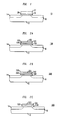
- FIG. 1 is a schematic cross-section of a device of the present invention in which a layer of high bandgap material is formed over the gate dielectric layer.
- FIG. 2A is a schematic cross-section of a second embodiment of a device of the present invention.
- FIG. 2B is a schematic cross-section of a third embodiment of a device of the present invention.
- FIG. 2C is a schematic cross-section of a fourth embodiment of a device of the present invention.
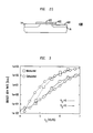
- FIG. 2D is a schematic cross-section of a fifth embodiment of a device of the present invention.
- FIG. 3 is a comparison of simulated and measured damage generation rates in an SiO 2 gate dielectric layer as a function of gate voltage.
- the present invention is directed to a semiconductor device that has a dielectric material layer sandwiched between two electrode materials.
- a layer of high bandgap material is provided adjacent to the dielectric layer that reduces the damage to the dielectric material during device operation compared to prior art devices. Damage during device operation is attributed at least in part to holes that are injected into the dielectric layer.
- the dielectric material in the device of the present invention is less susceptible to damage than prior art devices because the high bandgap material reduces the number of holes that are injected into the gate dielectric material compared to prior art devices.
- the hole flux (I h ) is the product of three factors.
- the first factor is the number of electrons incident from the cathode to the anode (I e ).
- the second is the probability that the electrons incident on the anode will undergo impact ionization (P ii ).
- I e depends on the energy barrier between the cathode and the dielectric. Increasing this barrier decreases the number of electrons injected.
- P ii is a strong function of the electron energy. For example, when a large density of holes is not present in the anode, a good approximation for the rate of impact ionization for an initial electron of energy E j yields, P ii (E j ) ⁇ ⁇ dE 3 ⁇ dE H ⁇ C (E 3 ) ⁇ V (E H ) ⁇ C (E j -E H -E g -E 3 ) where ⁇ c(E) and ⁇ v(E) are total conduction and valence band densities of states.
- E 3 is the energy of the final state of the initial electron
- E H is the energy of the hole produced in the collision with respect to the anode valence band edge
- E g is the band gap energy.
- P ii is the probability of a collision between a conduction electron and a valence electron;
- equation (1) represents the total combined density of states available for the products of that collision (final states) and the density of the initial target valence electrons present. This combined density of states is reduced strongly when E j - E g becomes close to zero since the densities of states ⁇ C (E) and ⁇ V (E) go as E 1 ⁇ 2 as E approaches zero, and are zero for E ⁇ 0.
- the probability of impact ionization is reduced as the bandgap of the anode increases, and as E j decreases. Consequently, all other things being equal, a decreased rate of impact ionization occurs in a device with a high bandgap material anode compared to the same device with a silicon anode.
- the presence of the high bandgap material reduces the number of holes that are created (compared to the same device operated in the same manner but with a silicon anode) that penetrate and, therefore damage the dielectric layer.
- T h is the probability that holes in the anode will penetrate the dielectric (where they can cause damage). T h decreases strongly (exponentially) with an increasing barrier for holes to enter the dielectric from the anode. T h is also a strongly increasing function of hole energy, and therefore the larger the maximum energy of holes created in the anode the higher the probability of penetrating the dielectric.
- the generation probability of a hole of energy E H due to impact ionization of the initial electron of energy E j follows from (1) above and is proportional to ⁇ V (E H ) ⁇ dE 3 ⁇ C (E 3 ) ⁇ C (E j -E H -E g -E 3 ).
- E MAX E j - E g .
- E j and E g directly impact E MAX . Reducing E j or increasing E g will directly reduce E MAX . Since T h is a strongly increasing function of E MAX , reducing E j or increasing E g will strongly suppress I h .
- the presence of the high bandgap material reduces the number of holes that penetrate the dielectric (compared to the same device operated in the same manner but with a silicon anode) and, therefore, damage the dielectric layer.
- the material properties of the anode and cathode affect the number of holes injected into the dielectric and hence the dielectric damage rate by affecting the number and energy distribution of holes created in the anode, as detailed above.
- the effect of the high bandgap material on these factors depends upon both device structure and device operation.
- the effect of the high bandgap material on these factors is explained by comparing the effect of the high bandgap material with the effect of silicon.
- the high bandgap material not only has a different bandgap than silicon, its conduction band edge and/or valence band edge are also typically different.
- the difference between the band gap of the high bandgap material and the bandgap of silicon is referred to as ⁇ E g .
- ⁇ E g E g X - E g silicon .
- the E g for a semiconductor material is positive.
- a positive ⁇ E g indicates that the high bandgap materials have a bandgap greater than that of silicon.
- the conduction band edge is the energy of the lowest energy electron state that is in the conduction band of the material.
- the difference between the energy of the conduction band edge of the high bandgap material and the conduction band edge of silicon is defined in terms of the electron affinity, ⁇ .
- the electron affinity, ⁇ , of a material is the difference in energy between the vacuum level and the conduction band edge of the material. This energy is positive when an electron has a lower energy at the conduction band edge than in vacuum.
- the difference between the conduction band edge of the high bandgap material and that of silicon is the conduction band offset and is designated as ⁇ E C .
- the valence band edge is the energy of the most energetic electron state that is in the valence band.
- the difference between the energy of the valence band edge of the high bandgap material and the valence band edge of silicon is referred to as the valence band offset and is designated as ⁇ E V .
- the high bandgap material provides the following benefits compared with silicon.
- the dielectric-anode interface does not contain holes (for example the n-gate in an n-gate/n-channel device) and the device has a high bandgap material anode adjacent the dielectric layer instead of a silicon anode adjacent thereto, the probability of hole creation (P ii ) is reduced.
- the probability is reduced because the bandgap of the anode is increased ( ⁇ Eg > 0) above the bandgap for silicon.
- E j the electron injection energy with respect to the conduction band bottom, E j , is lowered. This reduces the probability of hole creation (P ii ) and thereby reduces the final energy of the holes, which, additionally, reduces the hole transmission probability (T h ).
- the dielectric-anode interface contains holes (for example p-channel in n-gate/p-channel, or p-channel in p-gate/p-channel) and the device has a high bandgap material anode adjacent to the dielectric layer instead of a silicon anode adjacent thereto, and, if ⁇ E c > 0, the electron injection energy with respect to the conduction band bottom, E j , is lowered. This reduces the probability of hole creation (P ii ) and thereby reduces the final energy of the holes, which, in turn, reduces the hole transmission probability (T h ).
- holes for example p-channel in n-gate/p-channel, or p-channel in p-gate/p-channel
- the dielectric-cathode interface contains holes (for example p-gate in p-channel/p-gate device) and the device has a high bandgap material cathode adjacent to the dielectric layer instead of a silicon cathode adjacent thereto, then, when ⁇ E V > 0, the barrier to electrons tunneling from the valence band of the injection terminal layer is increased. Increasing this barrier lowers the total number of electrons incident on the anode (I e ). The electron injection energy with respect to conduction band bottom, E j , is also lowered, thereby reducing the probability of hole creation (P ii ) and the final energy of the holes, which, in turn, reduces the hole transmission probability (T h ).
- holes for example p-gate in p-channel/p-gate device
- the present invention contemplates devices in which the electrode is a composite of a high bandgap material adjacent to the dielectric layer and a low bandgap material (e.g. doped silicon).
- the device is advantageous over prior art devices in which the low bandgap material is adjacent to the dielectric.
- the advantage derives from the fact that, in the devices of the present invention, the holes that are produced in the low bandgap material cause less damage to the dielectric layer compared to the damage caused by holes produced in the low bandgap material in prior art devices.
- the damage efficiency of the holes is reduced because the holes lose energy due to scattering as they travel toward the dielectric material and through the high bandgap material, and thus their T h is reduced and, consequently, I h is lowered.
- the high bandgap material has a bandgap that is greater than 1.1 eV.
- suitable high bandgap materials include silicon carbide (SiC), diamond and gallium nitride (GaN).
- the bandgap for SiC (the 4H form) is 3.2 eV.
- the bandgap for diamond is 5.5 eV and the bandgap for GaN is 3.5 eV. Comparing SiC with silicon, the ⁇ E V is 0.2 eV and the AE c is 2.0 eV.
- the high bandgap material is an electrode
- the high bandgap material must be capable of being doped in order to obtain the desired conductivity.
- the high bandgap material is doped to achieve a single conductivity type (i.e. dominated by electrons or holes). The particular conductivity type will depend on the operating conditions of the device.
- the conductivity type is also restricted by the conductivity type in the other layer. Specifically, if the high bandgap material is adjacent to a doped, semiconductor electrode (e.g. doped, polycrystalline silicon) then the high bandgap material is the same conductivity type as the doped semiconductor. If the high bandgap material is adjacent to a metal electrode, then the conductivity type of the high bandgap material is not so restricted.
- dopant As a particular device, and such selection is readily made by one skilled in the art. Also, one skilled in the art is readily able to select the manner (e.g. in situ dopant or implant) in which the dopant is introduced into the high bandgap material. For example, doping SiC with both n- and p-type dopants is described in Itoh, A, et al., “Single Crystal Growth of SiC and Electronic Devices," Critical Reviews in Solid State and Materials Sciences , Vol. 22, No. 2 (1997), which is hereby incorporated by reference.
- FIG. 1 A schematic cross-section of one embodiment of the device of the present invention is illustrated in FIG. 1.
- That device 10 is a MOSFET.
- the device is formed on a silicon substrate 12 that has source 14 and drain 16 regions formed therein.
- a layer of dielectric material 18 is formed on the substrate.
- the layer of dielectric material is a material that is susceptible to damage by hole penetration during device operation.
- One example of such a material is SiO 2 .
- a layer of a high bandgap material 20 is formed over the gate dielectric layer and is doped to provide the requisite conductivity.
- the high bandgap material is doped either in situ as the material is being formed on the gate dielectric layer or by implantation.
- the remaining portion of the gate 22 is formed over the layer of high bandgap material 20.
- Suitable gate structures for MOSFET devices are well known to one skilled in the art and are not described in detail herein. Tungsten silicide is one example of a suitable material for the remaining portion of the gate.
- FIG. 2A A second embodiment of the present invention is illustrated in FIG. 2A.
- the device 100 depicted in FIG. 2A is a floating gate memory device.
- the device 100 has a first dielectric layer 101 and a second dielectric layer 102.
- Layers 103 and 104 together are a composite electrode.
- Layer 103 is a layer of conductive, high bandgap material.
- Layer 104 is a layer of conductive material such as doped polysilicon.
- the high bandgap material layer 103 is adjacent the second dielectric layer 102.
- layer 102 is the layer that is protected from damage due to hole penetration by the presence of the high bandgap material layer 103.
- a second gate 105 is formed over the second dielectric layer 102.
- FIG. 2B A third embodiment of the present invention is illustrated in FIG. 2B.
- the device 200 depicted in FIG. 2B is a floating gate memory device.
- the device has a first dielectric layer 180 and a second dielectric layer 240.
- Layer 201 is a layer of conductive, high bandgap material.
- Layer 260 is a layer of conductive material.
- the high bandgap material layer 201 is adjacent the second dielectric layer 240.
- layer 240 is the layer that is protected from damage due to hole penetration by the presence of the high bandgap material layer 200.
- the remaining portion of the gate 220 is formed over the high bandgap material layer 201.
- FIG. 2C A fourth embodiment of the present invention is illustrated in FIG. 2C.
- the device 300 depicted in FIG. 2C is a floating gate memory device.
- the device has a first dielectric layer 318 and a second dielectric layer 324.
- Layer 320 is a layer of conductive, high bandgap material.
- the high bandgap material layer 320 is adjacent to the first dielectric layer 318 and to the second dielectric layer 324.
- a gate 322 is formed over the second dielectric layer 24.
- FIGS. 2A-2C show the stacked dielectric/electrode/dielectric/electrode structure spanning the entire channel.
- the present invention is not limited to devices with this structure.
- the present invention also contemplates split-gate devices in which the stacked dielectric/electrode/dielectric/electrode structure is formed over only a portion of the channel.
- the device 400 is a transistor in which the high bandgap electrode 401 is in the drain electrode 16.
- the high bandgap material is doped to achieve a single conductivity type, and that conductivity type is the same as the conductivity type for the drain electrode 16.
- the high bandgap electrode 401 is adjacent the gate dielectric layer 402.
- the gate 403 of the device 400 is formed over the gate dielectric layer. In this embodiment, only the portion of the gate dielectric layer 402 in contact with the high bandgap material is protected from damage due to hole penetration.
- FIG. 1 An example of a processing sequence for fabricating the MOSFET device described in FIG. 1 is described below.
- One skilled in the art will appreciate that a variety of different processing sequences are useful for forming the devices of the present invention.
- the following sequence is provided for illustrative purposes, and is not intended to limit the scope of the invention in any way.
- the device illustrated in FIG. 1 is formed by defining device regions in the substrate, i.e. doping the substrate to form source, drain and channel regions, and for forming insulating regions for device isolation. Such steps are well known to one skilled in the art and are not described in detail herein.
- the device dielectric layer is formed on the substrate surface.
- the material for the device dielectric layer is any material that has suitable dielectric properties and is compatible with the overall process for device fabrication. Silicon dioxide (SiO 2 ) is by far the most common dielectric material used for the gate dielectric in processes for fabricating MOSFETs. As previously noted, other materials that are susceptible to hole damage are also contemplated as suitable.
- the layer of dielectric material is formed on the substrate using conventional expedients well known to one skilled in the art.
- the dielectric material is SiO 2
- the dielectric is formed by subjecting the substrate to an elevated temperature in the range of about 850°C to about 1050°C in an oxygen-containing atmosphere. Suitable conditions for forming SiO 2 of a desired thickness are well known to one skilled in the art.
- a layer of high bandgap material is formed over the substrate.
- the deposition conditions will depend upon the material selected. For example if the material is a SiC film, the material may be deposited using the conditions described in Bassler, M., et al., "Interface State Density as Implanted 6H-SiC/SiO 2 MOS Structures," Mater. Sci. Forum , Vol. 264-268, Pt. 2, pp. 861-864 (1998).
- the high bandgap material is doped so that the material is sufficiently conductive.
- the thickness of the high bandgap material is at least several times the mean inelastic scattering distance for high energy electrons.
- the inelastic scattering distance is the distance than an electron travels before it loses energy.
- the layer of high bandgap material is required to be at least several monolayers thick. The high bandgap material thickness is further selected so that it does not adversely affect device performance.
- the remaining portion of the gate stack is formed.
- the subsequent process sequence depends upon the desired gate stack. For example, in some embodiments subsequent layers of metal silicide or polysilicon are formed over the layer of high bandgap material.
- the processes and materials for forming the subsequent gate stack materials are conventional and are not described in detail herein.
- FIG. 3 illustrates the relationship between the rate of damage generation and the gate voltage applied to a capacitor.
- This capacitor had a 3.5nm thick SiO 2 dielectric, an n-doped poly-silicon gate and a p-doped Si substrate.
- the measurements were provided in DiMaria, D, et al , Appl. Phys. Lett. , Vol. 68, p.3004 (1996).
- the simulations were performed with a physically-based simulator which computes hole current injection from the anode into the dielectric (I h ) as a function of voltage applied to the gate.
- I h hole current injection from the anode into the dielectric
- These anode hole currents are computed following a similar model as described in equations (1) through (3) and share the same dependencies on E g and E j as described herein.
- This plot shows that dielectric damage is proportional to the anode hole current, and that the models presented in equations (1) through (3) provide an accurate assessment of this damage
Landscapes
- Insulated Gate Type Field-Effect Transistor (AREA)
- Electrodes Of Semiconductors (AREA)
- Solid State Image Pick-Up Elements (AREA)
- Semiconductor Memories (AREA)
- Non-Volatile Memory (AREA)
Applications Claiming Priority (4)
| Application Number | Priority Date | Filing Date | Title |
|---|---|---|---|
| US271084 | 1981-06-05 | ||
| US11071198P | 1998-12-03 | 1998-12-03 | |
| US110711P | 1998-12-03 | ||
| US09/271,084 US6531751B1 (en) | 1998-12-03 | 1999-03-17 | Semiconductor device with increased gate insulator lifetime |
Publications (2)
| Publication Number | Publication Date |
|---|---|
| EP1018769A2 true EP1018769A2 (de) | 2000-07-12 |
| EP1018769A3 EP1018769A3 (de) | 2000-12-27 |
Family
ID=26808328
Family Applications (1)
| Application Number | Title | Priority Date | Filing Date |
|---|---|---|---|
| EP99309329A Withdrawn EP1018769A3 (de) | 1998-12-03 | 1999-11-23 | Halbleiterbauelement mit erhöhter Gatterisolierungslebensdauer |
Country Status (3)
| Country | Link |
|---|---|
| US (1) | US6531751B1 (de) |
| EP (1) | EP1018769A3 (de) |
| JP (1) | JP2000174276A (de) |
Cited By (1)
| Publication number | Priority date | Publication date | Assignee | Title |
|---|---|---|---|---|
| TWI787089B (zh) * | 2022-02-18 | 2022-12-11 | 旺宏電子股份有限公司 | 半導體元件 |
Families Citing this family (3)
| Publication number | Priority date | Publication date | Assignee | Title |
|---|---|---|---|---|
| US6830953B1 (en) * | 2002-09-17 | 2004-12-14 | Taiwan Semiconductor Manufacturing Company, Ltd. | Suppression of MOSFET gate leakage current |
| US20050269621A1 (en) * | 2004-06-03 | 2005-12-08 | Micron Technology, Inc. | Flash memory devices on silicon carbide |
| US7195983B2 (en) * | 2004-08-31 | 2007-03-27 | Freescale Semiconductor, Inc. | Programming, erasing, and reading structure for an NVM cell |
Family Cites Families (12)
| Publication number | Priority date | Publication date | Assignee | Title |
|---|---|---|---|---|
| US3673471A (en) | 1970-10-08 | 1972-06-27 | Fairchild Camera Instr Co | Doped semiconductor electrodes for mos type devices |
| JPS5656677A (en) | 1979-10-13 | 1981-05-18 | Toshiba Corp | Semiconductor memory device |
| JPS6358871A (ja) * | 1986-08-28 | 1988-03-14 | Fujitsu Ltd | 半導体装置 |
| JPS63150963A (ja) * | 1986-12-12 | 1988-06-23 | Fujitsu Ltd | 半導体装置 |
| US4980303A (en) * | 1987-08-19 | 1990-12-25 | Fujitsu Limited | Manufacturing method of a Bi-MIS semiconductor device |
| JP2546696B2 (ja) * | 1987-12-17 | 1996-10-23 | 富士通株式会社 | シリコン炭化層構造 |
| JPH03222367A (ja) | 1990-01-26 | 1991-10-01 | Fujitsu Ltd | 絶縁ゲート型電界効果トランジスタ |
| US5307305A (en) | 1991-12-04 | 1994-04-26 | Rohm Co., Ltd. | Semiconductor device having field effect transistor using ferroelectric film as gate insulation film |
| JP3305197B2 (ja) * | 1995-09-14 | 2002-07-22 | 株式会社東芝 | 半導体装置 |
| US5801401A (en) | 1997-01-29 | 1998-09-01 | Micron Technology, Inc. | Flash memory with microcrystalline silicon carbide film floating gate |
| US5886368A (en) * | 1997-07-29 | 1999-03-23 | Micron Technology, Inc. | Transistor with silicon oxycarbide gate and methods of fabrication and use |
| US6031263A (en) * | 1997-07-29 | 2000-02-29 | Micron Technology, Inc. | DEAPROM and transistor with gallium nitride or gallium aluminum nitride gate |
-
1999
- 1999-03-17 US US09/271,084 patent/US6531751B1/en not_active Expired - Lifetime
- 1999-11-23 EP EP99309329A patent/EP1018769A3/de not_active Withdrawn
- 1999-12-03 JP JP11344557A patent/JP2000174276A/ja active Pending
Non-Patent Citations (1)
| Title |
|---|
| Physics of Semiconductor Devices, S.M. Sze, John Wiley & Sons, 1981, p. 850 * |
Cited By (1)
| Publication number | Priority date | Publication date | Assignee | Title |
|---|---|---|---|---|
| TWI787089B (zh) * | 2022-02-18 | 2022-12-11 | 旺宏電子股份有限公司 | 半導體元件 |
Also Published As
| Publication number | Publication date |
|---|---|
| EP1018769A3 (de) | 2000-12-27 |
| US6531751B1 (en) | 2003-03-11 |
| JP2000174276A (ja) | 2000-06-23 |
Similar Documents
| Publication | Publication Date | Title |
|---|---|---|
| US9490338B2 (en) | Silicon carbide semiconductor apparatus and method of manufacturing same | |
| US5349225A (en) | Field effect transistor with a lightly doped drain | |
| US6084268A (en) | Power MOSFET device having low on-resistance and method | |
| US7485895B2 (en) | Silicon carbide semiconductor device | |
| US7696540B2 (en) | Structure and method for a fast recovery rectifier structure | |
| CN109728097B (zh) | 一种功率半导体mos器件及其制备方法 | |
| TW405225B (en) | Semiconductor device and manufacturing method therefor | |
| US10050137B2 (en) | Enhanced normally-off high electron mobility heterojunction transistor | |
| EP0809865A1 (de) | Halbleiterfeldeffektanordnung mit einer sige schicht | |
| JPH0818045A (ja) | 時間依存性絶縁破損を減少させた半導体デバイス | |
| US20060202254A1 (en) | Multi-level flash memory cell capable of fast programming | |
| JP2021114496A (ja) | 縦型窒化物半導体トランジスタ装置 | |
| US7074681B2 (en) | Semiconductor component and method of manufacturing | |
| US11581401B2 (en) | Pin diode including a conductive layer, and fabrication process | |
| JP2009135494A (ja) | 消去飽和について改善したイミュニティを備えた不揮発性メモリデバイスおよびその製造方法 | |
| US6639272B2 (en) | Charge compensation semiconductor configuration | |
| KR100762545B1 (ko) | Lmosfet 및 그 제조 방법 | |
| TWI829085B (zh) | 的碳化矽金屬氧化物半導體場效電晶體 | |
| US4783688A (en) | Schottky barrier field effect transistors | |
| US20240088229A1 (en) | Low gate current junction field effect transistor device architecture | |
| US4486766A (en) | Schottky barrier field effect transistors | |
| KR101286704B1 (ko) | 매몰절연막에 고정 전하층을 갖는 트랜지스터 및 그 제조방법 | |
| US6531751B1 (en) | Semiconductor device with increased gate insulator lifetime | |
| JP3221901B2 (ja) | 半導体装置 | |
| US20240266401A1 (en) | Transistor device and manufacturing method thereof |
Legal Events
| Date | Code | Title | Description |
|---|---|---|---|
| PUAI | Public reference made under article 153(3) epc to a published international application that has entered the european phase |
Free format text: ORIGINAL CODE: 0009012 |
|
| 17P | Request for examination filed |
Effective date: 19991201 |
|
| AK | Designated contracting states |
Kind code of ref document: A2 Designated state(s): DE FR GB |
|
| AX | Request for extension of the european patent |
Free format text: AL;LT;LV;MK;RO;SI |
|
| PUAL | Search report despatched |
Free format text: ORIGINAL CODE: 0009013 |
|
| RIC1 | Information provided on ipc code assigned before grant |
Free format text: 7H 01L 29/51 A, 7H 01L 21/28 B, 7H 01L 29/49 B, 7H 01L 29/08 B |
|
| AK | Designated contracting states |
Kind code of ref document: A3 Designated state(s): AT BE CH CY DE DK ES FI FR GB GR IE IT LI LU MC NL PT SE |
|
| AX | Request for extension of the european patent |
Free format text: AL;LT;LV;MK;RO;SI |
|
| 17Q | First examination report despatched |
Effective date: 20010215 |
|
| AKX | Designation fees paid |
Free format text: DE FR GB |
|
| STAA | Information on the status of an ep patent application or granted ep patent |
Free format text: STATUS: THE APPLICATION IS DEEMED TO BE WITHDRAWN |
|
| 18D | Application deemed to be withdrawn |
Effective date: 20010828 |