EP1012500B1 - Sources et systemes d'eclairage - Google Patents
Sources et systemes d'eclairage Download PDFInfo
- Publication number
- EP1012500B1 EP1012500B1 EP97932394A EP97932394A EP1012500B1 EP 1012500 B1 EP1012500 B1 EP 1012500B1 EP 97932394 A EP97932394 A EP 97932394A EP 97932394 A EP97932394 A EP 97932394A EP 1012500 B1 EP1012500 B1 EP 1012500B1
- Authority
- EP
- European Patent Office
- Prior art keywords
- output
- waveguide
- illumination source
- light
- input surface
- Prior art date
- Legal status (The legal status is an assumption and is not a legal conclusion. Google has not performed a legal analysis and makes no representation as to the accuracy of the status listed.)
- Expired - Lifetime
Links
Images
Classifications
-
- G—PHYSICS
- G02—OPTICS
- G02B—OPTICAL ELEMENTS, SYSTEMS OR APPARATUS
- G02B6/00—Light guides; Structural details of arrangements comprising light guides and other optical elements, e.g. couplings
-
- G—PHYSICS
- G02—OPTICS
- G02B—OPTICAL ELEMENTS, SYSTEMS OR APPARATUS
- G02B6/00—Light guides; Structural details of arrangements comprising light guides and other optical elements, e.g. couplings
- G02B6/0001—Light guides; Structural details of arrangements comprising light guides and other optical elements, e.g. couplings specially adapted for lighting devices or systems
- G02B6/0011—Light guides; Structural details of arrangements comprising light guides and other optical elements, e.g. couplings specially adapted for lighting devices or systems the light guides being planar or of plate-like form
- G02B6/0013—Means for improving the coupling-in of light from the light source into the light guide
- G02B6/0023—Means for improving the coupling-in of light from the light source into the light guide provided by one optical element, or plurality thereof, placed between the light guide and the light source, or around the light source
- G02B6/0028—Light guide, e.g. taper
-
- G—PHYSICS
- G02—OPTICS
- G02B—OPTICAL ELEMENTS, SYSTEMS OR APPARATUS
- G02B6/00—Light guides; Structural details of arrangements comprising light guides and other optical elements, e.g. couplings
- G02B6/0001—Light guides; Structural details of arrangements comprising light guides and other optical elements, e.g. couplings specially adapted for lighting devices or systems
- G02B6/0011—Light guides; Structural details of arrangements comprising light guides and other optical elements, e.g. couplings specially adapted for lighting devices or systems the light guides being planar or of plate-like form
- G02B6/0033—Means for improving the coupling-out of light from the light guide
- G02B6/005—Means for improving the coupling-out of light from the light guide provided by one optical element, or plurality thereof, placed on the light output side of the light guide
- G02B6/0055—Reflecting element, sheet or layer
-
- G—PHYSICS
- G02—OPTICS
- G02B—OPTICAL ELEMENTS, SYSTEMS OR APPARATUS
- G02B6/00—Light guides; Structural details of arrangements comprising light guides and other optical elements, e.g. couplings
- G02B6/0001—Light guides; Structural details of arrangements comprising light guides and other optical elements, e.g. couplings specially adapted for lighting devices or systems
- G02B6/0011—Light guides; Structural details of arrangements comprising light guides and other optical elements, e.g. couplings specially adapted for lighting devices or systems the light guides being planar or of plate-like form
- G02B6/0066—Light guides; Structural details of arrangements comprising light guides and other optical elements, e.g. couplings specially adapted for lighting devices or systems the light guides being planar or of plate-like form characterised by the light source being coupled to the light guide
- G02B6/0068—Arrangements of plural sources, e.g. multi-colour light sources
-
- G—PHYSICS
- G02—OPTICS
- G02B—OPTICAL ELEMENTS, SYSTEMS OR APPARATUS
- G02B6/00—Light guides; Structural details of arrangements comprising light guides and other optical elements, e.g. couplings
- G02B6/24—Coupling light guides
- G02B6/42—Coupling light guides with opto-electronic elements
- G02B6/4201—Packages, e.g. shape, construction, internal or external details
- G02B6/4249—Packages, e.g. shape, construction, internal or external details comprising arrays of active devices and fibres
- G02B6/425—Optical features
-
- G—PHYSICS
- G02—OPTICS
- G02B—OPTICAL ELEMENTS, SYSTEMS OR APPARATUS
- G02B6/00—Light guides; Structural details of arrangements comprising light guides and other optical elements, e.g. couplings
- G02B6/0001—Light guides; Structural details of arrangements comprising light guides and other optical elements, e.g. couplings specially adapted for lighting devices or systems
- G02B6/0011—Light guides; Structural details of arrangements comprising light guides and other optical elements, e.g. couplings specially adapted for lighting devices or systems the light guides being planar or of plate-like form
- G02B6/0033—Means for improving the coupling-out of light from the light guide
- G02B6/005—Means for improving the coupling-out of light from the light guide provided by one optical element, or plurality thereof, placed on the light output side of the light guide
Definitions
- a back-lit illumination system having a very shallow depth is highly desirable.
- Such systems are commonly configured with one or more light sources, a waveguide for collecting and distributing the light from the light source, and a collimating apparatus for extracting the light from the waveguide.
- a significant depth savings can be achieved by coupling the light source through the edge of the waveguide.
- the amount of light extracted from the system is proportional to the number of reflections or bounces that occur within the waveguide, the number being inversely proportional to the thickness of the waveguide.
- a thin waveguide is preferable.
- edges having a small surface area limiting the size of the light source that can directly adjoin the edge of the waveguide.
- the surface area of the edge is increased, the extraction efficiency of the waveguide will decrease.
- EP-A-0500089 discloses a back lighting device made of a light transmissive material and including a reflector.
- an illumination source comprising:
- a thin waveguide can be used without sacrificing light input by coupling a large light source, or multiple light sources, to the waveguide edge through a coupling structure (e.g., a second waveguide) that tapers down from the light source to the dimensions of the waveguide edge.
- a coupling structure e.g., a second waveguide
- the broad face of the input to the coupling structure permits one to couple multiple sources (or a large light source) into the waveguide.
- the performance of illumination systems can be further enhanced by using highly reflective substrates that combine the reflective qualities of both diffuse and specular materials.
- the thickness of the composite substrate can be significantly reduced and the reflectivity increased.
- a superior illumination source offering high efficiency can be achieved by embedding planar light sources in the substrate.
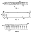
- an illumination source 10 that can be used with the illumination system described here contains an array 20 of one or more light sources 30 such as light emitting diodes (LEDs), flat fluorescent lamps, electroluminescent sources, or some other planar source suitable to the application embedded in a substrate 40 of highly reflective diffuse material.
- the illumination source 10 may be coupled to a waveguide as shown by the end views of the two illumination sources 10 adjacent the waveguide 50 in Figure 2.
- the arrows 60 represent the dispersion of light rays received from the illumination source 10 within the waveguide 50.
- the light sources 30 constitute a fraction of the total surface area of the substrate 40, ranging from about 10% to about 70%, and preferably from about 10% to about 30%.
- the light sources 30 could be configured in other layouts such as the two-dimensional array 70 of Figure 3.
- Other shapes and configurations may be utilized (e.g., triangular, circular, hexagonal, etc.), as will readily occur to those skilled in the art.
- 5 mm spacing has been successfully employed, the spacing can range from about 0.25 millimeters to about 3 centimeters, depending on the brightness of the light source employed.
- the light sources can be mounted on any suitable surface such as a copper-coated, glass-fiber board and spaced apart to achieve the desired luminance.
- a copper-coated, glass-fiber board and spaced apart to achieve the desired luminance.
- other mounting structures such as diamond or sapphire film can be used, as will readily occur to those skilled in the art.
- the light sources 30 are affixed to an underlying board by soldering or some other suitable means as will readily occur to those skilled in the art.
- the substrate 40 is then provided with openings that conform to the outline of the light sources 30, allowing the light emitted by the light sources 30 to pass through the substrate 40.
- the light sources 30 could be placed on top of the substrate 40 and the electrical connections brought through.
- LEDs having a size of approximately one millimeter square may be employed as the light sources, although other types and sizes of LEDs could be selected, as will be readily apparent to those skilled in the art. Suitable LEDs are commercially available from Dialight Corporation of Manasquan, N.J., Hewlett-Packard, and Nichia Chemical. Depending on the application, light sources of a single color (e.g., red, green, yellow, blue) or of multiple colors may be employed.
- the substrate 40 must have sufficient depth.
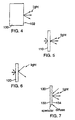
- Materials exhibiting a very high reflectance, i.e., approaching 100%, for visible light consist of diffuse scattering media with little or no absorption in the visible range.
- One example of a substrate having sufficient depth is the thick layer 100 of reflective diffuse material shown in the schematic cross-sectional diagram of Figure 4. Where the thickness of the layer 100 of diffuse material is about 0.51 mm or greater, at least about 95% of the light is reflected at the surface 102.
- the material is not sufficiently thick, a portion of the light energy will pass through the layer rather than be reflected.
- the reflectance for diffuse materials is low, typically less than 90%.
- the relatively thin layer 110 of reflective diffuse material of Figure 5 thus reflects a smaller percentage of the incident light rays.
- the specular material of the thin reflective layer 120 of Figure 6 will reflect approximately 80-95% of the incident light rays, it behaves like a mirror, and therefore diffuse material is preferred as it scatters the incident light rays.
- the composite reflector 130 shown in Figure 7 having a thin specular backing layer 132 behind a thin diffuse scattering layer 134.
- the two layers 132 and 134 may be joined by simply placing them together, relying on surface tension, bonding, adhesion, or lamination, the latter being the preferred method of joining the two layers.
- the specular layer 132 can be sputtered onto the diffuse layer 134 or provided as a coating on the diffuse layer 134.
- specular layer 132 behind a diffuse layer 134 The benefit of providing a specular layer 132 behind a diffuse layer 134 is realized whenever the thickness of the diffuse layer 134 is less about 0.5 mm. In such instances, depending on the specific materials employed, the addition of the specular layer 132 layer can increase the reflectance to at least about 97%.
- a composite reflector 130 having an 0.2 mm thick diffuse layer of PTFE material and a 0.076 mm thick specular layer of silver film provided comparable results.
- the thickness of the specular layer 132 layer may range from about 0.25 ⁇ m to about 0.1 mm, depending on the materials used and the method of manufacture (e.g., sputtering).
- the composite reflector 130 of Figure 7 may be employed in place of the substrate 40 in the illumination source 10 of Figures 1 and 2, resulting in a decrease of the physical depth required for the substrate when compared to substrates that are purely diffuse.
- Diffuse materials suitable for the applications discussed here are Spectralon from Labsphere, Inc. and PTFE (Teflon) film from Furon or E.I. du Pont de Nemours & Co.
- Specular materials include SilverluxTM, a product of 3M, and other highly-reflective (i.e., greater than 90% reflectance) materials such as aluminum, gold, and silver, as well as others as will readily occur to those skilled in the art.
- the reflectivity of any of the materials discussed may be measured using several commercially available instruments such as the Macbeth #7100 Spectrophotometer, New Windsor, N.Y,. or a Perkin Elmer #330 Spectrophotometer, Danbury, CT.
- the specular materials may be deposited on a secondary surface or directly on the diffuse material by such techniques as chemical vapor deposition, electron beam vapor deposition, sputtering, and the like.
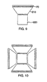
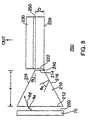
- the output of the illumination source 70 of Figure 3 may be used in an illumination system by coupling the light through a tapered coupling waveguide.
- an illumination source 70 having a two-dimensional array of light sources is positioned adjacent the input surface 212 of a tapered coupling waveguide 210.
- the output waveguide 220 provides light energy to a light collimating assembly 230.
- the drawing in Figure 8 is not drawn to scale; the actual relative dimensions may vary depending on the application.
- the layer 240 can be made from any optically clear material having an index of refraction preferably substantially equal to that of the waveguides 210 and 220.
- the two waveguides 210 and 220 may be thermally fused or fused by a solvent using materials and techniques well known in the art.
- adhesion layers may be employed between other components of the illumination system 200, e.g., between the output waveguide 220 and the light collimating assembly 230.
- a similar adhesion layer 250 is provided between the output waveguide 220 and the light collimating assembly 230. Again, the output waveguide 220 and the light collimating assembly 230 may be thermally fused or fused by a solvent.
- an air gap 260 is provided to maximize refraction of the light as it enters the tapered coupling waveguide 210.
- the air gap 260 is at least several wavelength in thickness, to permit refraction of the light travelling from the illumination source 70 into the tapered coupling waveguide 210.
- the waveguides 210 and 220 and associated structure, including the adhesion layers may be fabricated according to the methods and using such materials as polycarbonate, acrylic, polystyrene, glass, transparent ceramics, and a monomer mixture disclosed in U.S. Patent No. 5,396,350, issued March 7, 1995, to Beeson et al., for a Backlighting Apparatus Employing an Array of Microprisms, U.S. Patent No. 5,448,468, issued June 27, 1995, to Zimmerman et al., for an Illumination System Employing an Array of Microprisms, U.S. Patent No.
- the thickness D of the output waveguide 220 is kept small to maximize the number of reflections or bounces of light that enters from the output surface 214.
- the thickness D may range from about 0.5 to about 10 mm; typically, thicknesses from about 6 to about 8 mm have been employed. If light enters only through one edge, one may wish to provide a slight taper in the output waveguide 220 on the surface away from the collimating assembly 230 to optimize the number of bounces and therefore enhance the throughput of the output waveguide.
- the angle of taper may range from about 0.25° to about 2.0°; the actual angle is dependent on the length of the waveguide 220.
- TIR total internal reflection
- ⁇ c sin -1 ( n 1 / n 2 ), normal to the tapered surface 216, and where n 2 is the index of refraction of the tapered coupling waveguide 210 and n 1 is the index of refraction of the material (e.g., air) outside of the tapered coupling waveguide 210.
- the taper angle ⁇ t must be minimized as much as possible while still providing an input surface 212 of sufficient area.
- the designer must consider the angular distribution ( ⁇ ⁇ d ) of the output of the light sources, the indices of refraction of the tapered coupling waveguide 210 and the surrounding medium, and the maximum acceptable light loss.
- the taper angle ⁇ t can be derived from Snell's Law and the equation for the critical angle.
- the LEDs have an output of ⁇ d .
- ⁇ d' sin -1 ( n 1 / n 2 sin ⁇ d ).
- Light rays at the extreme angle ⁇ d' impact a tapered surface 216 at an incident angle of 90° - ( ⁇ t + ⁇ d' ) from the normal (with respect to the tapered surface 216).
- the rays then impact the opposite tapered surface 216 at an incident angle of 90° - (2 ⁇ t + ⁇ d' ) from the normal (with respect to the other tapered surface 216). In both cases, the incident angle must be greater than the critical angle to reflect.
- ⁇ i 90° - [(2( r -1) + 1) ⁇ t + ⁇ d' ] where r is the number of reflections of the light rays.
- ⁇ t must be selected such that ⁇ i > ⁇ c or 90° - [(2( r -1) + 1) ⁇ t + ⁇ d' ] > sin -1 ( n 1 / n 2 ) Solving for ⁇ t , ⁇ t ⁇ [90° - ⁇ d' - sin -1 ( n 1 / n 2 )]/[2( r -1) + 1)].
- a taper angle can be selected based on the LEDs employed, the relative index of refraction, and the number of reflections that will occur.
- the size of the input surface can be enlarged to the point where a certain portion of the outer extremities of the LED radiation pattern is forfeited.
- TIR keeps the majority of the light rays in the tapered coupling waveguide 210 and channels it to the output waveguide 220.
- the illumination system 200 is shown again in the plan view diagram of Figure 9.
- the tapered coupling waveguides 210 can be tapered in more than one direction, e.g., in both the x and y directions.
- the distribution angle of the LEDs can be minimized by placing converging lenses over each LED. Such lenses are typically provided by the manufacturer of the LEDs; in some instances, the lenses are an integral part of the LED package.
- the tapered coupling waveguide 210 could be a hollow structure having mirrored specular surfaces for achieving reflection within the waveguide 210.
- the surfaces can be fabricated through a coating process or a sputtering process, or some other method as will readily occur to one skilled in the art.
- a commercially-available tapered fiber-optic bundle could be substituted for the solid or hollow tapered coupling waveguide 210.
- this invention is applicable to a wide variety of devices such as direct illumination devices including lighting for commercial, office, residential, outdoor, automotive, and appliance applications.
- the invention may also be applied to displays for computer, automotive, military, aerospace, consumer, commercial, and industrial applications, and any other device requiring improved reflective materials to obtain an efficient illumination source.
Claims (6)
- Source d'éclairement (10), comprenant :un substrat (40) de matière réfléchissante ; etau moins une source de lumière planaire (30) fixée au substrat ; caractérisée en ce que le substrat (40) comprend une première couche (134) de matière réfléchissante diffuse, et une deuxième couche (132) de matière réfléchissante spéculaire, adjacente à la première couche.
- Système d'éclairement, comprenant :une source d'éclairement (10) selon la revendication 1,un guide d'onde (50) ayant une surface de sortie et au moins une surface d'entrée par le bord généralement perpendiculaire à la surface de sortie, où la surface d'entrée par le bord est adjacente à la source d'éclairement.
- Système d'éclairement selon la revendication 2, dans lequel la source de lumière (30) est une diode électroluminescente, une lampe fluorescente plate ou une source électroluminescente.
- Système d'éclairement, comprenant :une source d'éclairement (10) selon la revendication 1 ;un guide d'onde de sortie généralement planaire (220), le guide d'onde de sortie ayant une surface de sortie et au moins une surface d'entrée par le bord généralement perpendiculaire à la surface de sortie, où la surface d'entrée par le bord a une superficie substantiellement inférieure à la superficie du substrat (40) de la source d'éclairement ; etun guide d'onde de couplage effilé (210) pour coupler la sortie de la source d'éclairement à la surface d'entrée par le bord du guide d'onde de sortie, le guide d'onde de couplage comprenant une surface d'entrée pour accepter la sortie de la source d'éclairement, la surface d'entrée ayant une superficie approximativement égale et symétrique à au moins une partie du substrat de la source d'éclairement et une surface de sortie pour fournir une lumière à la surface d'entrée par le bord du guide d'onde de sortie, la surface de sortie ayant une superficie approximativement égale et symétrique par rapport à au moins une partie de la superficie de la surface d'entrée par le bord du guide d'onde de sortie.
- Système d'éclairement selon la revendication 2, 3 ou 4, dans lequel une pluralité de sources de lumière (30) est disposée en un réseau bidimensionnel.
- Système d'éclairement, comprenant :une source d'éclairement (10) selon la revendication 1 et comprenant en outre une pluralité de diodes électroluminescentes intégrées dans le substrat (40) et disposées en un réseau bidimensionnel;un guide d'onde de sortie généralement planaire (220), le guide d'onde de sortie ayant une surface de sortie et au moins une surface d'entrée par le bord généralement perpendiculaire à la surface de sortie, où la surface d'entrée par le bord a une superficie substantiellement inférieure à la superficie du substrat de la source d'éclairement ; etun guide d'onde de couplage effilé (210) pour coupler la lumière de la source d'éclairement à la surface d'entrée par le bord du guide d'onde de sortie, le guide d'onde de couplage comprenant une surface d'entrée pour accepter la sortie de la source d'éclairement, la surface d'entrée ayant une superficie approximativement de mêmes dimensions et symétrique par rapport à la superficie du substrat de la source d'éclairement ; etune surface de sortie pour fournir une lumière à la surface d'entrée par le bord du guide d'onde de sortie, la surface de sortie ayant une superficie approximativement de mêmes dimensions et symétrique par rapport à la superficie de la surface d'entrée par le bord du guide d'onde de sortie.
Applications Claiming Priority (3)
| Application Number | Priority Date | Filing Date | Title |
|---|---|---|---|
| US08/679,047 US6164789A (en) | 1996-07-12 | 1996-07-12 | Illumination sources and systems |
| US679047 | 1996-07-12 | ||
| PCT/US1997/011378 WO1998002690A1 (fr) | 1996-07-12 | 1997-07-01 | Sources et systemes d'eclairage |
Publications (2)
| Publication Number | Publication Date |
|---|---|
| EP1012500A1 EP1012500A1 (fr) | 2000-06-28 |
| EP1012500B1 true EP1012500B1 (fr) | 2003-04-02 |
Family
ID=24725368
Family Applications (1)
| Application Number | Title | Priority Date | Filing Date |
|---|---|---|---|
| EP97932394A Expired - Lifetime EP1012500B1 (fr) | 1996-07-12 | 1997-07-01 | Sources et systemes d'eclairage |
Country Status (8)
| Country | Link |
|---|---|
| US (1) | US6164789A (fr) |
| EP (1) | EP1012500B1 (fr) |
| JP (2) | JP4031533B2 (fr) |
| KR (1) | KR100492859B1 (fr) |
| AT (1) | ATE236377T1 (fr) |
| DE (1) | DE69720549T2 (fr) |
| TW (1) | TW384402B (fr) |
| WO (1) | WO1998002690A1 (fr) |
Families Citing this family (40)
| Publication number | Priority date | Publication date | Assignee | Title |
|---|---|---|---|---|
| JP3585097B2 (ja) * | 1998-06-04 | 2004-11-04 | セイコーエプソン株式会社 | 光源装置,光学装置および液晶表示装置 |
| JP4656444B2 (ja) * | 1998-06-04 | 2011-03-23 | セイコーエプソン株式会社 | プロジェクタ |
| CH690247A5 (de) * | 1999-03-24 | 2000-06-15 | Gerhard Staufert | Leuchtkörperaufbau. |
| JP4049486B2 (ja) * | 1999-08-11 | 2008-02-20 | 三洋電機株式会社 | ショーケース |
| US7027691B1 (en) * | 1999-10-05 | 2006-04-11 | Visteon Global Technologies, Inc. | Light coupling and distribution system |
| JP2001184927A (ja) * | 1999-12-28 | 2001-07-06 | Minebea Co Ltd | 面状照明装置 |
| US6869427B1 (en) * | 2000-06-15 | 2005-03-22 | Kamran K. Shokoohi | LED fixation device for topical anesthesia eye surgery |
| US6663262B2 (en) * | 2001-09-10 | 2003-12-16 | 3M Innovative Properties Company | Backlighting transmissive displays |
| JP2004095390A (ja) * | 2002-08-30 | 2004-03-25 | Fujitsu Display Technologies Corp | 照明装置及び表示装置 |
| JP4216577B2 (ja) * | 2002-12-20 | 2009-01-28 | シチズン電子株式会社 | 導光板 |
| US20090185392A1 (en) * | 2003-03-26 | 2009-07-23 | Optim, Inc. | Detachable illumination system |
| JP4379786B2 (ja) * | 2003-11-11 | 2009-12-09 | 株式会社エンプラス | 面光源装置 |
| JP4042687B2 (ja) * | 2003-12-15 | 2008-02-06 | ソニー株式会社 | 照明装置及びバックライト装置 |
| US20050136200A1 (en) * | 2003-12-19 | 2005-06-23 | Durell Christopher N. | Diffuse high reflectance film |
| US7591563B2 (en) * | 2004-01-15 | 2009-09-22 | Au Optronics Corporation | Backlight device for display system providing enhanced peripheral illumination |
| DE102004012541A1 (de) * | 2004-03-15 | 2005-10-06 | BSH Bosch und Siemens Hausgeräte GmbH | Leuchtmodul zur Montage in einem Haushaltgerät und Haushaltgerät mit einem solchen |
| TW200602585A (en) * | 2004-03-16 | 2006-01-16 | Koninkl Philips Electronics Nv | High brightness illumination device with incoherent solid state light source |
| KR100649162B1 (ko) * | 2004-10-14 | 2006-11-28 | 주식회사 삼성산업 | Mspc 제품용 몰드의 탈형 방법 |
| KR100665707B1 (ko) * | 2004-12-13 | 2007-01-09 | 주식회사 보림에쓰에쓰 | Mspc 조성물 타설 방법 |
| US7296916B2 (en) * | 2004-12-21 | 2007-11-20 | 3M Innovative Properties Company | Illumination assembly and method of making same |
| US7285802B2 (en) * | 2004-12-21 | 2007-10-23 | 3M Innovative Properties Company | Illumination assembly and method of making same |
| US20060131601A1 (en) * | 2004-12-21 | 2006-06-22 | Ouderkirk Andrew J | Illumination assembly and method of making same |
| JP4442766B2 (ja) * | 2005-02-18 | 2010-03-31 | 株式会社エンプラス | 導光板、面光源装置及び表示装置 |
| US20060243379A1 (en) * | 2005-04-29 | 2006-11-02 | E-Beam & Light, Inc. | Method and apparatus for lamination by electron beam irradiation |
| US7360905B2 (en) * | 2005-06-24 | 2008-04-22 | Texas Instruments Incorporated | Compact optical engine for very small personal projectors using LED illumination |
| TW200722850A (en) * | 2005-12-02 | 2007-06-16 | Innolux Display Corp | Backlight module and liquid crystal display device |
| KR100770602B1 (ko) * | 2005-12-30 | 2007-10-29 | 서울반도체 주식회사 | 광가이드 디바이스 및 이를 포함하는 lcd용 백라이팅모듈 |
| US7926995B2 (en) * | 2006-10-02 | 2011-04-19 | Asahi Kasei Kabushiki Kaisha | Backlight assembly with thin film light pipe |
| TWI330240B (en) * | 2006-11-03 | 2010-09-11 | Chimei Innolux Corp | Light emitting diode and backlight module using the same |
| US8662727B2 (en) * | 2008-03-19 | 2014-03-04 | I2Ic Corporation | Apparatus for efficiently coupling light from a light source into a thin object |
| WO2010049912A2 (fr) * | 2008-10-31 | 2010-05-06 | Udayan Kanade | Source de lumière avec mécanisme de récupération de lumière |
| US8882328B2 (en) * | 2008-11-24 | 2014-11-11 | 3M Innovative Properties Company | Input edge coupler having taper region |
| EP2320125A1 (fr) | 2009-11-04 | 2011-05-11 | Koninklijke Philips Electronics N.V. | Dispositif d'éclairage |
| US8845171B2 (en) * | 2011-05-19 | 2014-09-30 | Shenzhen China Star Optoelectronics Technology Co., Ltd. | LED light-source structure and backlight module |
| CN103827572B (zh) * | 2011-09-15 | 2017-02-15 | 三菱电机株式会社 | 光强度分布转换元件、面光源装置和液晶显示装置 |
| CN104238186A (zh) * | 2013-06-20 | 2014-12-24 | 扬升照明股份有限公司 | 背光模块 |
| DE102015206298B3 (de) * | 2015-04-09 | 2016-08-11 | BSH Hausgeräte GmbH | Wäschepflegegerät mit einem Beleuchtungselement |
| US9823411B2 (en) | 2015-09-25 | 2017-11-21 | Snaptrack Inc. | Etendue-preserving light coupling system having light output aperture smaller than light input aperture |
| TW201903444A (zh) * | 2017-04-21 | 2019-01-16 | 美商康寧公司 | 光耦合器 |
| US20190041050A1 (en) | 2017-08-01 | 2019-02-07 | Technical Consumer Products, Inc. | Edge-lit light fixture having capabilities for a secondary service |
Family Cites Families (13)
| Publication number | Priority date | Publication date | Assignee | Title |
|---|---|---|---|---|
| US33722A (en) * | 1861-11-12 | Improved mode of treating drying-oils for manufacture of varnish and other purposes | ||
| JPS61188509A (ja) * | 1985-02-16 | 1986-08-22 | Nippon Hoso Kyokai <Nhk> | 光結合装置 |
| USRE33722E (en) * | 1987-04-28 | 1991-10-22 | Spectra Diode Laboratories, Inc. | Optical system with bright light output |
| US4935665A (en) * | 1987-12-24 | 1990-06-19 | Mitsubishi Cable Industries Ltd. | Light emitting diode lamp |
| JP2730310B2 (ja) * | 1991-02-21 | 1998-03-25 | 東ソー株式会社 | パネル用バックライト |
| DE69212662T2 (de) * | 1991-02-21 | 1997-02-20 | Tosoh Corp | Vorrichtung zur Hinterbeleuchtung |
| JPH0545652U (ja) * | 1991-11-21 | 1993-06-18 | 信越ポリマー株式会社 | 面状光源装置 |
| JPH0715045A (ja) * | 1992-05-11 | 1995-01-17 | Susumu Kurokawa | 面発光照明装置 |
| US5481385A (en) * | 1993-07-01 | 1996-01-02 | Alliedsignal Inc. | Direct view display device with array of tapered waveguide on viewer side |
| US5396350A (en) * | 1993-11-05 | 1995-03-07 | Alliedsignal Inc. | Backlighting apparatus employing an array of microprisms |
| US5428468A (en) * | 1993-11-05 | 1995-06-27 | Alliedsignal Inc. | Illumination system employing an array of microprisms |
| US5462700A (en) * | 1993-11-08 | 1995-10-31 | Alliedsignal Inc. | Process for making an array of tapered photopolymerized waveguides |
| US5613751A (en) * | 1995-06-27 | 1997-03-25 | Lumitex, Inc. | Light emitting panel assemblies |
-
1996
- 1996-07-12 US US08/679,047 patent/US6164789A/en not_active Expired - Lifetime
-
1997
- 1997-06-30 TW TW086109181A patent/TW384402B/zh not_active IP Right Cessation
- 1997-07-01 JP JP50605598A patent/JP4031533B2/ja not_active Expired - Lifetime
- 1997-07-01 AT AT97932394T patent/ATE236377T1/de not_active IP Right Cessation
- 1997-07-01 WO PCT/US1997/011378 patent/WO1998002690A1/fr active IP Right Grant
- 1997-07-01 KR KR10-1999-7000214A patent/KR100492859B1/ko not_active IP Right Cessation
- 1997-07-01 EP EP97932394A patent/EP1012500B1/fr not_active Expired - Lifetime
- 1997-07-01 DE DE69720549T patent/DE69720549T2/de not_active Expired - Lifetime
-
2007
- 2007-08-16 JP JP2007212150A patent/JP2008004558A/ja active Pending
Also Published As
| Publication number | Publication date |
|---|---|
| ATE236377T1 (de) | 2003-04-15 |
| US6164789A (en) | 2000-12-26 |
| JP2000514949A (ja) | 2000-11-07 |
| KR20000023750A (ko) | 2000-04-25 |
| KR100492859B1 (ko) | 2005-05-31 |
| JP2008004558A (ja) | 2008-01-10 |
| DE69720549D1 (de) | 2003-05-08 |
| JP4031533B2 (ja) | 2008-01-09 |
| DE69720549T2 (de) | 2003-12-24 |
| EP1012500A1 (fr) | 2000-06-28 |
| WO1998002690A1 (fr) | 1998-01-22 |
| TW384402B (en) | 2000-03-11 |
Similar Documents
| Publication | Publication Date | Title |
|---|---|---|
| EP1012500B1 (fr) | Sources et systemes d'eclairage | |
| JP4087864B2 (ja) | 平面発光装置 | |
| EP2284437B1 (fr) | Dispositif transréflectif et afficheur à dispositif transréflectif | |
| US6824285B2 (en) | Light source and liquid crystal display device using this light source | |
| US7168841B2 (en) | Backlight module having independent light source | |
| CN101438426B (zh) | 带有会聚光学元件的led封装 | |
| EP1437610B1 (fr) | Unité pour rétroéclairage | |
| US7085056B2 (en) | Light guide plate with diffraction gratings and backlight module using the same | |
| US7527416B2 (en) | Light guide plate with diffraction gratings and backlight module using the same | |
| US7309882B2 (en) | Surface light source with photonic crystal LED | |
| US20090067176A1 (en) | Backlight module and light guide plate thereof | |
| CN101095077A (zh) | 具有带凹入的棱锥形结构的结构化表面的光学薄膜 | |
| US5136479A (en) | Device and method for creating an areal light source | |
| JP2007535149A (ja) | 発光ダイオード用光学マニホールド | |
| JP2009523308A5 (fr) | ||
| EP1397610A1 (fr) | Systeme d'eclairage compact et dispositif d'affichage | |
| KR20040089892A (ko) | 광편향부재를 구비하는 도광판 및 측면 발광형 백라이트장치 | |
| CN111665591A (zh) | 一种导光板、背光模组和液晶显示模组 | |
| US20070041701A1 (en) | Light guide plate and a backlight system | |
| EP2223351B1 (fr) | Dispositif à émission latérale équipé d'un réflecteur supérieur hybride | |
| JP4389529B2 (ja) | 面照明装置及び導光板 | |
| CN100468165C (zh) | 发光二极管及采用该发光二极管的背光模组 | |
| US7242838B2 (en) | Backlight module with reflection member | |
| US7095942B2 (en) | Planar light device | |
| US7048399B2 (en) | Light guide plate and surface light source |
Legal Events
| Date | Code | Title | Description |
|---|---|---|---|
| PUAI | Public reference made under article 153(3) epc to a published international application that has entered the european phase |
Free format text: ORIGINAL CODE: 0009012 |
|
| 17P | Request for examination filed |
Effective date: 19990111 |
|
| AK | Designated contracting states |
Kind code of ref document: A1 Designated state(s): AT BE CH DE DK ES FI FR GB GR IE IT LI LU NL PT SE |
|
| RAP1 | Party data changed (applicant data changed or rights of an application transferred) |
Owner name: HONEYWELL INTERNATIONAL INC. |
|
| 17Q | First examination report despatched |
Effective date: 20020507 |
|
| GRAH | Despatch of communication of intention to grant a patent |
Free format text: ORIGINAL CODE: EPIDOS IGRA |
|
| GRAH | Despatch of communication of intention to grant a patent |
Free format text: ORIGINAL CODE: EPIDOS IGRA |
|
| GRAA | (expected) grant |
Free format text: ORIGINAL CODE: 0009210 |
|
| AK | Designated contracting states |
Designated state(s): AT BE CH DE DK ES FI FR GB GR IE IT LI LU NL PT SE |
|
| PG25 | Lapsed in a contracting state [announced via postgrant information from national office to epo] |
Ref country code: IT Free format text: LAPSE BECAUSE OF FAILURE TO SUBMIT A TRANSLATION OF THE DESCRIPTION OR TO PAY THE FEE WITHIN THE PRESCRIBED TIME-LIMIT;WARNING: LAPSES OF ITALIAN PATENTS WITH EFFECTIVE DATE BEFORE 2007 MAY HAVE OCCURRED AT ANY TIME BEFORE 2007. THE CORRECT EFFECTIVE DATE MAY BE DIFFERENT FROM THE ONE RECORDED. Effective date: 20030402 Ref country code: FI Free format text: LAPSE BECAUSE OF FAILURE TO SUBMIT A TRANSLATION OF THE DESCRIPTION OR TO PAY THE FEE WITHIN THE PRESCRIBED TIME-LIMIT Effective date: 20030402 |
|
| REG | Reference to a national code |
Ref country code: GB Ref legal event code: FG4D |
|
| REG | Reference to a national code |
Ref country code: CH Ref legal event code: EP |
|
| REG | Reference to a national code |
Ref country code: IE Ref legal event code: FG4D |
|
| REF | Corresponds to: |
Ref document number: 69720549 Country of ref document: DE Date of ref document: 20030508 Kind code of ref document: P |
|
| PG25 | Lapsed in a contracting state [announced via postgrant information from national office to epo] |
Ref country code: LU Free format text: LAPSE BECAUSE OF NON-PAYMENT OF DUE FEES Effective date: 20030701 Ref country code: IE Free format text: LAPSE BECAUSE OF NON-PAYMENT OF DUE FEES Effective date: 20030701 |
|
| PG25 | Lapsed in a contracting state [announced via postgrant information from national office to epo] |
Ref country code: SE Free format text: LAPSE BECAUSE OF FAILURE TO SUBMIT A TRANSLATION OF THE DESCRIPTION OR TO PAY THE FEE WITHIN THE PRESCRIBED TIME-LIMIT Effective date: 20030702 Ref country code: PT Free format text: LAPSE BECAUSE OF FAILURE TO SUBMIT A TRANSLATION OF THE DESCRIPTION OR TO PAY THE FEE WITHIN THE PRESCRIBED TIME-LIMIT Effective date: 20030702 Ref country code: GR Free format text: LAPSE BECAUSE OF FAILURE TO SUBMIT A TRANSLATION OF THE DESCRIPTION OR TO PAY THE FEE WITHIN THE PRESCRIBED TIME-LIMIT Effective date: 20030702 Ref country code: DK Free format text: LAPSE BECAUSE OF FAILURE TO SUBMIT A TRANSLATION OF THE DESCRIPTION OR TO PAY THE FEE WITHIN THE PRESCRIBED TIME-LIMIT Effective date: 20030702 |
|
| PG25 | Lapsed in a contracting state [announced via postgrant information from national office to epo] |
Ref country code: ES Free format text: LAPSE BECAUSE OF FAILURE TO SUBMIT A TRANSLATION OF THE DESCRIPTION OR TO PAY THE FEE WITHIN THE PRESCRIBED TIME-LIMIT Effective date: 20031030 |
|
| ET | Fr: translation filed | ||
| PLBE | No opposition filed within time limit |
Free format text: ORIGINAL CODE: 0009261 |
|
| STAA | Information on the status of an ep patent application or granted ep patent |
Free format text: STATUS: NO OPPOSITION FILED WITHIN TIME LIMIT |
|
| 26N | No opposition filed |
Effective date: 20040105 |
|
| REG | Reference to a national code |
Ref country code: IE Ref legal event code: MM4A |
|
| REG | Reference to a national code |
Ref country code: GB Ref legal event code: 732E Free format text: REGISTERED BETWEEN 20100708 AND 20100714 |
|
| PGFP | Annual fee paid to national office [announced via postgrant information from national office to epo] |
Ref country code: NL Payment date: 20100624 Year of fee payment: 14 Ref country code: CH Payment date: 20100726 Year of fee payment: 14 Ref country code: BE Payment date: 20100630 Year of fee payment: 14 |
|
| PGFP | Annual fee paid to national office [announced via postgrant information from national office to epo] |
Ref country code: AT Payment date: 20100616 Year of fee payment: 14 |
|
| REG | Reference to a national code |
Ref country code: NL Ref legal event code: SD Effective date: 20110415 |
|
| REG | Reference to a national code |
Ref country code: CH Ref legal event code: PUE Owner name: UBERGRAFF UGHIF GMBH.,LLC Free format text: HONEYWELL INTERNATIONAL INC.#101 COLUMBIA ROAD, P.O. BOX 2245#MORRISTOWN, NEW JERSEY 07962-2245 (US) -TRANSFER TO- UBERGRAFF UGHIF GMBH.,LLC#160 GREENTREE DRIVE, SUITE 101#DOVER DE 19904 (US) Ref country code: CH Ref legal event code: NV Representative=s name: ISLER & PEDRAZZINI AG |
|
| REG | Reference to a national code |
Ref country code: FR Ref legal event code: TP |
|
| BERE | Be: lapsed |
Owner name: *UBERGRAFF UGHIF GMBH LLC Effective date: 20110731 |
|
| REG | Reference to a national code |
Ref country code: NL Ref legal event code: V1 Effective date: 20120201 |
|
| REG | Reference to a national code |
Ref country code: CH Ref legal event code: PL |
|
| REG | Reference to a national code |
Ref country code: AT Ref legal event code: MM01 Ref document number: 236377 Country of ref document: AT Kind code of ref document: T Effective date: 20110701 |
|
| PG25 | Lapsed in a contracting state [announced via postgrant information from national office to epo] |
Ref country code: BE Free format text: LAPSE BECAUSE OF NON-PAYMENT OF DUE FEES Effective date: 20110731 Ref country code: LI Free format text: LAPSE BECAUSE OF NON-PAYMENT OF DUE FEES Effective date: 20110731 Ref country code: CH Free format text: LAPSE BECAUSE OF NON-PAYMENT OF DUE FEES Effective date: 20110731 |
|
| PG25 | Lapsed in a contracting state [announced via postgrant information from national office to epo] |
Ref country code: NL Free format text: LAPSE BECAUSE OF NON-PAYMENT OF DUE FEES Effective date: 20120201 |
|
| PG25 | Lapsed in a contracting state [announced via postgrant information from national office to epo] |
Ref country code: AT Free format text: LAPSE BECAUSE OF NON-PAYMENT OF DUE FEES Effective date: 20110701 |
|
| REG | Reference to a national code |
Ref country code: FR Ref legal event code: PLFP Year of fee payment: 19 |
|
| REG | Reference to a national code |
Ref country code: FR Ref legal event code: PLFP Year of fee payment: 20 |
|
| PGFP | Annual fee paid to national office [announced via postgrant information from national office to epo] |
Ref country code: GB Payment date: 20160624 Year of fee payment: 20 |
|
| PGFP | Annual fee paid to national office [announced via postgrant information from national office to epo] |
Ref country code: FR Payment date: 20160621 Year of fee payment: 20 |
|
| PGFP | Annual fee paid to national office [announced via postgrant information from national office to epo] |
Ref country code: DE Payment date: 20160801 Year of fee payment: 20 |
|
| REG | Reference to a national code |
Ref country code: DE Ref legal event code: R071 Ref document number: 69720549 Country of ref document: DE |
|
| REG | Reference to a national code |
Ref country code: GB Ref legal event code: PE20 Expiry date: 20170630 |
|
| PG25 | Lapsed in a contracting state [announced via postgrant information from national office to epo] |
Ref country code: GB Free format text: LAPSE BECAUSE OF EXPIRATION OF PROTECTION Effective date: 20170630 |