EP1011973B1 - Viewing and imaging systems - Google Patents
Viewing and imaging systemsInfo
- Publication number
- EP1011973B1 EP1011973B1 EP98910851A EP98910851A EP1011973B1 EP 1011973 B1 EP1011973 B1 EP 1011973B1 EP 98910851 A EP98910851 A EP 98910851A EP 98910851 A EP98910851 A EP 98910851A EP 1011973 B1 EP1011973 B1 EP 1011973B1
- Authority
- EP
- European Patent Office
- Prior art keywords
- lighting
- screen
- board
- lighting means
- light
- Prior art date
- Legal status (The legal status is an assumption and is not a legal conclusion. Google has not performed a legal analysis and makes no representation as to the accuracy of the status listed.)
- Expired - Lifetime
Links
- 238000003384 imaging method Methods 0.000 title claims description 19
- 238000000034 method Methods 0.000 claims description 13
- 230000004044 response Effects 0.000 claims description 5
- 230000002123 temporal effect Effects 0.000 claims description 5
- 108091006146 Channels Proteins 0.000 description 57
- 239000000523 sample Substances 0.000 description 26
- 239000012528 membrane Substances 0.000 description 9
- 230000001960 triggered effect Effects 0.000 description 9
- 230000003287 optical effect Effects 0.000 description 8
- 238000007689 inspection Methods 0.000 description 6
- 238000005286 illumination Methods 0.000 description 5
- 230000004888 barrier function Effects 0.000 description 3
- 229910000679 solder Inorganic materials 0.000 description 3
- 238000011109 contamination Methods 0.000 description 2
- 230000001419 dependent effect Effects 0.000 description 2
- 238000013461 design Methods 0.000 description 2
- 230000000694 effects Effects 0.000 description 2
- 230000008569 process Effects 0.000 description 2
- 238000012545 processing Methods 0.000 description 2
- 239000000758 substrate Substances 0.000 description 2
- 230000001360 synchronised effect Effects 0.000 description 2
- 238000012546 transfer Methods 0.000 description 2
- 230000003213 activating effect Effects 0.000 description 1
- 238000010586 diagram Methods 0.000 description 1
- 239000000284 extract Substances 0.000 description 1
- 230000008014 freezing Effects 0.000 description 1
- 238000007710 freezing Methods 0.000 description 1
- 238000004519 manufacturing process Methods 0.000 description 1
- 239000000463 material Substances 0.000 description 1
- 230000007246 mechanism Effects 0.000 description 1
- 238000012986 modification Methods 0.000 description 1
- 230000004048 modification Effects 0.000 description 1
- 238000012544 monitoring process Methods 0.000 description 1
- 238000001208 nuclear magnetic resonance pulse sequence Methods 0.000 description 1
- 239000004065 semiconductor Substances 0.000 description 1
- 238000012163 sequencing technique Methods 0.000 description 1
- 229910001220 stainless steel Inorganic materials 0.000 description 1
- 239000010935 stainless steel Substances 0.000 description 1
- 230000007704 transition Effects 0.000 description 1
Images



Classifications
-
- G—PHYSICS
- G03—PHOTOGRAPHY; CINEMATOGRAPHY; ANALOGOUS TECHNIQUES USING WAVES OTHER THAN OPTICAL WAVES; ELECTROGRAPHY; HOLOGRAPHY
- G03F—PHOTOMECHANICAL PRODUCTION OF TEXTURED OR PATTERNED SURFACES, e.g. FOR PRINTING, FOR PROCESSING OF SEMICONDUCTOR DEVICES; MATERIALS THEREFOR; ORIGINALS THEREFOR; APPARATUS SPECIALLY ADAPTED THEREFOR
- G03F9/00—Registration or positioning of originals, masks, frames, photographic sheets or textured or patterned surfaces, e.g. automatically
-
- H—ELECTRICITY
- H05—ELECTRIC TECHNIQUES NOT OTHERWISE PROVIDED FOR
- H05K—PRINTED CIRCUITS; CASINGS OR CONSTRUCTIONAL DETAILS OF ELECTRIC APPARATUS; MANUFACTURE OF ASSEMBLAGES OF ELECTRICAL COMPONENTS
- H05K1/00—Printed circuits
- H05K1/02—Details
- H05K1/0266—Marks, test patterns or identification means
-
- H—ELECTRICITY
- H05—ELECTRIC TECHNIQUES NOT OTHERWISE PROVIDED FOR
- H05K—PRINTED CIRCUITS; CASINGS OR CONSTRUCTIONAL DETAILS OF ELECTRIC APPARATUS; MANUFACTURE OF ASSEMBLAGES OF ELECTRICAL COMPONENTS
- H05K3/00—Apparatus or processes for manufacturing printed circuits
- H05K3/10—Apparatus or processes for manufacturing printed circuits in which conductive material is applied to the insulating support in such a manner as to form the desired conductive pattern
- H05K3/12—Apparatus or processes for manufacturing printed circuits in which conductive material is applied to the insulating support in such a manner as to form the desired conductive pattern using thick film techniques, e.g. printing techniques to apply the conductive material or similar techniques for applying conductive paste or ink patterns
- H05K3/1216—Apparatus or processes for manufacturing printed circuits in which conductive material is applied to the insulating support in such a manner as to form the desired conductive pattern using thick film techniques, e.g. printing techniques to apply the conductive material or similar techniques for applying conductive paste or ink patterns by screen printing or stencil printing
Definitions
- This invention relates to imaging systems for particular though not exclusive application in the field of screen printers for applying solder paste to printed circuit boards.
- the following description will focus on screen printer applications, but it will be understood that the various aspects of the invention find application in other areas where similar techniques are used.
- the screen In screen printers for pcb's, the screen is positioned over the circuit board and solder paste is applied to the board through apertures in the screen. To ensure that the solder paste is printed at the correct locations on the board for subsequent component placement, the screen must be aligned with the board prior to printing.
- an imaging device such as a video probe is generally moved between the screen and board to view reference marks, or "fiducials", at corresponding positions on the screen and board. Images of corresponding fiducials on the screen and board are relayed to vision processing apparatus.
- the vision processing apparatus determines the relative mis-alignment of the screen and board from the positions of the fiducials in the acquired images, and the relative position of the screen and board is adjusted to achieve alignment to prior to printing.
- FIG. 1 of the accompanying drawings The general arrangement of one type of screen printer is illustrated in Figure 1 of the accompanying drawings.
- the circuit board 1 to be printed is supported by a base (not shown) of the printer in a generally horizontal plane parallel to the x and y axes shown in the figure.
- a screen 2 is supported in a frame 2a so as to lie above. and generally parallel to. the board 1.
- the position of the screen 2 in the xy plane can be adjusted by means of screen positioning motors 3 the operation of which is controlled by a position controller 4.
- the support frame 2a and screen positioning motors 3 are mounted in a printhead portion (not shown) of the printer which can be pivoted away from the base to allow access when necessary, for example to adjust the board support.
- the apparatus includes an imaging device 5 which is mounted on an XY table (not shown) for movement in a horizontal plane between the board 1 and screen 2. The position of the imaging device 5 is also controlled by the position controller 4.
- the surface of the screen 2 facing the board 1 has a plurality of reference marks, or screen fiducials, 6a and 6b thereon.
- the surface of the board 1 facing the screen 2 has corresponding board fiducials 7a and 7b.
- the positions of the board and screen fiducials are such that when each pair of corresponding fiducials 6a, 7a and 6b, 7b are in alignment, the screen is correctly aligned relative to the board for the subsequent printing operation to be performed after simply raising the board into contact with the screen by means of a mechanism provided in the base of the printer.
- the imaging device 5 is operated so as to acquire images of the fiducials 6, 7 and the acquired images are supplied to a vision processor 8 which is programmed to determine the locations of the fiducials in the images.
- the fiducial location data is then supplied to the position controller 4 for adjusting the position of the screen 2 to bring the corresponding fiducials 6a, 7a and 6b, 7b, and hence the board and screen, into alignment.
- a video monitor 9a allows an operator to monitor images supplied to the vision processor 8.
- An operator interface 9b is connected to the position controller 4 to allow operator control of the apparatus, eg. during preliminary set up procedures.
- the general arrangement of a known imaging device 5 is illustrated schematically in Figure 2 of the drawings.
- the imaging device is a video probe comprising a CCD camera 11 and an optical system indicated generally at 12.
- the optical system 12 comprises screen and board lighting indicated schematically at 13 and 14 respectively.
- the screen and board lighting 13 and 14 constitutes "direct lighting" for illuminating the regions A and B of the screen and board with substantially collimated light as indicated by the arrows in the figure.
- the direct lighting 13, 14 can be implemented in a number of ways, for example by optical arrangements which receive light from sources at one side thereof and reflect the light upwardly/downwardly towards the screen/board.
- the reflecting means 16 may be, for example, a prism arrangement which reflects incident light from the screen/board along the return light channel 17.
- the return light is transmitted along the channel 17 via various optics (not shown) to the CCD camera 11.
- the illuminated regions of the screen and board may be imaged side by side on the CCD array.
- the direct light which is nominally perpendicular to the screen and board, is sufficient for viewing fiducials for alignment purposes
- the probe 5 is also to be used for inspection purposes then it is desirable for additional, diffuse lighting to be provided.
- the direct light may be insufficient to enable the required features to be distinguished.
- the location of the direct screen and board lighting 13, 14 above and below the return light channel 17 as shown in Figure 2 means that in practice there is inadequate space to provide the required diffuse lighting on the probe if a practical compact design is to be achieved.
- DE-A-4233455 discloses a registration method and apparatus for registering a printing screen with a print object. In performing this registration, the printing screen and the print object are illuminated, and a reference mark on the printing screen and a registration hole in the print object imaged.
- WO-A-98/07569 which is state of the art under Article 54(3), discloses a video probe which is used to view a printing screen and a substrate prior to printing to provide image signals which are utilised to align the printing screen and the substrate prior to printing.
- the present invention provides an imaging apparatus for acquiring images of regions, in particular of a screen and/or board in a screen printer, the apparatus comprising: a plurality of lighting means for illuminating regions to be imaged; and imaging means for acquiring images of the regions illuminated by the lighting means; characterized in that: the apparatus further comprises control means for controlling each lighting means to generate a pulse of light, wherein the control means is operable to control the plurality of lighting means to generate respective pulses of different durations such that the temporal midpoints of pulses from respective lighting means are coincident.
- the imaging device can include a plurality of lighting means which can generate pulses of different durations, i.e. different temporal pulse widths, but though the pulse widths for different lighting means are different, the pulses are centred at the same point in time. Since the effective intensity of light from different lighting means is dependent on the pulse width, this allows the various lighting means to produce different intensity light in a strobe situation, the coincident light pulses "freezing" the image at a single point in time.
- the plurality of lighting means may comprise direct lighting means and/or diffuse lighting means such as may be used for inspection purposes.
- control means is operable to vary the pulse duration, and hence effective intensity, of one or more, and preferably all, of the lighting means in response to a control input.
- the intensity of individual lighting means can be varied independently of the others, while the light pulses from different sources are still centred on the same point in time by the control means.
- the control means may be operable in a first mode to control the lighting means to generate light pulses repeatedly, preferably in synchronism with a video signal output by the imaging means, and most preferably at the frame rate of the video signal.
- the control means may also be operable in a second mode to trigger the lighting means to generate pulses at times dependent on external control signals received from the control means.
- the present invention provides a method of acquiring images of regions, in particular of a screen and/or board in a screen printer, the method comprising the steps of: illuminating regions to be imaged by a plurality of lighting means; and acquiring images of the regions illuminated by the lighting means; characterized in that: the step of illuminating regions to be imaged comprises the step of operating a plurality of lighting means to generate respective pulses of light for illuminating the regions to be imaged; and the method further comprises the step of controlling the plurality of lighting means to generate respective pulses of different durations such that the temporal midpoints of pulses from respective lighting means are coincident.
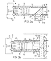
- Figures 3a, 3b and 3c are schematic views; partially cut away, of an imaging device in the form of a video probe 20 embodying the invention.
- Figure 3a is a plan view of the probe with the top cut away to illustrate the viewing apparatus.
- Figure 3b is a schematic cross-section along line A-A of Figure 3a showing a side view of the probe.
- Figure 3c is a schematic cross-section along line B-B of Figure 3a showing an end view of the probe.
- the probe 20 is shown located between a screen 2 and board 1 to be viewed.
- the probe 20 comprises a CCD camera 21 and viewing apparatus indicated generally at 22 for illuminating and viewing regions of the screen 2 and board I to be imaged.
- the CCD 21 is connected to the vision processor 8 ( Figure 1) to supply video images thereto and to receive control signals from the vision processor and operator interface 9b ( Figure 1).
- the viewing apparatus 22 comprises a housing 23 defining a return light channel 24 containing a lens system 25 which focuses return light via telecentric stop 26 onto the imaging plane of the CCD 21.
- the return light channel 24 also contains a beamsplitting plate 27 and a roof prism 28 arranged as shown in the figures.
- the roof prism 28 is located between apertures 29 and 30 in the housing 23 for passage of light between the roof prism and the screen and board respectively.
- lighting means is mounted on one side of the return light channel 24.
- the lighting means 32 provides the direct lighting for the screen and board.
- the direct lighting means 32 comprises screen and board LEDs, 33 and 34 respectively, between which is mounted a further roof prism 35.
- Upper and lower collimating lenses 36 and 37 are located adjacent the roof prism 35.
- a light barrier in the form of a thin membrane 39 extends between the point of the roof prism 35, the beamsplitting plate 27 and the point of the roof prism 28.
- the membrane 39 may be any suitable light barrier, for example a thin stainless steel sheet which is blackened to minimise reflections.
- the membrane 39 is aligned with the optical axis O of the return light channel 27 in a plane substantially parallel to the screen and board.
- additional lighting is provided adjacent the apertures 29, 30 in the housing 23.
- two rings of LEDs 40a and 40b are provided around the aperture 29, the LEDs in each ring being angled so as to point generally towards the screen field of view.
- the inner ring 40a may comprise 12 LEDs in total
- the outer ring 40b may comprise 16 LEDs in total.
- two rings of LEDs 41a and 41b are provided on the board side adjacent the aperture 30.
- the LEDs 40a and 40b provide diffuse lighting for illuminating the screen 2 with light from many different directions, and the LEDs 41a, 41b similarly provide diffuse lighting for the board 1.
- the LEDs 40a and 40b are mounted on a lighting control circuit board 43 on which control and drive circuitry for the LEDs is provided as discussed further below.
- the LEDs 41a and 41b are mounted on a lighting control board 44. Suitable connections (not shown) are provided between the lighting control boards 43, 44 and the CCD 21 to allow control of the diffuse lighting by the camera 21, vision processor 8 and operator interface 9b ( Figure 1).
- the direct lighting LEDs 33, 34 are also connected to the lighting control boards 43, 44 for control thereby.
- the various LEDs can be independently controlled and adjusted as discussed further below.
- membrane 39 ensures that light from screen LED 33 is incident only on the upper surface of roof prism 28, and cannot be reflected by the lower surface of the prism towards the board 1.
- board LED 34 allows direct illumination of the board 1, the membrane 39 preventing this light being reflected from the upper surface of roof prism 28 towards the screen.
- Direct light incident on the screen 2 is reflected back towards the upper surface of roof prism 28 and is totally reflected back towards beamsplitter 27.
- approximately 50% is reflected back to collimating lens 36 and is lost, while the remaining 50% is transmitted through plate 27 along the return light channel 24 and focused by lens system 25 onto the imaging plane of the CCD camera 21.
- Direct light reflected by the board 1 is reflected by the lower surface of roof prism 28 and follows a similar return path to CCD camera 21.
- screen and board images are formed side by side on the CCD array.
- the above arrangement allows the direct screen and board lighting to be introduced into the return light channel 24, while the thin membrane 39 prevents cross-talk between the screen and board illumination.
- the regions adjacent the apertures 29, 30 of the probe are available for the diffuse lighting LEDs 40a to 41b.
- the direct lighting system arranged on one side of the probe, a particularly compact design is achieved, the upper and lower surfaces being free for location of the lighting control boards 43 and 44.
- the roof prism 35 could be omitted and the direct lighting LEDs 33 and 34 located at the left-hand end of the probe housing as seen in Figure 3c to emit light directly towards the collimating lenses 36 and 37 respectively.
- the membrane 39 would extend up to the probe housing on the left-hand side of Figure 3c to prevent cross-talk between the screen and board lighting.
- Figures 4a and 4b A further alternative to the optical arrangement of Figures 3a to 3c is illustrated in Figures 4a and 4b.
- the beamsplitting plate 27 and roof prism 28 can be replaced by a beamsplitting prism arrangement illustrated generally at 50.
- Figure 4a shows a side view of the prism arrangement, corresponding to Figure 3b
- Figure 4b shows a plan view corresponding to Figure 3a.
- the prism arrangement 50 has an internal beamsplitting surface 51 which performs the function of the beamsplitting plate 27 in the embodiment previously described.
- the internal angled surfaces 53 and 54 in Figure 4a perform the function of the upper and lower surfaces of the roof prism 28 in the earlier embodiment.
- An optical barrier 55 in the form of a thin membrane of substantially non-reflective material extends through the centre of the prism arrangement and preferably also outwardly towards the direct lighting optics 32 in similar fashion to the membrane 39 in the earlier embodiment.
- the lighting boards 43, 44 allow independent control of the direct LEDs 33, 34 and the inner and outer rings of diffuse lighting LEDs 40a to 41b on both the screen and board side.
- each ring of diffuse lighting LEDs is divided into four quadrants allowing independent control of illumination from the x and y directions.
- Intensity control is also provided and the control system is capable of pulsing the illumination to provide pseudo-continuous lighting and to allow images to be acquired while the probe is in motion between the screen and board.
- the lighting control system will now be discussed in more detail with reference to Figures 5 to 10.
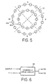
- FIG. 5 is a schematic plan view of the diffuse lighting rings 40a and 40b on the screen side.
- the LEDs are arranged in concentric rings, the inner ring being labelled I and the outer ring labelled O in the figure.
- the inner ring I is shown as consisting of 12 LEDs, and the outer ring O of 16 LEDs.
- the rings I, O are divided into quadrants in the xy plane as illustrated by the broken lines.
- the quadrants are labelled for convenience as north (N), south (S), east (E) and west (W).
- Opposing quadrants in each ring are tied together for control purposes, so that the diffuse screen lighting consists of four independently controllable light channels as follows:
- Each lighting channel can be switched on and off independently of the others, and also switched between the two current settings, by a respective drive circuit provided on the lighting control board 43.
- the drive circuit for one channel, channel A is illustrated schematically in Figure 6.
- the drive circuit 60 controls the two quadrants ON and OS together in response to two inputs from a controller on the board 43 to be described below.
- the drive circuit 60 receives an ENABLE input which can be either high or low depending on whether the channel A LEDs are to be on or off. By switching this ENABLE input between its two states, the light output can be pulsed.
- the circuit 60 also receives a high/low (H/L) input for switching between high and low intensity by varying the current through the channel A LEDs.
- H/L high/low
- a current of 550mA may be selected, and when the H/L input is low a current of 70mA may be selected.
- Suitable transistor logic for implementing the drive circuit will be readily apparent to those skilled in the art.
- Three similar drive circuits 60 are provided for the lighting channels B to D, each circuit receiving ENABLE and H/L inputs from the controller, and each controlling the associated pair of LED quadrants.
- one further drive circuit is provided on the control board 43 for controlling the direct screen LED 33, which therefore constitutes a further lighting channel, channel E.
- the channel E drive circuit operates similarly to the drive circuit 60, receiving ENABLE and H/L inputs, but in this case drives only the single LED 33.
- the high/low current settings for the direct LED 30 in this embodiment are different, namely 800mA and 100mA respectively.
- Figure 7 shows the main control circuitry on the lighting control board 43 for controlling the drive circuits for the five lighting channels A to E.
- the control circuitry comprises a microcontroller 62 which, as indicated, has five pairs of outputs connected to the ENABLE and H/L inputs of the drive circuits for the five lighting channels A to E.
- the controller 62 has a control input 64 which is used to set the lighting mode to one of three modes, namely off, continuous or triggered, and also to set the current level (high or low) and pulse width (ENABLE high period) for each of the lighting channels.
- the control signals are supplied to the control input 64 from the vision processor 8 and operator interface 9b ( Figure 1) in use.
- the controller 62 also has a trigger input 65 which, in the triggered mode of operation, receives trigger signals from the vision processor 8, for triggering the light pulses.
- the control circuitry also includes a sync separator 66 which receives the video signal from the CCD camera 21 for timing of the light pulses in the continuous mode of operation.
- the sync separator 66 extracts the vertical sync pulse from the video signal and supplies this to the controller 62, together with a field polarity signal O/E which indicates the polarity, ie. odd or even, of the video fields.
- the controller 62 also has an output 67 which is connected to the control input of a corresponding microcontroller on the lighting control board 44 for controlling lighting of the board 1.
- the board lighting control circuitry corresponds generally to the screen lighting control circuitry just described, having a microcontroller corresponding to the screen lighting controller 62, with corresponding inputs and outputs for controlling the equivalent lighting channels A to E on the board side via drive circuits as described above.
- the screen controller 62 acts as a master controller, relaying control signals, indicating operational mode and board lighting settings, received on its input 64 via the output 67 to the board controller.
- the board controller could receive its control inputs directly from the vision processor/operator interface.
- intensity adjustment is also provided by controlling the ENABLE inputs to vary the duration of light pulses emitted by each light channel. Specifically, by varying the ON time of a light channel, the width of the resulting light pulse can be varied to effectively provide further intensity adjustment.
- the pulse widths for each channel can be set by an operator from the operator interface 9b ( Figure 1) and input to the lighting control circuitry via the control input 64 of the controller 62 in Figure 7. The controller 62 then determines the start times for the pulses on each channel so that the pulse widths for all channels activated are centred on the same point in time.
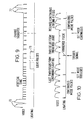
- FIG. 8 illustrates this for the lighting channels A to E of the screen lighting.
- channels A and C are set to the low current setting and a pulse width of 90 microseconds.
- Channels B and D are set to the high current setting with a pulse width of 30 microseconds.
- Channel E (the direct screen lighting) is set to the high current setting (which is greater than that for the diffuse lighting channels) with a pulse width of 20 microseconds.
- Figure 8 illustrates one example for the screen lighting only
- the controller 62 identifies the longest pulse width from the input settings, and computes the ENABLE switching times for the active channels accordingly.
- the switching information for the board lighting is relayed by the controller 62 to the board lighting control circuitry.
- the board controller could perform the necessary calculations independently.
- the lighting control circuitry is operable in continuous and triggered modes.
- the continuous mode of operation can be used for set-up purposes, to allow the operator to adjust and optimise the various settings.
- the continuous mode can also be used for inspection purposes, to allow the operator to check the screen, for example for aperture blockage or contamination, and to check the printed board for missing print, misaligned print, or excess print causing individual print features to join together.
- any combination of the screen and board lighting channels may be activated as required, though at least some of the diffuse lighting channels are usually used for inspection purposes. Whatever channels are activated, in the continuous mode each channel emits one pulse per frame of the video signal relayed to the vision processor, the pulses being centred on the same point in time as described above.
- the pulse timing is synchronised with the video signal in accordance with the Vsync and field polarity signals O/E derived by the sync separator 66 in Figure 7 and the corresponding sync separator of the board lighting control circuit. Specifically, the pulse timing is sequenced from the trailing edge of the vertical sync pulse in each odd field. This is illustrated in Figure 9 which shows an example of the timing of the light pulses relative to the video signal output by the CCD 21 which is of the interline transfer type in this case. In Figure 9, the line outputs from the previous field (even field) are indicated at 70. These are followed by the vertical sync signal which is detected by the sync separators to provide the Vsync output to the lighting controllers.
- the controllers then commence the light pulse sequencing for the active channels as indicated schematically at 71. This momentarily illuminates the screen and/or board, depending on the active channels, and the resulting image is captured by the CCD 21. Following the charge transfer operation in the CCD, the image data is readout in the following two fields of the video signal, the first few lines being indicated at 72.
- the triggered mode of operation light pulses from the active channels are again sequenced so as to be coincident in time as described above, but the channels are only activated periodically in response to a trigger signal supplied by the vision processor to the trigger inputs 65 of the screen and board controllers.
- This mode is used for fiducial capture, when the probe is moved automatically along a path through the fiducial locations, and at each location, acquires a simultaneous image of the screen and board fiducials. Only the board and screen direct lighting channels are generally used for the fiducial capture process. However, diffuse lighting channels can also be operated in the triggered mode if desired, eg. in an automated inspection process.
- Figure 10 illustrates the light pulse timing in relation to the output video signal over a transition between continuous and triggered modes.
- a wide range of lighting conditions can be achieved by selecting the current setting, and varying the pulse width, for each light channel independently.
- the pulse width should preferably be short in comparison with the video field period, but can still be adjusted over a wide range, for example between 10 and 250 microseconds. It will be appreciated that, in the continuous mode, a pseudo-continuous lighting effect is achieved allowing continuous monitoring by an operator while the probe is in motion without problems of image blur and while still providing the same lighting effects as in the triggered mode. Moreover, since the pulses are synchronised with the video signal, image flicker is avoided. Further, in both continuous and triggered modes, though the pulse width varies between light channels, the pulses are centred on the same point in time to ensure that the moving image is effectively frozen in the same position by each light channel.
Landscapes
- Physics & Mathematics (AREA)
- General Physics & Mathematics (AREA)
- Investigating Materials By The Use Of Optical Means Adapted For Particular Applications (AREA)
- Closed-Circuit Television Systems (AREA)
- Studio Devices (AREA)
Description
Claims (7)
- Imaging apparatus for acquiring images of regions, in particular of a screen (2) and/or board (1) in a screen printer, the apparatus comprising:characterized in that:a plurality of lighting means for illuminating regions to be imaged; andimaging means (8, 21) for acquiring images of the regions illuminated by the lighting means;the apparatus further comprises control means (43, 44, 60, 62) for controlling each lighting means to generate a pulse of light, wherein the control means (43, 44, 60, 62) is operable to control the plurality of lighting means to generate respective pulses of different durations such that the temporal midpoints of pulses from respective lighting means are coincident.
- Apparatus as claimed in claim 1, wherein the control means (43, 44, 60, 62) is operable to vary the pulse duration of one or more of the lighting means in response to a control signal (64).
- Apparatus as claimed in claim 1 or 2, wherein the plurality of lighting means comprises direct lighting means (32) for illuminating the regions with substantially collimated light.
- Apparatus as claimed in any of claims I to 3, wherein the plurality of lighting means comprises diffuse lighting means (40a, 40b, 41a, 41b) for illuminating the regions with diffuse light.
- Apparatus as claimed in any of claims 1 to 4, wherein the control means (43, 44, 60, 62) is operable to control the plurality of lighting means to generate respective pulses repeatedly.
- Apparatus as claimed in any of claims 1 to 5, wherein the control means (43, 44, 60, 62) is operable to control the plurality of lighting means to generate respective pulses of light in response to an external control signal (65) received by the control means (43, 44, 60, 62).
- A method of acquiring images of regions, in particular of a screen (2) and/or board (1) in a screen printer, the method comprising the steps of:characterized in that:illuminating regions to be imaged by a plurality of lighting means; andacquiring images of the regions illuminated by the lighting means;the step of illuminating regions to be imaged comprises the step of operating a plurality of lighting means to generate respective pulses of light for illuminating the regions to be imaged; andthe method further comprises the step of controlling the plurality of lighting means to generate respective pulses of different durations such that the temporal midpoints of pulses from respective lighting means are coincident.
Applications Claiming Priority (3)
| Application Number | Priority Date | Filing Date | Title |
|---|---|---|---|
| GB9706148 | 1997-03-25 | ||
| GB9706148A GB2323664A (en) | 1997-03-25 | 1997-03-25 | Viewing and imaging systems |
| PCT/GB1998/000696 WO1998042510A2 (en) | 1997-03-25 | 1998-03-09 | Viewing and imaging systems |
Publications (2)
| Publication Number | Publication Date |
|---|---|
| EP1011973A2 EP1011973A2 (en) | 2000-06-28 |
| EP1011973B1 true EP1011973B1 (en) | 2003-07-02 |
Family
ID=10809814
Family Applications (1)
| Application Number | Title | Priority Date | Filing Date |
|---|---|---|---|
| EP98910851A Expired - Lifetime EP1011973B1 (en) | 1997-03-25 | 1998-03-09 | Viewing and imaging systems |
Country Status (5)
| Country | Link |
|---|---|
| US (1) | US6621517B1 (en) |
| EP (1) | EP1011973B1 (en) |
| DE (1) | DE69816098T2 (en) |
| GB (1) | GB2323664A (en) |
| WO (1) | WO1998042510A2 (en) |
Families Citing this family (23)
| Publication number | Priority date | Publication date | Assignee | Title |
|---|---|---|---|---|
| JP2000238233A (en) | 1999-02-23 | 2000-09-05 | Fuji Mach Mfg Co Ltd | Method and equipment for inspecting screen, and screen printer |
| JP3704271B2 (en) * | 2000-04-10 | 2005-10-12 | 三菱電機株式会社 | IMAGING DEVICE AND CELL PHONE HAVING THE SAME |
| JP2001293842A (en) * | 2000-04-14 | 2001-10-23 | Minami Kk | Screen printing device |
| WO2003098920A1 (en) * | 2002-05-16 | 2003-11-27 | Koninklijke Philips Electronics N.V. | Image sensor device |
| GB2403003B (en) * | 2003-06-19 | 2006-06-07 | Dek Int Gmbh | Inspection system for and method of inspecting deposits printed on workpieces |
| DE102005043833A1 (en) * | 2005-09-13 | 2007-03-29 | Ersa Gmbh | Device for determining the relative position between two substantially flat elements |
| US20070102478A1 (en) * | 2005-11-10 | 2007-05-10 | Speedline Technologies, Inc. | Optimal imaging system and method for a stencil printer |
| US20070102477A1 (en) * | 2005-11-10 | 2007-05-10 | Speedline Technologies, Inc. | Imaging system and method for a stencil printer |
| JP4696861B2 (en) * | 2005-11-11 | 2011-06-08 | パナソニック株式会社 | Screen printing device |
| US7458318B2 (en) * | 2006-02-01 | 2008-12-02 | Speedline Technologies, Inc. | Off-axis illumination assembly and method |
| US7549371B2 (en) * | 2006-07-10 | 2009-06-23 | Speedline Technologies, Inc. | Method and apparatus for clamping a substrate |
| US7710611B2 (en) * | 2007-02-16 | 2010-05-04 | Illinois Tool Works, Inc. | Single and multi-spectral illumination system and method |
| US7861650B2 (en) * | 2007-04-13 | 2011-01-04 | Illinois Tool Works, Inc. | Method and apparatus for adjusting a substrate support |
| DE102007019073A1 (en) * | 2007-04-23 | 2008-11-06 | Ekra Automatisierungssysteme Gmbh Asys Group | Method and device for applying media to flat substrates |
| US8215473B2 (en) * | 2008-05-21 | 2012-07-10 | Applied Materials, Inc. | Next generation screen printing system |
| JP5409120B2 (en) * | 2009-05-27 | 2014-02-05 | キヤノン株式会社 | Correction method, apparatus, and device manufacturing method |
| US20140098216A1 (en) * | 2012-10-08 | 2014-04-10 | Dwfritz Automation Inc. | Simultaneous-view object insertion systems, apparatuses and methods |
| EP3776079B1 (en) | 2018-04-06 | 2023-06-07 | Esko-Graphics Imaging GmbH | Method for persistent marking of flexo plates with workflow information and plates marked therewith |
| US11724533B2 (en) | 2018-04-06 | 2023-08-15 | Esko-Graphics Imaging Gmbh | System and process for persistent marking of flexo plates and plates marked therewith |
| US10883704B2 (en) * | 2019-03-29 | 2021-01-05 | Robe Lighting S.R.O. | Homogenization system for an LED luminaire |
| EP4042245B1 (en) | 2019-10-07 | 2023-09-27 | Esko-Graphics Imaging GmbH | System and process for persistent marking of flexo plates and plates marked therewith |
| EP4174579B1 (en) * | 2021-11-01 | 2025-07-02 | Esko-Graphics Imaging GmbH | System and process for persistent marking of flexo plates with isolated microstructures and plates marked therewith |
| EP4589386A3 (en) * | 2021-11-01 | 2025-10-01 | Esko-Graphics Imaging GmbH | System and process for persistent marking of flexo plates with isolated microstructures and plates marked therewith |
Citations (1)
| Publication number | Priority date | Publication date | Assignee | Title |
|---|---|---|---|---|
| US4385238A (en) * | 1981-03-03 | 1983-05-24 | Veeco Instruments Incorporated | Reregistration system for a charged particle beam exposure system |
Family Cites Families (12)
| Publication number | Priority date | Publication date | Assignee | Title |
|---|---|---|---|---|
| US4253447A (en) * | 1978-10-16 | 1981-03-03 | Welch Allyn, Inc. | Color endoscope with charge coupled device and television viewing |
| JPS5972728A (en) * | 1982-10-20 | 1984-04-24 | Canon Inc | Automatic alignment device |
| IT1184602B (en) | 1985-06-10 | 1987-10-28 | Ezio Curti | PROCEDURE AND MEANS FOR PRINTING THE PATH OF AN ELECTRONIC CIRCUIT IN THE REGISTER COMPARED TO HOLES PRACTICED IN A SUPPORT PLATE |
| US4651203A (en) | 1985-10-29 | 1987-03-17 | At&T Technologies, Inc. | Video controlled article positioning system |
| GB2212689B (en) * | 1987-11-17 | 1992-01-02 | Ferranti Plc | Television camera system |
| DE3928527A1 (en) | 1989-08-29 | 1991-03-14 | Ind Siebdruck Systeme Neckarwe | Flat bed screen printing machine for PCB(s) - has two cameras with endoscopes slidable between PCB in load position and screen |
| US5060063A (en) * | 1990-07-30 | 1991-10-22 | Mpm Corporation | Viewing and illuminating video probe with viewing means for simultaneously viewing object and device images along viewing axis and translating them along optical axis |
| JPH0596700A (en) | 1991-10-04 | 1993-04-20 | Murata Mfg Co Ltd | Method for registration in screen printing |
| DE4217430A1 (en) | 1992-05-27 | 1993-12-02 | Autronic Bildverarbeitung | Pick=up arrangement for detecting and representing objects for comparison - has electronic camera and prismatic deflection devices forming partial images of simultaneously detected object regions |
| US5257063A (en) * | 1992-09-30 | 1993-10-26 | Olympus Optical Co., Ltd. | Flashing controller |
| GB9323978D0 (en) | 1993-11-22 | 1994-01-12 | Dek Printing Machines Ltd | Alignment systems |
| US5943089A (en) | 1996-08-23 | 1999-08-24 | Speedline Technologies, Inc. | Method and apparatus for viewing an object and for viewing a device that acts upon the object |
-
1997
- 1997-03-25 GB GB9706148A patent/GB2323664A/en not_active Withdrawn
-
1998
- 1998-03-09 EP EP98910851A patent/EP1011973B1/en not_active Expired - Lifetime
- 1998-03-09 WO PCT/GB1998/000696 patent/WO1998042510A2/en not_active Ceased
- 1998-03-09 DE DE69816098T patent/DE69816098T2/en not_active Expired - Lifetime
- 1998-03-09 US US09/380,950 patent/US6621517B1/en not_active Expired - Lifetime
Patent Citations (1)
| Publication number | Priority date | Publication date | Assignee | Title |
|---|---|---|---|---|
| US4385238A (en) * | 1981-03-03 | 1983-05-24 | Veeco Instruments Incorporated | Reregistration system for a charged particle beam exposure system |
Also Published As
| Publication number | Publication date |
|---|---|
| US6621517B1 (en) | 2003-09-16 |
| WO1998042510A2 (en) | 1998-10-01 |
| GB9706148D0 (en) | 1997-05-14 |
| GB2323664A (en) | 1998-09-30 |
| DE69816098D1 (en) | 2003-08-07 |
| DE69816098T2 (en) | 2004-04-15 |
| WO1998042510A3 (en) | 1998-11-05 |
| EP1011973A2 (en) | 2000-06-28 |
Similar Documents
| Publication | Publication Date | Title |
|---|---|---|
| US6621517B1 (en) | Viewing and imaging systems | |
| KR100497636B1 (en) | Electronic component mounting apparatus | |
| US5752446A (en) | Alignment systems | |
| EP0385625B1 (en) | Method and apparatus for inspection of substrates | |
| US20070102477A1 (en) | Imaging system and method for a stencil printer | |
| CN104024835A (en) | Automatic visual inspection device | |
| US20070102478A1 (en) | Optimal imaging system and method for a stencil printer | |
| JP3955206B2 (en) | Component mounting method and component mounting apparatus | |
| JP2000124683A (en) | Image pickup of electronic component and electronic component mounting equipment | |
| US7019771B1 (en) | Inspection device for components | |
| JP4315752B2 (en) | Electronic component mounting equipment | |
| US20050157920A1 (en) | Machine vision system and method | |
| JP2001330619A (en) | Dispensing machine | |
| JP2000277999A5 (en) | ||
| KR101157158B1 (en) | Chip Recognition Apparatus for Chip-Mounter | |
| JP2008160136A (en) | Electronic component imaging method and electronic component mounting apparatus | |
| JP4123447B2 (en) | Electronic component imaging method and electronic component mounting apparatus | |
| KR100268251B1 (en) | Lighting brightness controller and component control method of component mounting machine | |
| JP3114347B2 (en) | One-dimensional CCD imaging device | |
| JPH11272838A5 (en) | ||
| JP2005236323A (en) | Electronic component mounting method and electronic component mounting apparatus | |
| HK1010706B (en) | Alignment systems | |
| KR20030011175A (en) | Soldering inspection apparatus | |
| JPH06109651A (en) | Defect inspection equipment |
Legal Events
| Date | Code | Title | Description |
|---|---|---|---|
| PUAI | Public reference made under article 153(3) epc to a published international application that has entered the european phase |
Free format text: ORIGINAL CODE: 0009012 |
|
| 17P | Request for examination filed |
Effective date: 19990908 |
|
| AK | Designated contracting states |
Kind code of ref document: A2 Designated state(s): DE FR GB |
|
| 17Q | First examination report despatched |
Effective date: 20010319 |
|
| GRAH | Despatch of communication of intention to grant a patent |
Free format text: ORIGINAL CODE: EPIDOS IGRA |
|
| RAP1 | Party data changed (applicant data changed or rights of an application transferred) |
Owner name: DEK INTERNATIONAL GMBH |
|
| GRAH | Despatch of communication of intention to grant a patent |
Free format text: ORIGINAL CODE: EPIDOS IGRA |
|
| GRAA | (expected) grant |
Free format text: ORIGINAL CODE: 0009210 |
|
| AK | Designated contracting states |
Designated state(s): DE FR GB |
|
| REG | Reference to a national code |
Ref country code: GB Ref legal event code: FG4D |
|
| REF | Corresponds to: |
Ref document number: 69816098 Country of ref document: DE Date of ref document: 20030807 Kind code of ref document: P |
|
| ET | Fr: translation filed | ||
| PLBE | No opposition filed within time limit |
Free format text: ORIGINAL CODE: 0009261 |
|
| STAA | Information on the status of an ep patent application or granted ep patent |
Free format text: STATUS: NO OPPOSITION FILED WITHIN TIME LIMIT |
|
| 26N | No opposition filed |
Effective date: 20040405 |
|
| REG | Reference to a national code |
Ref country code: DE Ref legal event code: R082 Ref document number: 69816098 Country of ref document: DE Representative=s name: WSL PATENTANWAELTE PARTNERSCHAFTSGESELLSCHAFT, DE |
|
| REG | Reference to a national code |
Ref country code: DE Ref legal event code: R082 Ref document number: 69816098 Country of ref document: DE Representative=s name: WSL PATENTANWAELTE PARTNERSCHAFT MBB, DE Effective date: 20130702 Ref country code: DE Ref legal event code: R082 Ref document number: 69816098 Country of ref document: DE Representative=s name: WSL PATENTANWAELTE PARTNERSCHAFTSGESELLSCHAFT, DE Effective date: 20130702 Ref country code: DE Ref legal event code: R081 Ref document number: 69816098 Country of ref document: DE Owner name: ASM ASSEMBLY SYSTEMS SINGAPORE PTE LTD., SG Free format text: FORMER OWNER: DEK INTERNATIONAL GMBH, ZUERICH, CH Effective date: 20130702 Ref country code: DE Ref legal event code: R081 Ref document number: 69816098 Country of ref document: DE Owner name: DTG INTERNATIONAL GMBH, CH Free format text: FORMER OWNER: DEK INTERNATIONAL GMBH, ZUERICH, CH Effective date: 20130702 |
|
| REG | Reference to a national code |
Ref country code: FR Ref legal event code: CD Owner name: DTG INTERNATIONAL GMBH, CH Effective date: 20130904 Ref country code: FR Ref legal event code: CA Effective date: 20130904 |
|
| REG | Reference to a national code |
Ref country code: FR Ref legal event code: PLFP Year of fee payment: 19 |
|
| REG | Reference to a national code |
Ref country code: FR Ref legal event code: PLFP Year of fee payment: 20 |
|
| PGFP | Annual fee paid to national office [announced via postgrant information from national office to epo] |
Ref country code: DE Payment date: 20170322 Year of fee payment: 20 Ref country code: FR Payment date: 20170322 Year of fee payment: 20 |
|
| PGFP | Annual fee paid to national office [announced via postgrant information from national office to epo] |
Ref country code: GB Payment date: 20170322 Year of fee payment: 20 |
|
| REG | Reference to a national code |
Ref country code: DE Ref legal event code: R082 Ref document number: 69816098 Country of ref document: DE Representative=s name: WSL PATENTANWAELTE PARTNERSCHAFT MBB, DE Ref country code: DE Ref legal event code: R081 Ref document number: 69816098 Country of ref document: DE Owner name: ASM ASSEMBLY SYSTEMS SINGAPORE PTE LTD., SG Free format text: FORMER OWNER: DTG INTERNATIONAL GMBH, ZUERICH, CH |
|
| REG | Reference to a national code |
Ref country code: GB Ref legal event code: 732E Free format text: REGISTERED BETWEEN 20170817 AND 20170823 |
|
| REG | Reference to a national code |
Ref country code: FR Ref legal event code: CD Owner name: ASM ASSEMBLY SYSTEMS SINGAPORE PTE. LTD., SG Effective date: 20171122 |
|
| REG | Reference to a national code |
Ref country code: FR Ref legal event code: TP Owner name: ASM ASSEMBLY SYSTEMS SINGAPORE PTE. LTD., SG Effective date: 20171127 |
|
| REG | Reference to a national code |
Ref country code: DE Ref legal event code: R071 Ref document number: 69816098 Country of ref document: DE |
|
| REG | Reference to a national code |
Ref country code: GB Ref legal event code: PE20 Expiry date: 20180308 |
|
| PG25 | Lapsed in a contracting state [announced via postgrant information from national office to epo] |
Ref country code: GB Free format text: LAPSE BECAUSE OF EXPIRATION OF PROTECTION Effective date: 20180308 |