EP1011217A2 - Optischer Zwischenverstärker - Google Patents
Optischer Zwischenverstärker Download PDFInfo
- Publication number
- EP1011217A2 EP1011217A2 EP99124869A EP99124869A EP1011217A2 EP 1011217 A2 EP1011217 A2 EP 1011217A2 EP 99124869 A EP99124869 A EP 99124869A EP 99124869 A EP99124869 A EP 99124869A EP 1011217 A2 EP1011217 A2 EP 1011217A2
- Authority
- EP
- European Patent Office
- Prior art keywords
- optical
- electrical
- wavelength
- signal
- output
- Prior art date
- Legal status (The legal status is an assumption and is not a legal conclusion. Google has not performed a legal analysis and makes no representation as to the accuracy of the status listed.)
- Withdrawn
Links
Images


Classifications
-
- H—ELECTRICITY
- H04—ELECTRIC COMMUNICATION TECHNIQUE
- H04B—TRANSMISSION
- H04B10/00—Transmission systems employing electromagnetic waves other than radio-waves, e.g. infrared, visible or ultraviolet light, or employing corpuscular radiation, e.g. quantum communication
- H04B10/29—Repeaters
Definitions
- the present invention relates to a repeater for reproducing and relaying the signal of which optical signal waveform is deteriorated in the optical transmission line in the optical communication system utilizing optical beam such as optical transmission system, optical add-drop system and optical cross-connection system and an optical repeater for converting optical wavelength to be transmitted by the optical communication system to different optical wavelength in the course of transmission in order to form a flexible system which can process the optical signals of different bit rates and different pulse duty.
- optical beam such as optical transmission system, optical add-drop system and optical cross-connection system
- an optical repeater for converting optical wavelength to be transmitted by the optical communication system to different optical wavelength in the course of transmission in order to form a flexible system which can process the optical signals of different bit rates and different pulse duty.
- optical devices such as optical fiber, optical amplifier, branching filter for wavelength multiplexing, optical add-drop multiplexer and optical switch or the like basically does not depend on the bit rate and pulse duty, etc. of the signal to be transmitted but such bit rate and duty are generally fixed for the optical repeater for reproducing waveform accompanied by optical-electrical conversion and optical wavelength converter accompanied by optical-electrical conversion.
- FIG. 13 illustrates an example of a reproducing type optical repeater of the related art.
- the existing reproducing type optical repeater optical-electrically converts an input optical signal with a optical-electrical converting means (1).
- the signal converted to an electrical signal by the optical-electrical converting means (1) is then amplified by an amplifier (2).
- An output of the amplifier (1) extracts the clock from an electrical signal with a timing extracting circuit (79).
- the signal waveform dulled by transmission can be reproduced by identifying the electrical signal from the amplifier (2) in the discriminating circuit (6) with the clock.
- the bit rate to be processed for timing reproduction by the timing extracting circuit depends on the timing extracting circuit and the bit rate is fixed by the timing extracting circuit structure and the pulse duty to be processed can also be fixed.
- This repeater is a reproducing type repeater designed for processing a plurality of bit rates.
- bit rate detecting means a PLL, a frequency dividing circuit and a switch are comprised to process the maximum frequency and the maximum frequency of bit rate of 1/2 exponent.
- the bit rate to be processed depends on the timing extracting circuit and the bit rate is fixed by the timing extracting circuit structure because the timing is reproduced by the timing extracting circuit.
- the pulse duty to be processed can also be fixed.
- bit rates can be processed but is limited to the particular bit rate and the signals of other bit rates and different pulse duty cannot be processed.
- a current wavelength converting apparatus converts an optical signal to an electrical signal using an ordinary optical repeater and transmits an optical signal using a new light source.
- This structure also has a program which is the same problem of the optical repeater of the related art.
- the present invention realizes an optical repeater which assures free use of bit rate and duty of an input signal by adjusting, after conversion of optical signal into an electrical signal, the waveform and duty and then converting this signal by the electrical-optical conversion.
- the present invention realizes bit rate free wavelength conversion by changing wavelength of the optical signal output from an optical repeater in regard to the wavelength of optical signal to be input to the optical repeater.
- the electrical-optical converting means should be designed as the circuit structure corresponding to the maximum transmission rate used in the transmission line and is provided as the individual unit different from the other circuits.
- repeaters may be used for optical wavelength terminal, optical branching/inserting apparatus and optical cross-connection apparatus.
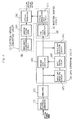
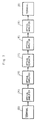
- Fig. 1 is a diagram illustrating a structure of the present invention.
- 1 designates an optical-electrical converter; 2, an amplifier; 3, a waveform shaping circuit; 4, a duty reproducing circuit and 5, an electrical-optical converting circuit.
- the optical-electrical converter 1 converts an optical signal into an electrical signal.
- the amplifier 2 amplifies an electrical signal from the optical-electrical converter 1.
- the waveform shaping circuit 3 improves deterioration of waveform generated by noise in the high level and low level sides of the binary digital signal as the electrical signal from the amplifier 2, transmission through fiber (wavelength dispersion, non-linear effect, polarized dispersion) and imperfect circuit design.
- the duty reproducing circuit 4 recovers the pulse duty changed by the fiber transmission and waveform reproducing means 3 to the duty before the change.
- the electrical-optical converting circuit 5 converts an electrical signal to an optical signal by electrical-optical conversion with an electrical signal of which duty is recovered by the duty reproducing circuit 4.
- the waveform conversion can also be realized by changing wavelength with the electrical-optical converting circuit 5 to the wavelength different from the optical wavelength input in the optical-electrical converter 1.
- the present invention can form the pulse waveform without reproducing of retiming by adjusting the duty through waveform shaping and does not accumulate changes of pulse duty due to the fiber transmission of the high speed signal.
- waveform formation transmission quality improvement
- waveform conversion are possible for the optical signal of the freely selected bit rate and pulse duty less than the maximum operation bit rate determined by the circuit characteristic without any restriction on the bit rate and pulse duty.
- the optical signal of amplitude modulation input to the optical-electrical converter 1 can be output through conversion of modulation system to the optical phase modulation or optical frequency modulation depending on the selection of the means for modulating the light beam in the electrical-optical converting circuit.
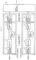
- Fig. 2 is a first practical example of the structure of Fig. 1.
- the optical-electrical converter 1 converts the optical amplitude modulated digital signal in which waveform deterioration is generated through transmission by the transmission line to an electrical signal.
- This optical-electrical converter 1 is structured by a light receiving element such as PIN photo-diode and an avalanche diode.
- the amplifier 2 amplifies an electrical signal from the optical-electrical converter 1.
- the waveform shaping circuit 3 is formed of a slice amplifier.
- the first slice amplifier 31of the waveform shaping circuit 3 improves waveform distortion and waveform dull generated by noise, fiber transmission and imperfect circuit design to be included in the transmitted signal by cutting at the predetermined value the high level and low level sides of the electrical signal waveform amplified by the amplifier 2.
- the reference level of the first slice amplifier 31 of the waveform shaping circuit 3 it is preferable to set the reference level of the first slice amplifier 31 of the waveform shaping circuit 3 to the optimum level from the viewpoint of SN ratio.
- the duty reproducing circuit 4 is composed of second slice amplifier 41, input duty detector 42, duty control circuit 43 and output duty detector 44. [0046]
- the input duty detector 42 determines whether the duty of optical signal is 50% or 100%.
- the second slice amplifier 41 recovers the pulse duty to that before the change caused by the optical transmission and first slice amplifier 31 by cutting an output of the first slice amplifier 31 at the reference level from the duty control circuit 43.
- the output duty detector 44 detects the output duty of the second slice amplifier 41 and then notifies the detection result to the duty control circuit 43. [0049]
- the duty control circuit 43 controls the reference level of the second slice amplifier 41 based on the result of the input duty detector 42 and output duty detector 44.
- the electrical-optical converting circuit 5 is composed of optical modulation drive circuit 51, semiconductor laser 52, optical modulator 54 and wavelength stabilizing circuit 53. [0051]
- the optical modulation drive circuit 51 drives the optical modulator 54 with an output from the second slice amplifier 41.
- the optical modulator 54 is formed of an external modulator such as the Mach-Zehnder type optical modulator and electrolytic absorption type semiconductor modulator or the like which realizes amplitude modulation by forming an optical waveguide on the lithium niobate substrate and giving phase difference to the light beam with an electrode formed on the optical waveguide.
- an external modulator such as the Mach-Zehnder type optical modulator and electrolytic absorption type semiconductor modulator or the like which realizes amplitude modulation by forming an optical waveguide on the lithium niobate substrate and giving phase difference to the light beam with an electrode formed on the optical waveguide.
- This optical modulator 54 executes the optical-amplitude modulation to the light beam from the semiconductor laser 52 with the signal from the optical modulation drive circuit 51 to provide an optical output signal.
- Amplitude modulation is basically preferable as the modulation system for the optical output of the optical modulator but the optical-phase modulation and optical-frequency modulation are also possible by changing combination of the output format of the optical modulation drive circuit 51 and optical modulator 54. [0055]
- the waveform stabilizing circuit 53 stabilizes optical wavelength by monitoring a rear side output of the semiconductor laser 52 to stabilize an output of the semiconductor laser 52 to the light beam of constant wavelength and controlling both or any one of temperature and drive current.
- Fig. 3 is a second practical example of the structure of Fig. 1.
- FIG. 3 Structure of Fig. 3 is an example where the direct modulation is performed by the semiconductor laser 52 in the structure of the electrical-optical converting circuit 5 having the structure of Fig. 1. Other structures and operations are similar to those of Fig. 2. [0059]
- the electrical-optical converting circuit 5 varies a bias current of semiconductor laser 52 in the modulation drive circuit 51 with an output from the duty reproducing circuit 4 and changes an optical output level of the semiconductor laser 52 for optical amplitude modulation.
- Fig. 4 illustrates a third practical example of the structure of Fig. 1.
- the input duty detector 42 outputs the result of determination to the duty control circuit 43 by deciding the duty of an electrical signal amplified by the amplifier 2 to 50% or 100%.
- the output duty detector 44 detects the output duty of the second slice amplifier 42 and outputs the detection result to the duty control circuit 43.
- the duty control circuit 43 adjusts duty by controlling the reference level of the second slice amplifier 41 with an output of the input duty detector 42 and an output of the output duty detector 44.
- the second slice amplifier 41 changes duty of electrical signal by cutting an electrical signal output from the amplifier at the predetermined reference level under the reference level control by the duty control circuit 43.
- the first slice amplifier 31 is capable of reproducing the pulse waveform, in order to form waveform of an output of the second slice amplifier 41, by amplifying an output of the second slice amplifier 41 and cutting the peak value and bottom value at the predetermined levels. Since the waveform shaping circuit 3 is located after the duty reproducing circuit , duty changes a little but such change of duty can be minimized by providing the structure which results in higher amplifier gain. [0069]
- the structure of electrical-optical converting circuit 5 may be replaced with the structure of optical-electrical converting circuit 5.
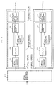
- Fig. 5 illustrates a practical structure of the duty reproducing circuit illustrated in Fig. 2 to Fig. 4.
- the input duty detector 42 is structured by average value detecting circuit 421, peak value detecting circuit 422 and duty deciding circuit 423. [0072]
- the first slice amplifier 31 inputs an output of the amplifier 2 to an average value detecting circuit 421 and a peak value detecting circuit 422.
- the average value detecting circuit 421 detects the average value of the signal waveform and then inputs it to the duty deciding circuit 423.
- the peak value detecting circuit 422 detects the peak value of the signal waveform and inputs it to the duty deciding circuit 423.
- the duty deciding circuit 423 detects a ratio of the peak value and average value based on the outputs of average value detecting circuit 421 and peak value detecting circuit 422 in order to decide that the pulse duty of input electrical signal is 50% or 100% and then outputs the result to the duty control circuit.
- the pulse duty of an input electrical signal is decided to be 50% or 100% because the transmission code used in general by optical communication is RZ signal (duty: 50%) or NRZ signal(duty: 100%).
- the duty deciding means 423 not only decides that the duty is 50% or 100% as explained above but also can be used in the system in which particular duty is used for the encoding system of transmission system. [0078]
- duty can be set freely depending on the input signal by outputting, to the duty detecting circuit, the analog result detected on the basis of outputs of the average value detecting circuit 421 and peak value detecting circuit 422.
- An output duty detector 44 is composed of an average value detecting circuit 441, a peak value detecting circuit 442 and a duty detecting circuit 443.
- An output of the second slice amplifier 41 is input to both the average value detecting circuit 441 and peak value detecting circuit 442.
- the average value detecting circuit 441 detects the average value of signal waveform and then inputs it to a duty deciding circuit 443. [0082]
- the peak value detecting circuit 442 detects the peak value of signal waveform and inputs it to the duty deciding circuit 423.
- the duty detecting circuit 443 obtains a ratio of the outputs of the average value detecting circuit 441 and peak value detecting circuit 442 to detect a duty ratio of the output of the second slice amplifier 41 and then outputs this result to the duty control circuit 43.
- the duty control circuit 43 controls the reference level of the second slice amplifier based on the result of the duty deciding circuit 423 and duty detecting circuit 443.
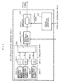
- Fig. 6 illustrates a structure of the electrical-optical converting circuit 5 in the optical repeater for waveform conversion.
- 55 designates a laser bank composed of semiconductor lasers 553-1 to 553-n, waveform stabilizing circuits 554-1 to 554-n and a waveform combiner 552.
- the semiconductor lasers 553-1 to 553-n are controlled in the temperature and drive current by the waveform stabilizing circuits 554-1 to 554-n to provide different waveform outputs.
- Optical outputs of the semiconductor lasers 553-1 to 553-n are waveform- multiplexed by the waveform combiner 552.
- the light beam of the particular waveform among the waveform-multiplexed optical signal is selected by an optical waveform selecting filter 551 and is then output to the optical modulator 52.
- This optical waveform selecting filter 551 is formed using a filter which can freely vary the pass-band frequency of an acoustic optic tunable filter (AOTF), etc. with an external signal.
- AOTF acoustic optic tunable filter
- Instruction for waveform selection can be issued from an apparatus outside the repeater or with a control signal for selected waveform switching of AOFT by reproducing the monitor control signal included in the transmission signal.
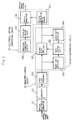
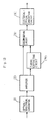
- Fig. 7 illustrates a structure of optical amplifying and repeating transmission system utilizing an optical repeater 7 of the structure illustrated in Fig. 1 to Fig. 7.
- the optical amplifying and repeating transmission system inputs an optical output from the terminal 8 to the optical repeater 7 via a plurality of optical amplifiers 9 (rare element doped optical fiber amplifier) for amplifying in direct the optical signal in the transmission line consisting of optical fiber.
- optical amplifiers 9 ultraviolet element doped optical fiber amplifier
- the optical repeater 7 converts the optical signal into an electrical signal with the structure illustrated in Fig. 1 to Fig. 6 and executes waveform shaping and also adjusts duty to convert the electrical signal to an optical signal for providing an output signal.
- This optical output in the transmission line consisting of optical fiber is then sent to the terminal 8 via a plurality of optical amplifiers 9 for amplifying in direct the optical signal.
- a repeater of the present invention When a repeater of the present invention is provided in the transmission line, a system for improving accumulated noise during relaying by optical amplifier and waveform deterioration due to fiber transmission for the long distance transmission can be formed not depending on the bit rate.
- Fig. 8 illustrates an example of structure of the waveform multiplex system utilizing optical repeater of Fig. 1 to Fig. 6 of the present invention.
- the optical signal is output through wavelength conversion to the predetermined wavelength, waveform shaping and duty reproduction by the optical repeater 7 of the structure of Fig. 1 to Fig. 6 of the present invention.
- This wavelength multiplexed optical signal is input to the wavelength multiplex repeater 102 via a plurality of optical amplifiers 9 for direct amplification of optical signal provided in the optical fiber.
- the wavelength multiplex repeater 702 branches the input optical wavelength multiplex signal corresponding to each wavelength by the wavelength demultiplexer 11, input these branching signals to the optical repeater 7 of the structure of Fig. 1 to Fig. 6 corresponding to each wavelength and then outputs these optical signals to the wavelength multiplexer 10 through waveform shaping and duty reproduction.
- the wavelength multiplexing mans 10 wavelength-multiplexes an output of each optical repeater 7 to output to the optical fiber transmission line.
- An output of the wavelength multiplexer 10 is input to the wavelength multiplex terminal 103 in the receiving side via a plurality of optical amplifiers 9 for direct amplification of optical signal provided in the optical fiber transmission line.
- the wavelength multiplex terminal 103 in the receiving side inputs the optical signals branched into respective wavelengths by the wavelength demultiplexer 11 to the optical repeater 7 of the structure of Fig. 1 to Fig. 6. [0103]
- Each repeater outputs the optical signal to each receiving terminal 8 through waveform shaping, duty reproducing, wavelength conversion to the predetermined wavelength.
- optical repeater of Fig. 1 to Fig. 6 of the present invention can be realized by applying, as explained above, the optical repeater of Fig. 1 to Fig. 6 of the present invention to the transponder (wavelength converting means) and repeater of the transmitting/receiving means.
- Fig. 9 illustrates an example of the optical add-drop system utilizing the optical repeaters 71-1 to 71-n of the structure of Fig. 1 to Fig. 6.
- the optical signal drop mans branches the optical signal transmitted through optical wavelength multiplexing to the optical signal of the particular wavelength and then outputs the signal to a tributary means 123 in the receiving side.
- the optical signal drop circuit branches the optical signal of particular wavelength through combination of the wavelength selection filter, fiber grating filter and circulator and then outputs the optical signal to the tributary means 124 in the receiving side.
- the tributary means 124 in the receiving side is composed of optical repeaters 71-1 to 71-n of the structure of Fig. 1 to Fig. 6 of the present invention and the terminals 81-1 to 81-n and can receives the signal with the terminals 81-1 to 81-n through waveform shaping, duty reproduction and wavelength conversion, if necessary, for each wavelength dropped by the optical signal drop circuit .
- optical signal not dropped to the tributary means in the receiving side by the optical signal drop circuit 121 is waveform-multiplexed with the optical signal from the tributary means 125 in the transmitting side and is then output as the optical signal output.
- the tributary means 125 in the transmitting side is composed of the terminals 82-1 to 82-n and the optical repeaters 72-1 to 72-n of the structure of Fig. 6. [0110]
- the optical repeaters 72-1 to 72-n execute the wavelength conversion for the optical outputs from the terminals 82-1 to 82-n to the optical signal add circuit 122 through waveform shaping, duty reproducing and wavelength conversion, if necessary.
- a common laser bank 55 is provided in place of common use in unit of optical repeater as illustrated in Fig. 6 and an output thereof is wavelength- selected by the wavelength selecting filter provided in each optical repeater and is then modulated by the optical modulator.
- the flexible add-drop of the optical signal in various bit rates and different pulse duties can be realized by applying the optical repeater of the structure of Fig. 1 to Fig. 6 of the present invention to the wavelength converting means of the tributary means.
- Fig. 10 illustrates a structure of the optical cross-connection system using the optical repeater of Fig. 1 to Fig. 6 of the present invention.
- a plurality of optical inputs are multiplexed into a plurality of optical signals by the branching filters 13-1 to 13-3 and are then input to optical matrix switch 200.
- optical signals changed in direction through the switching by the optical matrix switch 200 are then subjected to the waveform shaping and duty reproducing in the optical repeaters 7-1 to 7-n of the structure of Fig. 1 to Fig. 6, combined by the combiners 14-1 to 14-3 and then output to the transmission line.
- optical cross-connection system which assures flexible process of optical signals of various bit rates and different pulse duties can be obtained by applying the optical repeater of the present invention to the wavelength converting means of the optical cross-connection system.
- the transmission rate of the input optical signal is not always identical and a bit free electrical-optical converting circuit in the transponder for conversion into the optical signal in the transmitting line side can be realized rather easily but the optical-electrical converter in the transponder is provided with the circuit depending on the transmission rate such as the timing extracting circuit or the equalizing circuit and therefore if such signal is converted to the bit free circuit, switching for a plurality of circuits will be required.
- the optical repeater is structured by the optical-electrical converting portion and the electrical-optical converting portion in such a manner as dividing the package into two sections.
- the optical-electrical converting portion is composed of the optical-electrical converter 1, amplifier, timing extracting circuit 79 and discriminating circuit 6.
- the optical-electrical converting portion is composed of the optical-electrical converting circuit 5.
- This optical-electrical converting circuit may be realized with the optical-electrical converting circuit 5 of Fig. 2, Fig. 3 and Fig. 6. [0123]
- optical-electrical converting portion requires high accuracy wavelength control and also requires expensive parts such as external modulator, rise of cost becomes high and therefore cost reduction may be realized by introducing the common bit free structure.
- optical-electrical converting portion uses many electrical circuit elements and rise of cost is not so high even when the timing extracting circuit and signal identification circuit are provided for each bit rate.
- a low cost flexible optical repeater can be structured by producing common electrical-optical converting portions and optical-electrical converting portions corresponding to each bit rate and duty and then replacing these portions corresponding to the bite rate of the terminal.
- the optical repeater of the present invention can convert the optical-electrically converted signal through the electrical-optical conversion without relation of optical signal rate and duty on the occasion of waveform shaping and wavelength conversion and therefore can realize bit rate free and duty free waveform shaping and optical wavelength conversion.
Applications Claiming Priority (2)
| Application Number | Priority Date | Filing Date | Title |
|---|---|---|---|
| JP35808698 | 1998-12-16 | ||
| JP10358086A JP2000183824A (ja) | 1998-12-16 | 1998-12-16 | 光中継器と光中継器を用いた光通信システム及び光波長多重端局,光波長多重分離端局,光波長多重中継器,光分岐挿入装置,光クロスコネクトシステム |
Publications (2)
| Publication Number | Publication Date |
|---|---|
| EP1011217A2 true EP1011217A2 (de) | 2000-06-21 |
| EP1011217A3 EP1011217A3 (de) | 2004-01-02 |
Family
ID=18457475
Family Applications (1)
| Application Number | Title | Priority Date | Filing Date |
|---|---|---|---|
| EP99124869A Withdrawn EP1011217A3 (de) | 1998-12-16 | 1999-12-16 | Optischer Zwischenverstärker |
Country Status (2)
| Country | Link |
|---|---|
| EP (1) | EP1011217A3 (de) |
| JP (1) | JP2000183824A (de) |
Cited By (3)
| Publication number | Priority date | Publication date | Assignee | Title |
|---|---|---|---|---|
| WO2001039405A1 (en) * | 1999-11-22 | 2001-05-31 | Transmode Systems Ab | An arrangement for supervising and/or controlling the bit rate of data pulses |
| EP1758280A1 (de) * | 2005-08-24 | 2007-02-28 | Interlemo Holding S.A. | Anlage zur Übertragung mehrerer elektrischer Signale von einem ersten zu einem zweiten triaxialen Kabel |
| US7558284B2 (en) | 2003-03-31 | 2009-07-07 | Fujitsu Limited | Network design device |
Families Citing this family (4)
| Publication number | Priority date | Publication date | Assignee | Title |
|---|---|---|---|---|
| KR100438437B1 (ko) | 2002-04-10 | 2004-07-03 | 삼성전자주식회사 | 광 통신망에서 광회선분배장치 및 그 처리 방법 |
| WO2004088922A1 (ja) * | 2003-03-31 | 2004-10-14 | Fujitsu Limited | ネットワーク設計装置 |
| JP4520763B2 (ja) * | 2004-03-29 | 2010-08-11 | 富士通株式会社 | 中継伝送装置 |
| JP2012080322A (ja) * | 2010-10-01 | 2012-04-19 | Fujitsu Optical Components Ltd | 光送信器及び光伝送装置、並びに光送信器の制御方法 |
Citations (6)
| Publication number | Priority date | Publication date | Assignee | Title |
|---|---|---|---|---|
| US3560750A (en) * | 1966-10-31 | 1971-02-02 | Hitachi Ltd | Optoelectronic amplifier |
| US4019048A (en) * | 1976-03-22 | 1977-04-19 | Bell Telephone Laboratories, Incorporated | Regenerator for an optical transmission system |
| JPS59107653A (ja) * | 1982-12-13 | 1984-06-21 | Mitsubishi Rayon Co Ltd | 光分岐装置 |
| US4641373A (en) * | 1985-02-05 | 1987-02-03 | Westinghouse Electric Corp. | T-connection fiber-optic repeater |
| US5504609A (en) * | 1995-05-11 | 1996-04-02 | Ciena Corporation | WDM optical communication system with remodulators |
| US5715076A (en) * | 1995-05-11 | 1998-02-03 | Ciena Corporation | Remodulating channel selectors for WDM optical communication systems |
-
1998
- 1998-12-16 JP JP10358086A patent/JP2000183824A/ja not_active Withdrawn
-
1999
- 1999-12-16 EP EP99124869A patent/EP1011217A3/de not_active Withdrawn
Patent Citations (6)
| Publication number | Priority date | Publication date | Assignee | Title |
|---|---|---|---|---|
| US3560750A (en) * | 1966-10-31 | 1971-02-02 | Hitachi Ltd | Optoelectronic amplifier |
| US4019048A (en) * | 1976-03-22 | 1977-04-19 | Bell Telephone Laboratories, Incorporated | Regenerator for an optical transmission system |
| JPS59107653A (ja) * | 1982-12-13 | 1984-06-21 | Mitsubishi Rayon Co Ltd | 光分岐装置 |
| US4641373A (en) * | 1985-02-05 | 1987-02-03 | Westinghouse Electric Corp. | T-connection fiber-optic repeater |
| US5504609A (en) * | 1995-05-11 | 1996-04-02 | Ciena Corporation | WDM optical communication system with remodulators |
| US5715076A (en) * | 1995-05-11 | 1998-02-03 | Ciena Corporation | Remodulating channel selectors for WDM optical communication systems |
Non-Patent Citations (3)
| Title |
|---|
| \HLÉN P ET AL: "BER caused by jitter and amplitude noise in limiting optoelectronic repeaters with excess bandwidth" IEE PROCEEDINGS: OPTOELECTRONICS, INSTITUTION OF ELECTRICAL ENGINEERS, STEVENAGE, GB, vol. 145, no. 3, 19 June 1998 (1998-06-19), pages 147-150, XP006011349 ISSN: 1350-2433 * |
| PATENT ABSTRACTS OF JAPAN vol. 008, no. 226 (E-272), 17 October 1984 (1984-10-17) & JP 59 107653 A (MITSUBISHI RAYON KK), 21 June 1984 (1984-06-21) * |
| RAMASWAMI R ET AL: "MULTIWAVELENGTH OPTICAL NETWORKS WITH LIMITED WAVELENGTH CONVERSION" IEEE / ACM TRANSACTIONS ON NETWORKING, IEEE INC. NEW YORK, US, vol. 6, no. 6, December 1998 (1998-12), pages 744-754, XP000799240 ISSN: 1063-6692 * |
Cited By (6)
| Publication number | Priority date | Publication date | Assignee | Title |
|---|---|---|---|---|
| WO2001039405A1 (en) * | 1999-11-22 | 2001-05-31 | Transmode Systems Ab | An arrangement for supervising and/or controlling the bit rate of data pulses |
| US8280247B1 (en) | 1999-11-22 | 2012-10-02 | Transmode Systems Ab | Arrangement for supervising and/or controlling the bit rate of data pulses |
| US7558284B2 (en) | 2003-03-31 | 2009-07-07 | Fujitsu Limited | Network design device |
| EP1758280A1 (de) * | 2005-08-24 | 2007-02-28 | Interlemo Holding S.A. | Anlage zur Übertragung mehrerer elektrischer Signale von einem ersten zu einem zweiten triaxialen Kabel |
| WO2007023367A1 (en) * | 2005-08-24 | 2007-03-01 | Interlemo Holding S.A. | Installation for conveying a first plurality of electrical signals carried by a first triaxial cable to a second triaxial cable |
| US7889994B2 (en) | 2005-08-24 | 2011-02-15 | Interlemo Holding S.A. | Installation for conveying a first plurality of electrical signals carried by a first triaxial cable to a second triaxial cable |
Also Published As
| Publication number | Publication date |
|---|---|
| EP1011217A3 (de) | 2004-01-02 |
| JP2000183824A (ja) | 2000-06-30 |
Similar Documents
| Publication | Publication Date | Title |
|---|---|---|
| EP3487091B1 (de) | Verfahren und system zum aufbau von mindestens zwei bidirektionalen kommunikationsverbindungen mithilfe von kohärenter detektion | |
| JP6056321B2 (ja) | 光信号再生方法およびネットワーク装置 | |
| US6532089B1 (en) | Optical cross-connect, method of switching over optical path, optical ADM, and optical cross-connect network system | |
| EP1265451A2 (de) | Architektur für optische Transport-Netzwerken | |
| US6574016B1 (en) | Method and apparatus for ancillary data in a wavelength division multiplexed system | |
| US6404522B1 (en) | Optical communication method and system using wavelength division multiplexing | |
| EP1630992A2 (de) | System und Verfahren zur modular skalierbaren netzwerkarchitektur | |
| JPH10150433A (ja) | 光通信システム | |
| US8249466B2 (en) | Polarization multiplexing optical receiver and polarization multiplexing optical transmission system | |
| US9742520B1 (en) | Optical switching system with a colorless, directionless, and contentionless ROADM connected to unamplified drop channels | |
| JP2003298531A (ja) | 波長多重伝送システムにおける信号伝送方法並びに波長多重伝送システムに使用される波長多重送信装置,光分岐/挿入装置及び伝送装置 | |
| EP1762029B1 (de) | Wellenlängenmultiplex (wdm) optischer demultiplexer | |
| US8433193B2 (en) | Systems and methods for channel power offsets for multi data rate DWDM transmission over optical add drop multiplexers | |
| JP2827619B2 (ja) | 光中継伝送方式および方法 | |
| EP1011217A2 (de) | Optischer Zwischenverstärker | |
| JP3132420B2 (ja) | 波長多重光伝送装置 | |
| US11817907B2 (en) | Optical transmission device and optical transmission method | |
| CN1870469B (zh) | 基于声光可调谐滤波器的光学分插复用器 | |
| US6476953B1 (en) | Wavelength preserving regenerator for DWDM transmission systems | |
| CN101605276A (zh) | 光信号的传输方法和装置 | |
| JPH09274206A (ja) | 光増幅装置および線形中継光増幅伝送装置 | |
| EP1763159A1 (de) | Optisches Netzregenerator-überbrückungsmodul | |
| US20010022684A1 (en) | Optical amplifier and wavelength multiplexing optical transmission system | |
| Galili et al. | Generation and detection of 2.56 Tbit/s OTDM data using DPSK and polarisation multiplexing | |
| JPH11313349A (ja) | 光クロスコネクト制御方式 |
Legal Events
| Date | Code | Title | Description |
|---|---|---|---|
| PUAI | Public reference made under article 153(3) epc to a published international application that has entered the european phase |
Free format text: ORIGINAL CODE: 0009012 |
|
| AK | Designated contracting states |
Kind code of ref document: A2 Designated state(s): AT BE CH CY DE DK ES FI FR GB GR IE IT LI LU MC NL PT SE |
|
| AX | Request for extension of the european patent |
Free format text: AL;LT;LV;MK;RO;SI |
|
| PUAL | Search report despatched |
Free format text: ORIGINAL CODE: 0009013 |
|
| AK | Designated contracting states |
Kind code of ref document: A3 Designated state(s): AT BE CH CY DE DK ES FI FR GB GR IE IT LI LU MC NL PT SE |
|
| AX | Request for extension of the european patent |
Extension state: AL LT LV MK RO SI |
|
| AKX | Designation fees paid | ||
| REG | Reference to a national code |
Ref country code: DE Ref legal event code: 8566 |
|
| STAA | Information on the status of an ep patent application or granted ep patent |
Free format text: STATUS: THE APPLICATION IS DEEMED TO BE WITHDRAWN |
|
| 18D | Application deemed to be withdrawn |
Effective date: 20040701 |