EP1005084A1 - Halbleiterverpackung mit Anschlüssen zur lötfreien Kontaktierung - Google Patents
Halbleiterverpackung mit Anschlüssen zur lötfreien Kontaktierung Download PDFInfo
- Publication number
- EP1005084A1 EP1005084A1 EP98310154A EP98310154A EP1005084A1 EP 1005084 A1 EP1005084 A1 EP 1005084A1 EP 98310154 A EP98310154 A EP 98310154A EP 98310154 A EP98310154 A EP 98310154A EP 1005084 A1 EP1005084 A1 EP 1005084A1
- Authority
- EP
- European Patent Office
- Prior art keywords
- semiconductor device
- device package
- leads
- assembling
- nonsoldering
- Prior art date
- Legal status (The legal status is an assumption and is not a legal conclusion. Google has not performed a legal analysis and makes no representation as to the accuracy of the status listed.)
- Withdrawn
Links
Images
Classifications
-
- H10W76/161—
-
- H10W72/00—
-
- H—ELECTRICITY
- H05—ELECTRIC TECHNIQUES NOT OTHERWISE PROVIDED FOR
- H05K—PRINTED CIRCUITS; CASINGS OR CONSTRUCTIONAL DETAILS OF ELECTRIC APPARATUS; MANUFACTURE OF ASSEMBLAGES OF ELECTRICAL COMPONENTS
- H05K3/00—Apparatus or processes for manufacturing printed circuits
- H05K3/30—Assembling printed circuits with electric components, e.g. with resistor
- H05K3/32—Assembling printed circuits with electric components, e.g. with resistor electrically connecting electric components or wires to printed circuits
- H05K3/325—Assembling printed circuits with electric components, e.g. with resistor electrically connecting electric components or wires to printed circuits by abutting or pinching, i.e. without alloying process; mechanical auxiliary parts therefor
Definitions
- the invention relates to a leaded semiconductor device package, and in particular to a package in which semiconductor device leads are processed to be adapted to nonsoldering assembling.
- Both leads of a conventional semiconductor device package with, for example, a specification of DO-41 are electrically connected to a circuit by soldering.
- a semiconductor device package having leads which can be electrically connected to a circuit without soldering would be required. If a leaded semiconductor device package made for nonsoldering assembling is provided, it would be an innovative addition to conventional semiconductor device packages which are made by soldering leads.
- the first object of the invention is to provide a semiconductor device lead package made for nonsoldering assembling.
- both leads of conventional semiconductor device package are partially flattened, cut and bent so as to be connected to a circuit without soldering.
- the second object of the invention is to provide a leaded semiconductor device package made for nonsoldering assembling by originally existing equipment. Therefore, origional resources can be utilized effectively and investments in new equipment can be greatly reduced.
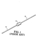
- Fig. 1 shows a conventional semiconductor device package 10 with a specification of DO-41.
- the conventional semiconductor device package 10 has a length in the range of 4.06mm-5.21mm and a diameter in the range of 2.03-2.72mm.
- Two leads 15 on both sides of the semiconductor device package 10 each has a length of approximately 27.94mm and a diameter in the range of 0.71-0.86mm.
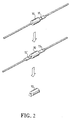
- Fig. 2 is a schematic view showing the steps of processing conventional semiconductor device package leads by an automatic machine.
- part of one lead 15 adjacent to the semiconductor device package 10 is first flattened, and then part of the other lead 15' adjacent to the semiconductor device package 10 is flattened.
- the remaining parts of the two leads 15 and 15' which are not flattened, are cut off.
- the flattened parts of the two leads 15 and 15' are bent.
- the above-stated two-stage flattening step (one stage is to flatten one lead and the other stage is to flatten the other lead) can prevent internal component of the semiconductor device package 10 from damage.
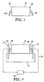
- Fig. 3 is a side view showing a semiconductor device package 35 having non-soldered leads 30 and 30' according to the invention.
- the length of leads 30 and 30' have been trimmed to be at the same level with the periphery of the side surfaces 38 and 38' of the semiconductor device package 35. Furthermore, there is a small angle formed between each bent lead 30 and a corresponding side surface of the semiconductor device package 35 for a better elastic contact with a circuit.
- Fig. 4 is a semiconductor device package according to the invention assembled to a circuit 48.
- the semiconductor device package 35 is mounted on a carrier 44, wherein the two flattened and bent leads 30 and 30' are elastically engaged with two copper plates 42 respectively.
- the semiconductor device package 35 is electrically connected to the circuit 48 via the two copper plates 42 and a wire 46.
Landscapes
- Lead Frames For Integrated Circuits (AREA)
Priority Applications (1)
| Application Number | Priority Date | Filing Date | Title |
|---|---|---|---|
| EP98310154A EP1005084A1 (de) | 1998-11-17 | 1998-12-11 | Halbleiterverpackung mit Anschlüssen zur lötfreien Kontaktierung |
Applications Claiming Priority (2)
| Application Number | Priority Date | Filing Date | Title |
|---|---|---|---|
| 1998-11-17 | |||
| EP98310154A EP1005084A1 (de) | 1998-11-17 | 1998-12-11 | Halbleiterverpackung mit Anschlüssen zur lötfreien Kontaktierung |
Publications (1)
| Publication Number | Publication Date |
|---|---|
| EP1005084A1 true EP1005084A1 (de) | 2000-05-31 |
Family
ID=8235203
Family Applications (1)
| Application Number | Title | Priority Date | Filing Date |
|---|---|---|---|
| EP98310154A Withdrawn EP1005084A1 (de) | 1998-11-17 | 1998-12-11 | Halbleiterverpackung mit Anschlüssen zur lötfreien Kontaktierung |
Country Status (1)
| Country | Link |
|---|---|
| EP (1) | EP1005084A1 (de) |
Citations (2)
| Publication number | Priority date | Publication date | Assignee | Title |
|---|---|---|---|---|
| JPS6081851A (ja) * | 1983-10-12 | 1985-05-09 | Nec Corp | Icケ−ス |
| EP0225238A1 (de) * | 1985-11-08 | 1987-06-10 | Thomson Composants Militaires Et Spatiaux | Karten mit einem Bauelement und Mikromodul mit Seitenkontakten |
-
1998
- 1998-12-11 EP EP98310154A patent/EP1005084A1/de not_active Withdrawn
Patent Citations (2)
| Publication number | Priority date | Publication date | Assignee | Title |
|---|---|---|---|---|
| JPS6081851A (ja) * | 1983-10-12 | 1985-05-09 | Nec Corp | Icケ−ス |
| EP0225238A1 (de) * | 1985-11-08 | 1987-06-10 | Thomson Composants Militaires Et Spatiaux | Karten mit einem Bauelement und Mikromodul mit Seitenkontakten |
Non-Patent Citations (2)
| Title |
|---|
| "Three-dimensional module power and signal distribution mechanism", IBM TECHNICAL DISCLOSURE BULLETIN., vol. 27, no. 10A, March 1985 (1985-03-01), NEW YORK US, pages 5564 - 5565, XP002105011 * |
| PATENT ABSTRACTS OF JAPAN vol. 009, no. 225 (E - 342) 11 September 1985 (1985-09-11) * |
Similar Documents
| Publication | Publication Date | Title |
|---|---|---|
| US5600178A (en) | Semiconductor package having interdigitated leads | |
| EP0657931B1 (de) | Verfahren zur Herstellung einer Halbleitervorrichtung | |
| US5057805A (en) | Microwave semiconductor device | |
| US6191951B1 (en) | Smart card module and smart card including a smart card module | |
| US6465276B2 (en) | Power semiconductor package and method for making the same | |
| US9806010B2 (en) | Package module and method of fabricating the same | |
| US5451716A (en) | Resin-packaged electronic component having bent lead terminals | |
| EP0978871A2 (de) | Ein Packungsentwurf für eine Anordnung niedriger Leistung | |
| KR100429319B1 (ko) | 유기기판을가진전자부품을제조하기위한방법 | |
| US6593658B2 (en) | Chip package capable of reducing moisture penetration | |
| US6833512B2 (en) | Substrate board structure | |
| US20090045491A1 (en) | Semiconductor package structure and leadframe thereof | |
| US6417576B1 (en) | Method and apparatus for attaching multiple metal components to integrated circuit modules | |
| US6395982B2 (en) | Leaded semiconductor device package for use in nonsoldering assembling | |
| EP1005084A1 (de) | Halbleiterverpackung mit Anschlüssen zur lötfreien Kontaktierung | |
| EP0907307A1 (de) | Wärmesenke für oberflächenmontierte Leistungspackungen | |
| US4963975A (en) | Semiconductor device | |
| JP3428475B2 (ja) | 半導体パッケージの製造方法 | |
| US7205574B2 (en) | Optical semiconductor device | |
| JP2901941B2 (ja) | 高周波電力用半導体装置 | |
| KR20020075280A (ko) | 반도체 장치 | |
| US6600216B1 (en) | Structure of a pin platform for integrated circuit | |
| JP2788899B2 (ja) | 表面実装用集積回路 | |
| US20260020205A1 (en) | Shielding combining press-fit with surface mount compression | |
| JP3157249B2 (ja) | 半導体装置実装体及び実装方法 |
Legal Events
| Date | Code | Title | Description |
|---|---|---|---|
| PUAI | Public reference made under article 153(3) epc to a published international application that has entered the european phase |
Free format text: ORIGINAL CODE: 0009012 |
|
| AK | Designated contracting states |
Kind code of ref document: A1 Designated state(s): AT BE CH CY DE DK ES FI FR GB GR IE IT LI LU MC NL PT SE |
|
| AX | Request for extension of the european patent |
Free format text: AL;LT;LV;MK;RO;SI |
|
| 17P | Request for examination filed |
Effective date: 20000713 |
|
| AKX | Designation fees paid |
Free format text: AT BE CH CY DE DK ES FI FR GB GR IE IT LI LU MC NL PT SE |
|
| AXX | Extension fees paid |
Free format text: AL PAYMENT 20000713;LT PAYMENT 20000713;LV PAYMENT 20000713;MK PAYMENT 20000713;RO PAYMENT 20000713;SI PAYMENT 20000713 |
|
| STAA | Information on the status of an ep patent application or granted ep patent |
Free format text: STATUS: THE APPLICATION IS DEEMED TO BE WITHDRAWN |
|
| 18D | Application deemed to be withdrawn |
Effective date: 20060912 |