EP0999599A2 - Infrarotphotodetektor mit optischem Resonator - Google Patents
Infrarotphotodetektor mit optischem Resonator Download PDFInfo
- Publication number
- EP0999599A2 EP0999599A2 EP99250287A EP99250287A EP0999599A2 EP 0999599 A2 EP0999599 A2 EP 0999599A2 EP 99250287 A EP99250287 A EP 99250287A EP 99250287 A EP99250287 A EP 99250287A EP 0999599 A2 EP0999599 A2 EP 0999599A2
- Authority
- EP
- European Patent Office
- Prior art keywords
- contact
- quantum well
- elements
- multiple quantum
- array
- Prior art date
- Legal status (The legal status is an assumption and is not a legal conclusion. Google has not performed a legal analysis and makes no representation as to the accuracy of the status listed.)
- Withdrawn
Links
Images



Classifications
-
- B—PERFORMING OPERATIONS; TRANSPORTING
- B82—NANOTECHNOLOGY
- B82Y—SPECIFIC USES OR APPLICATIONS OF NANOSTRUCTURES; MEASUREMENT OR ANALYSIS OF NANOSTRUCTURES; MANUFACTURE OR TREATMENT OF NANOSTRUCTURES
- B82Y20/00—Nanooptics, e.g. quantum optics or photonic crystals
-
- H—ELECTRICITY
- H10—SEMICONDUCTOR DEVICES; ELECTRIC SOLID-STATE DEVICES NOT OTHERWISE PROVIDED FOR
- H10F—INORGANIC SEMICONDUCTOR DEVICES SENSITIVE TO INFRARED RADIATION, LIGHT, ELECTROMAGNETIC RADIATION OF SHORTER WAVELENGTH OR CORPUSCULAR RADIATION
- H10F39/00—Integrated devices, or assemblies of multiple devices, comprising at least one element covered by group H10F30/00, e.g. radiation detectors comprising photodiode arrays
- H10F39/10—Integrated devices
- H10F39/12—Image sensors
- H10F39/18—Complementary metal-oxide-semiconductor [CMOS] image sensors; Photodiode array image sensors
- H10F39/184—Infrared image sensors
- H10F39/1843—Infrared image sensors of the hybrid type
-
- H—ELECTRICITY
- H10—SEMICONDUCTOR DEVICES; ELECTRIC SOLID-STATE DEVICES NOT OTHERWISE PROVIDED FOR
- H10F—INORGANIC SEMICONDUCTOR DEVICES SENSITIVE TO INFRARED RADIATION, LIGHT, ELECTROMAGNETIC RADIATION OF SHORTER WAVELENGTH OR CORPUSCULAR RADIATION
- H10F39/00—Integrated devices, or assemblies of multiple devices, comprising at least one element covered by group H10F30/00, e.g. radiation detectors comprising photodiode arrays
- H10F39/80—Constructional details of image sensors
- H10F39/805—Coatings
Definitions
- the present invention pertains in general to infrared detectors and in particular to such detectors which utilize quantum well infrared photodetector elements having an optical cavity enhancement coating thereon.
- the current objectives are to provide technology for large area focal plane arrays for long wave infrared radiation (LWIR), multispectral applications, and to provide this technology at low cost with high performance.
- Substantial performance has been shown by second generation photovoltaic (PV) mercury cadmium telluride (MCT) diode technology.
- PV photovoltaic
- MCT mercury cadmium telluride
- This technology has significant producability and uniformity advantages over second generation PV MCT technology. This is primarily because it is based on mature GaAs/AlGaAs material and processing technology.
- QWIP technology suffers from a performance disadvantage in comparison to second generation PV MCT technology.
- a primary performance problem with QWIP technology is the requirement for a substantially higher bias voltage for operation which results in the production of a large dark current. The large dark current lowers the sensitivity (D*) of the detector. The excessively large dark current also severely limits the sensitivity of the detector when used within a focal plane array (FPA).
- Another performance problem with QWIP technology is reduced quantum efficiency relative to PV MCT technology.
- the present invention has the advantages of increased signal output and decreased noise.
- a selected embodiment of the present invention is a quantum well infrared radiation photodetector which includes a plurality of elongate, multiple quantum well infrared radiation absorbing elements, each of which has a first and a second opposite longitudinal surface.
- the configuration of multiple quantum well elements comprises a diffraction grating for the infrared radiation.
- a first contact includes a plurality of planar, electrically connected strips which are respectively in contact with and extending along the first surfaces of the multiple quantum well elements.
- a second contact is electrically connected to the second surfaces of the multiple quantum well elements. The first contact and the second contact are positioned on opposite longitudinal sides of each of the multiple quantum well elements to provide current flow through the elements in a direction substantially transverse to the axis of the elements.
- a planar reflector for said infrared radiation is included.
- the reflector is positioned on an opposite side of the second contact from the multiple quantum well elements.
- An optical cavity enhancement coating is applied to the surfaces of photodetector between the wells.
- the optical cavity enhancement coating completely fills the space between the elongate quantum well elements and has a planar surface perpendicular to the axis of the surface of the quantum wells.
- an optical cavity enhancement coating which completely fills the voids between the elements has an index of refraction of 1.5 or less.
- refractive index means the refractive index of the material to the wavelength the detector is designed to receive.
- the second contact has either a planar configuration or it comprises a plurality of electrically interconnected strips in contact with and extending along the second surfaces of the multiple quantum well elements.
- the optical cavity enhancement coating completely fills the space between the quantum well elements and extends above the first contact and forms a planar top surface over the detector.
- Optical cavity enhancement coatings which do not completely fill the space between the walls should have a refractive index of 2.5 or less and preferably 2.0 or less.
- the present invention in another embodiment includes a detector having an applied optical cavity enhancement coating which has a planar surface and the application of an anti-reflective coating over the optical cavity enhancement coating.
- a QWIP 20 receives incident mode infrared radiation as indicated by arrow 22. Reflected zero order diffractive mode radiation is indicated by arrows 24. Trapped higher order diffractive mode radiation is indicated by arrows 26.
- the QWIP 20 includes a GaAs substrate 30 which is joined to an AlAs reflector 32. An n + GaAs contact 34 is joined to the reflector 32 and to an MQW region 36 comprising a group of layers. A metal diffractive grating 38 is joined to the MQW region. Because of quantum mechanical selection rules an MQW only absorbs radiation through modes in which a component of the electric field is perpendicular to the MQW layers in the MQW region 36.
- the purpose of the grating 38 is to increase the absorption of radiation by diffracting that radiation, as indicated by arrow 22, by the grating 38 to produce trapped diffracting radiation modes shown by the arrows 26 with electric field component perpendicular to the MQW region.
- the arrows 26 represent trapped radiation. Only the radiation reflected normal to the surface of the QWIP 20, as shown by arrows 24, is lost by the QWIP 20.
- the addition of the metal grating 38 increases the absorption of infrared radiation by the QWIP 20.
- a QWIP 40 similar to that shown in Figure 1, has incident mode radiation indicated by arrow 22, reflected zero order diffractive mode radiation indicated by arrows 24 and trapped higher order diffractive mode radiation indicated by arrows 26.
- the QWIP 40 includes a thin GaAs substrate 42, an n + contact 44, MQW region 46 and a metal grating 48.
- QWIPs 36 and 46 shown in Figures 1 and 2 each comprise approximately a 50 period GaAs/Al x Ga 1-x As MQW with 40-50 A GaAs wells doped n-type with a doping density of N D ⁇ (0.7-1.5)x10 18 cm -3 and 300-500 A undoped Al x Ga 1-x As barrier.
- the Aluminum to Gallium alloy ratio, x is typically 0.26-0.29 for LWIR application.
- the MQW region 36 and 46 includes an MQW sandwiched between two highly doped n-type (N D ⁇ 2x10 18 cm -3 ) n + GaAs contact layers with typical thicknesses of 0.5-1 ⁇ m.
- the QWIP structure is epitaxially grown on a lattice matched GaAs substrate.
- Figures 1-8 appear in U.S. Patent No. 5,539,206 except that they may contain additional reference numerals, and illustrate infrared photodetector constructions used in making the present invention.
- FIG. 3A A sequence of processing steps for fabricating a detector without the anti-reflective coating is shown in Figures 3A, 3B, 3C and 3D.
- a detector 60 is fabricated on a GaAs substrate 62 with a thickness of approximately 635 ⁇ m.
- An Al .6 Ga .4 As etch stop layer 64 is formed on the surface of the substrate 62.
- the layer 64 has a preferable thickness of 1,000 ⁇ .
- a conductive n + GaAs contact 66 is formed on the etch stop layer 64.
- the contact 66 has a preferable thickness of 0.5 ⁇ m.
- a multiple quantum well (MQW) structure 68 is formed over the contact 66.
- Structure 68 comprises a plurality of material layers which make up the MQW. The detailed characteristics of structure 68 are shown in Table I below.
- An n + GaAs contact 70 is formed on the upper surface of the structure 68. Contact 70 has a preferred thickness of 0.4 ⁇ m.
- openings 76 and 78 are formed by etching through the contact 70 and MQW structure 68.
- the detector 60 has an etched, planar Au/Ge ohmic contact 74 formed on the surface of the contact 70.
- An Au contact/reflector 72 which is a reflector for infrared radiation, is formed on the surface of contact 70 and contact 74.
- an In (indium) bump 80 is bonded to the reflector 72 and to a contact terminal (not shown) of a silicon readout integrated circuit (ROIC) 81.
- the bump 80 is formed by a photoresist image reversal process followed by In layer deposition and liftoff A wicked epoxy 83 provides a physical bond between the ROIC 81, the bump 80 and the remaining exposed structure of the detector 60.
- FIG. 3C Further processing of the detector 60 is shown in Figure 3C.
- the structure shown in Figure 3C is inverted from that shown in Figure 3B.
- the bulk of the substrate 62 is removed by lapping and the remainder is removed by etching down to the etch stop layer 64.
- the layer 64 itself is then removed.
- Contact 66 is thinned from 0.5 ⁇ m to 0.4 ⁇ m.
- a conventional resist mask is applied to the surface of the layer 66 and an etch operation is performed. The etch extends through the layer 66, the MQW structure 68 down to the contact 70.
- Elongate structure 84 comprises a contact 66A over an elongate MQW element 68A.
- elongate structure 86 comprises a contact 66B which is in physical and electrical contact with an elongate MQW element 68B
- structure 88 comprises a contact 66C over an MQW element 68C
- structure 90 comprises a contact 66D over an MQW element 68D.
- the elements 84, 86, 88 and 90 are spaced in such a manner as to form a diffraction grating for the infrared radiation to be received by the detector 60. This produces a void or air space between the elements 84, 86, 88, 90 and an air space or void between elements 84 and 82 and between element 90 and structure 92.
- the optical cavity enhancement coating will be placed in these voids so as to partially or completely fill the voids.
- the MQW elements 68A-D are each infrared radiation absorbers.
- the etching process shown in Figure 3D also produces structures 82 and 92.
- the structure 82 comprises an n + GaAs conductor 66E above a region of the epoxy 83.
- the structure 92 comprises an n + GaAs conductor 66F which is supported by a region of the epoxy 83.
- FIG. 4A there is shown a dimensioned layout for a detector 100.
- This represents one pixel element within an array of such elements.
- the detector 100 includes elements 102, 104, 106, 108 and 110 which are formed in the same manner as the elements 84, 86, 88 and 90 shown in Figure 3D.
- Each of the elements includes a top elongate n + GaAs contact, such as 102A, an elongate MQW element 102B and a flat planar n + GaAs contact 112 which is connected to the bottom surface of MQW elements for each of the elements 102-110.
- a metal contact/reflector 114 made of Au and having a thickness of 2,000 ⁇ is formed on the opposite side of the contact 112 from the MQW elements such as 102B.
- Each of the elements 102-110 has a width of 1.2 microns and the elements are spaced at a pitch of 8 microns. This physical configuration is tuned for optimum response to LWIR radiation, which is in the 8-10 micron range. The space between elements is approximately 6.8 microns.
- An ohmic contact 113 is a rectangular, planar structure comprising Au/Ge and having a thickness of approximately 900 ⁇ and dimensions of 5 ⁇ m by 10 ⁇ m.
- the ohmic contact 113 is fabricated on the surface of contact 112 before the formation of reflector 114.
- the ohmic contact 113 provides a good ohmic connection between the contact 112 and the reflector 114.
- FIG. 4B A further embodiment of a detector 120 is shown in Figure 4B. This is essentially the same as the detector 100 shown in Figure 4A, but the etching operation which formed the elements 102-110, is continued until the etching extends through a portion of the lower contact 112, but not the entire thickness of the contact 112. This etching operation produces elements 122, 124, 126, 128 and 130. The width and spacing of these elements is the same as the width and spacing of the elements 102-110 shown in Figure 4A. Again, the elements are spaced apart creating air space or voids between the elements. These voids will likewise provide space for the application of the optical cavity enhancement coating.
- the element 122 includes an elongate n + GaAs contact 122A which is in physical and electrical contact with the upper surface of the elongate MQW element 122B and a lower elongate n + GaAs portion of the contact 112.
- the patterned contact 112 is positioned on the surface of a metal reflector 132, which is essentially the same as the reflector 114 shown in Figure 4A.
- a planar ohmic contact 134 corresponding to the ohmic contact 113 shown in Figure 4A, is formed on the n + GaAs contact 112 at a position to the lower right of the element 130.
- the contact/reflector 132 is then formed.
- the ohmic contact 134 provides a good ohmic connection between the contact 112 and the reflector 132.
- FIG. 4C A further embodiment of a detector 120 is shown in Figure 4C. This is the same as the detector 100 shown in Figure 4A but the etching operation which formed the elements 102-110 is continued until the etching extends through the lower contact 112 except for one region. A region 112A is not removed. This etching produces elements 138, 139, 140, 141 and 142. The width and spacing of these elements is approximately the same as the width and spacing of the elements 102-110 shown in Figure 4A. Like Figure 4A, Figure 4C shows voids or air spaces created between the elements. These air spaces will accommodate the applied optical cavity enhancement coating. The sensitivity of a detector to a given wavelength of infrared radiation is related to the width and spacing of the MQW elements.
- the element 138 includes an elongate upper n + GaAs contact 138A in physical and electrical contact with the upper surface of an elongate MQW element 138B and a lower elongate n + GaAs contact 138C is connected to the lower surface of the MQW element 138B.
- the contact 138C and the corresponding contacts on the other elements are positioned on the surface of a metal contact/reflector 137, which is essentially the same as the reflector 114 shown in Figure 4A.
- a planar ohmic contact 143 corresponding to the ohmic contact 113 shown in Figure 4A, is formed on the n + GaAs contact 112 at the position of the region 112A.
- the contact/reflector 137 is then formed.
- the ohmic contact 143 provides a good ohmic connection between the region 112A, which is connected electrically to all of the other lower contacts, such as 138C, and the reflector 137.
- Figures 4A, 4B and 4C represent section views of the elongate elements 102-110, 122-130 and 138-142.
- a focal plane detector array 150 which includes a plurality of detectors as described above arranged in an array.
- a view of the detector array 150 as indicated by the arrows 152 corresponds substantially to the views shown in Figures 3D and 4A.
- the detector array 150 includes detector pixel structures 154, 156, 158, 160, 162 and 164.
- Each pixel structure 154-164 has a corresponding In bump such as bump 166 for pixel structure 154, bump 168 for pixel structure 158, bump 170 for pixel structure 162 and bump 172 for pixel structure 164.
- Each of the bumps is connected to a corresponding terminal (not shown) of a ROIC 180.
- a wicked epoxy 182 bonds the pixel structures 154-164 to the ROIC 180.
- the pixel structure 158 is described in detail. The remaining pixel structures have a similar configuration.
- the entire top surface of the detector array 150 comprises an upper array n + GaAs contact 186 which has been etched to have elongate (strip) segments including 186A and 186B which extend between wider elongate n + GaAs conductors 186C and 186D.
- Elongate segments in pixel structure 158 include segments 186E, 186F, 186G and 186H.
- the segments 186E-186H are each connected at a common end to a wide n + GaAs conductor 186J and a similar conductor (not shown) at the opposite side of the pixel structure 158.
- the contact segments 186A and 186B are transverse to the contact segments 186E, 186F, 186G and 186H.
- Contact segments 186E-186H correspond to contacts 66A, 66B, 66C and 66D in Figure 3D.
- the n + GaAs conductors 186C and 186D correspond to conductors 66E and 66F in Figure 3D.
- Each of the pixel structures 154-164 has a contact/reflector for electrically connecting the lower contact of the pixel to the corresponding In bump.
- the region between the bumps is filled with wicked epoxy 182, such as shown in Figures 3C and 3D.
- each of the pixel structures 154-164 immediately below the n + GaAs contact 186 is a diffractive MQW structure 190 which has a segment beneath each of the contact 186 segments. This is essentially the same as shown in Figures 3D and 4A.
- MQW element 190A is immediately below contact 186A.
- a planar contact is formed in a position between the MQW structure 190 and a contact/reflector.
- the pixel structures 154, 156, 158, 160, 162 and 164 have respective lower (second) contacts 194A, 194B, 194C, 194D, 194E and 194F.
- a contact/reflector 196A is in a lower portion of pixel structure 154. Reflector 196A is physically and electrically in contact with bump 166. A contact/reflector 196B is in the lower portion of pixel structure 158 and is in electrical contact with the bump 168. A contact/reflector 196C is in the lower portion of pixel structure 162 and a contact/reflector 196D is in the lower portion of pixel structure 164.
- the contacts/reflectors are made preferably of Au and have a preferred thickness of 2,000 ⁇ . Reflectors 196A-196D correspond to reflector 72 in Figure 3D.
- Slots 210, 212, 214, 216 and 218 are etched into the structure of detector 150 to electrically isolate each pixel structure. Each of these slots extends upward from the region occupied by the bumps up to the lower surface of the contact 186. These slots are filled with the epoxy 182, which is electrically nonconductive.
- the result of the fabrication is a series of square channels formed by the EQWIP elements and the slots, giving the detector an eggcrate appearance.
- Each of the pixel structures 154, 156, 158, 160, 162 and 164 has 25 sections (5 by 5) and has generally at the base of one section a rectangular, planar ohmic contact, such as ohmic contact 219 shown for pixel structure 164.
- the ohmic contact can extend to have an area greater than that of one section.
- the ohmic contact 219 is made of Au/Ge and is positioned between the lower n + GaAs contact 194F and the Au reflector 196D.
- the ohmic contact 219 provides an ohmic connection between the n + GaAs contact 194F and the reflector 196D.
- a similar ohmic contact is provided at a similar location in each of the other pixel structures.
- Each of the contacts/reflectors provides an electrical connection to the corresponding bump beneath the detector pixel structure.
- Each contact/reflector also functions as an infrared radiation reflector.
- the detector array 150 is fabricated by use of the materials and steps described in reference to Figures 3A-3D. Parameters for the detector array 150, as shown in Figure 5, are set out in Table I below. The test results shown in Table II is for a detector in which the pixel size is 56 ⁇ m x 56 ⁇ m and a typical pixel spacing in the array is 60 ⁇ m x 60 ⁇ m.
- the top contact 186 is connected to through-conductors on the periphery outside the pixel structures. These through-conductors extend down to In bumps, as described above, to terminals of the underlying ROIC.
- the detector array 150 shown in Figure 5 is non-polarized because the MQW diffractive grating elements are transverse to each other within each pixel structure. Therefore, all polarizations of incident infrared radiation are received.
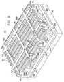
- a polarized detector array 240 which is similar to the detector array 150 shown in Figure 5, but has elongate diffractive MQW elements extending in only one direction.
- the detector array 240 includes detector pixel structures 242, 244, 246, 248, 250 and 252.
- Each pixel structure has a corresponding In bump for connection to an ROIC 260.
- Bump 262 connects pixel structure 242 to a terminal (not shown) of ROIC 260.
- Each pixel structure therefore generates a different signal which is provided to the ROIC 260.
- the space between the bumps 262-268 is filled with wicked epoxy 270 for bonding the surrounding elements together.
- the detector array 240 has a layer comprising an n + GaAs array contact 274 on the upper surface thereof which comprises a plurality of elongate contact strips, all of which are electrically and physically interconnected to each other.
- the pixel structure 246 has elongate contacts 274A and 274B.
- the pixel structure 246 includes MQW elements 276A and 276B, which have the n + GaAs strip contacts 274A and 274B on the upper surfaces thereof.
- the contact strips 274A and 274B extend between wider n + GaAs conductors 274C and 274D.
- a lower (second) planar n + GaAs contact for each pixel structure extends across the detector 240 but is divided into separate contacts for each of the pixel structures. This consists of contact 280A for structure 242, contact 280B for structure 244, contact 280C for structure 246, contact 280D for structure 248, contact 280E for structure 250 and contact 280F for structure 252.
- Contact 280 corresponds to the contact 70 shown in Figures 3A-3D.
- the contacts 280A-F are separated by slots 282, 284, 286, 288 and 290.
- the resulting structure has elongate channels 380 formed by the EQWIP elements and the slots.
- An Au contact/reflector is also divided by the slots 282-290 in individual contact/reflectors corresponding to each pixel structure.
- Pixel structure 242 has reflector 298A
- structure 246 has reflector 298B
- structure 250 has reflector 298C
- pixel structure 252 has reflector 298D.
- each of the reflectors provides an electrical connection to the corresponding bump beneath the pixel structure.
- Each reflector also functions as an infrared radiation reflector.
- Each of the pixel structures 242, 244, 246, 248, 250 and 252 has five longitudinal sections and one longitudinal section thereof is provided with an ohmic contact, such as ohmic contact 292 shown for pixel structure 250 and contact 294 shown for pixel structure 252.
- Each ohmic contact is a rectangular structure comprising Au/Ge having a thickness of 900 ⁇ .
- Each ohmic contact is formed between the corresponding lower contact, such as contact 280E for pixel structure 250 and the underlying reflector 298C.
- the ohmic contact provides a good ohmic connection between the overlying second n + GaAs contact and the underlying Au reflector.
- the detector array 240 shown in Figure 6 has elongate MQW elements running in only one direction. It is therefore sensitive to only one polarity of infrared radiation.
- a focal plane array 310 which comprises a plurality of pixel structures.
- This array preferably has 640 pixel structures horizontally and 480 pixel structures vertically.
- Each of the pixel structures within the array 310 has a separate electrical output signal so that a complete image having 640 x 480 elements can be produced.
- a top n + GaAs contact such as contact 186, is connected to an electrically common point which is shown by a ground symbol.
- a particular diffractive MQW element 320 which corresponds, for example, to the diffractive MQW element 190A, is connected between the top contact 186 and the lower contact, which corresponds to n + GaAs contact 194C.
- the lower contact is ohmically connected to the Au reflector 196B and connected through the bump 168 to the ROIC 180. For a preferred embodiment this is a "direct injection" ROIC.
- the signal transmitted through the bump 168 is provided to a MOSFET PREAMP transistor 322 which has a gate terminal connected to a V bias supply.
- Transistor 322 functions as a preamplifier.
- the amplified signal produced by transistor 322 is integrated by a capacitor 324.
- the integrated signal is provided to a multiplexer (not shown) which selectively samples the signal produced by each of the pixel structures throughout the array.
- the MQW element 320 is provided with the noted bias voltage through the transistor 322 and intervening conductors to the MQW element 320.
- each of the MQW elements described above has a linear configuration, such elements may also have a curved and elongate configuration.
- the QWIP structure describes enhanced performance for receiving infrared radiation without an optical cavity enhancement coating.
- the upper and lower contact connections on opposite longitudinal surfaces provides current flow transverse to the axis to the elongate, diffractive MQW elements.
- the elongate, diffractive MQW elements produce less dark current in proportion to the MQW cross-sectional area than a conventional QWIP in which the MQW is unpatterned. It has been discovered that the spacing between the elements exposes the elements to air and permits leakage current. This surface leakage current along the surface creates additional noise which degrades performance.
- an optical cavity enhancement coating the surface current is reduced and therefore noise in the detection signal can be reduced, enhancing performance.
- the optical cavity enhancement coating is applied in the preferred embodiment so as to fill the space between the elements.
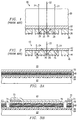
- Figure 9A corresponds to Figure 4B, but in addition shows an optical cavity enhancement coating 390 applied in the space between the elements 122, 124, 126, 128 and 130 so as to cover the longitudinal surfaces of the elements. Filling the air space (voids) between the elements is beneficial if the proper material is utilized.
- the optical cavity enhancement coating should be of a material with a refractive index of 1.5 or less.
- the index of refraction of the optical cavity enhancement coating is important because if it is too high, the electromagnetic energy field will be concentrated in both the absorbing quantum well portion of the EQWIP material as well as the in the coating located between the voids. Since the detector utilizes only the energy collected in the absorbing quantum well portion of the EQWIP material, energy concentration in the optical cavity enhancement coating should be minimized.
- Figure 9B shows the resulting structure of the preferred embodiment in which the entire space between the elements 122, 124, 126, 128 and 130 is filled with optical cavity enhancement coating 400 and the coating extends above the n+ contacts 122A. It is desirable that the thickness T above the contacts be in the range of 1 to 3 microns.
- Figure 9B also corresponds to Figure 4B but illustrates a different configuration of the optical cavity enhancement coating which also forms an overcoat over the entire array structure.
- an anti-reflective coating 402 can be applied to the planar surface of the optical cavity enhancement coating 400.
- Anti-reflective coatings are known in art and will not be described further.
- the optical cavity enhancement coating can be applied in a similar fashion to the embodiments illustrated in Figures 4A and 4C.
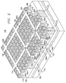
- Figure 10 is a partial view of the focal plane detector array 150 including an overcoat of optical cavity enhancement material 404.
- the view of the array is indicated by arrow 152 and corresponds to views shown in Figures 3D and 4A, with the exception of the addition of the optical cavity enhancement coating.
- the optical cavity enhancement coating in the illustrated embodiment shows an overcoat that extends above the elements composed of the various elongate MQW element and the n+ contacts, generally indicated as 406.
- the outer surface of the optical cavity enhancement coating is smooth and follows the shape of the outer edges of the array. For ease of illustration, a planar array is shown and thus the overcoat would preferably have a flat top surface.
- the optical cavity enhancement overcoat may be a suitable plastic such as polyimide which is spun onto the device during fabrication.
- the polyimide may be applied by spinning the polyimide onto the detector. In this method, the polyimide is applied to the detector as a liquid and then the detector is placed on the turntable. The turntable is spun throwing off the excess polyimide. The thickness of the polyimide remaining can be controlled by variations in the viscosity of the liquid and by the rpms of the turntable. Thereafter, the polyimide is cured. Curing is usually accomplished by heating the polyimide to a suitable temperature. The curing temperature will vary depending on the particular polyimide.
- the coating material can have a refractive index of 2.5 or less and preferably 2.0 or less.
- the proper selection of the refractive index of the coating will result in the concentration of energy in the quantum well portion of the EQWIP material, although some energy will be in the coating. Concentrating the majority of the energy in the EQWIP material increases the response signal for the incident energy.
- the optical cavity enhancement can also be a dielectric having a refractive index as specified such as SiO 2 or Si 3 N 4 .
- the SiO 2 or Si 3 N 4 may be applied by any suitable technique known in the art such as evaporation.
- the optical cavity enhancement coating does not completely fill the space or void between the elements.
- the coating 410 may be a conforming covering which mirrors the shape of the array without the coating.
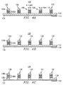
- the surfaces of elements 140, 141, 142 are covered with the optical cavity enhancement coating.
- the coating is shown extending only to element 139.
- Figure 11 corresponds to Figure 4c.
- the same technique may be used to provide a optical cavity enhancement coating to the embodiments illustrated in Figures 4a and 4b.
- the coating will cover the longitudinal surfaces of the elements as well as the reflector or lower contact as the case may be.
- an enhancement coating material having a higher refractive index may be utilized.
- the refractive index can be 2.5 or less and preferably is 2.0 or less.
- the thickness of the conformable coating which does not fill the void is selected in conjunction with the refractive index of the coating material and the wavelength the detector is designed to detect. The refractive index and the thickness of the coating can be adjusted so as to achieve maximum resonance for the wavelength the detector is designed to detect. .
- the optical cavity enhancement coating can be any non-conductive material having a suitable index of refraction and which is compatible, i.e., does not degradate the materials used to construct the detector.
- the indices of refraction in the 8-12 micron wavelength region for suitable coatings are: Polyimide 1.5 SiO 2 about 0.45 (but varying) Si 3 N 4 2.0 ZnS 2.2
- FIG. 9A, 9B, 10 and 11 are not to scale for purposes of illustration.
- the present invention has been described using a Gallium Arsenide/Aluminum Gallium Arsenide MQW operating in the long wave infrared spectral band of 8-10 ⁇ m. However, through the proper selection of parameters and of MQW material systems, the invention is applicable to others spectral bands. Alternate MQW material systems include but are not limited to Indium Gallium Arsenide/Indium Aluminum Arsenide, Indium Gallium Arsenide/Indium Phosphide and strained Indium Gallium Arsenide/Gallium Arsenide.
Landscapes
- Chemical & Material Sciences (AREA)
- Engineering & Computer Science (AREA)
- Nanotechnology (AREA)
- Physics & Mathematics (AREA)
- Life Sciences & Earth Sciences (AREA)
- Biophysics (AREA)
- Optics & Photonics (AREA)
- Crystallography & Structural Chemistry (AREA)
- Light Receiving Elements (AREA)
- Photometry And Measurement Of Optical Pulse Characteristics (AREA)
- Solid State Image Pick-Up Elements (AREA)
Applications Claiming Priority (2)
| Application Number | Priority Date | Filing Date | Title |
|---|---|---|---|
| US09/185,249 US6157042A (en) | 1998-11-03 | 1998-11-03 | Optical cavity enhancement infrared photodetector |
| US185249 | 1998-11-03 |
Publications (2)
| Publication Number | Publication Date |
|---|---|
| EP0999599A2 true EP0999599A2 (de) | 2000-05-10 |
| EP0999599A3 EP0999599A3 (de) | 2003-08-06 |
Family
ID=22680218
Family Applications (1)
| Application Number | Title | Priority Date | Filing Date |
|---|---|---|---|
| EP99250287A Withdrawn EP0999599A3 (de) | 1998-11-03 | 1999-08-25 | Infrarotphotodetektor mit optischem Resonator |
Country Status (4)
| Country | Link |
|---|---|
| US (1) | US6157042A (de) |
| EP (1) | EP0999599A3 (de) |
| JP (1) | JP5027960B2 (de) |
| NO (1) | NO995342L (de) |
Families Citing this family (27)
| Publication number | Priority date | Publication date | Assignee | Title |
|---|---|---|---|---|
| US6561693B1 (en) * | 2000-09-21 | 2003-05-13 | Lockheed Martin Corporation | Remote temperature sensing long wave length modulated focal plane array |
| US6828545B1 (en) * | 2001-05-15 | 2004-12-07 | Raytheon Company | Hybrid microelectronic array structure having electrically isolated supported islands, and its fabrication |
| US6593666B1 (en) * | 2001-06-20 | 2003-07-15 | Ambient Systems, Inc. | Energy conversion systems using nanometer scale assemblies and methods for using same |
| US6689628B1 (en) | 2002-08-15 | 2004-02-10 | Bae Systems Information And Electronic Systems Integration Inc. | Method for dense pixel fabrication |
| US7135698B2 (en) * | 2002-12-05 | 2006-11-14 | Lockheed Martin Corporation | Multi-spectral infrared super-pixel photodetector and imager |
| US6897447B2 (en) * | 2002-12-05 | 2005-05-24 | Lockheed Martin Corporation | Bias controlled multi-spectral infrared photodetector and imager |
| US7148579B2 (en) | 2003-06-02 | 2006-12-12 | Ambient Systems, Inc. | Energy conversion systems utilizing parallel array of automatic switches and generators |
| US7199498B2 (en) * | 2003-06-02 | 2007-04-03 | Ambient Systems, Inc. | Electrical assemblies using molecular-scale electrically conductive and mechanically flexible beams and methods for application of same |
| US7095645B2 (en) * | 2003-06-02 | 2006-08-22 | Ambient Systems, Inc. | Nanoelectromechanical memory cells and data storage devices |
| US20040238907A1 (en) * | 2003-06-02 | 2004-12-02 | Pinkerton Joseph F. | Nanoelectromechanical transistors and switch systems |
| US7214195B2 (en) * | 2003-07-23 | 2007-05-08 | Lockheed Martin Corporation | Method of and apparatus for detecting diseased tissue by sensing two bands of infrared radiation |
| US7518283B2 (en) | 2004-07-19 | 2009-04-14 | Cjp Ip Holdings Ltd. | Nanometer-scale electrostatic and electromagnetic motors and generators |
| WO2006044983A2 (en) * | 2004-10-20 | 2006-04-27 | Massachusetts Institute Of Technology | Multi-spectral pixel and focal plane array |
| CN101199056B (zh) * | 2005-06-14 | 2011-04-20 | 皇家飞利浦电子股份有限公司 | 多视图显示装置 |
| WO2008124084A2 (en) | 2007-04-03 | 2008-10-16 | Pinkerton Joseph F | Nanoelectromechanical systems and methods for making the same |
| FR2937791B1 (fr) * | 2008-10-24 | 2010-11-26 | Thales Sa | Dispositif d'imagerie polarimetrique optimise par rapport au contraste de polarisation |
| EP2264765A1 (de) * | 2009-06-19 | 2010-12-22 | Fraunhofer-Gesellschaft zur Förderung der angewandten Forschung e.V. | Gehäuse für eine Infrarot-Mikrovorrichtung und Verfahren zur Herstellung eines solchen Gehäuses |
| US8608894B2 (en) * | 2010-11-23 | 2013-12-17 | Raytheon Company | Wafer level packaged focal plane array |
| WO2013066447A1 (en) | 2011-08-01 | 2013-05-10 | The Trustees Of Columbia University In The City Of New York | Lens-free planar imager and wireless transmitter |
| WO2013059665A1 (en) | 2011-10-19 | 2013-04-25 | The Trustees Of Columbia University In The City Of New York | Ultracompact fabry-perot array for ultracompact hyperspectral imaging |
| US9373732B2 (en) | 2012-02-07 | 2016-06-21 | Semiconductor Components Industries, Llc | Image sensors with reflective optical cavity pixels |
| WO2013148349A1 (en) | 2012-03-30 | 2013-10-03 | The Trustees Of Columbia University In The City Of New York | Graphene photonics for resonator-enhanced electro-optic devices and all-optical interactions |
| US9252182B2 (en) | 2012-09-05 | 2016-02-02 | Northrop Grumman Systems Corporation | Infrared multiplier for photo-conducting sensors |
| US9212948B2 (en) | 2012-11-07 | 2015-12-15 | The Trustees Of Columbia University In The City Of New York | Lossless hyperspectral imaging |
| US10325947B2 (en) | 2013-01-17 | 2019-06-18 | Semiconductor Components Industries, Llc | Global shutter image sensors with light guide and light shield structures |
| US11121302B2 (en) | 2018-10-11 | 2021-09-14 | SeeQC, Inc. | System and method for superconducting multi-chip module |
| FR3118288B1 (fr) * | 2020-12-23 | 2022-12-30 | Thales Sa | Integration d'un circuit de detection a base de resonateurs optiques interconnectes sur un circuit de lecteure d'un imageur |
Family Cites Families (15)
| Publication number | Priority date | Publication date | Assignee | Title |
|---|---|---|---|---|
| JPS5310861B2 (de) * | 1972-04-26 | 1978-04-17 | ||
| US4578527A (en) * | 1983-11-16 | 1986-03-25 | Optical Coating Laboratory, Inc. | Articles having improved reflectance suppression |
| JPS6413767A (en) * | 1987-07-07 | 1989-01-18 | Fujitsu Ltd | Semiconductor device |
| US4783594A (en) * | 1987-11-20 | 1988-11-08 | Santa Barbara Research Center | Reticular detector array |
| US4936653A (en) * | 1988-06-02 | 1990-06-26 | Santa Barbara Research Center | Cerium oxyfluoride antireflection coating for group II-VI photodetectors and process for forming same |
| JP3249992B2 (ja) * | 1990-12-25 | 2002-01-28 | ミノルタ株式会社 | シリコン基板またはゲルマニウム基板用反射防止膜 |
| US5261970A (en) * | 1992-04-08 | 1993-11-16 | Sverdrup Technology, Inc. | Optoelectronic and photovoltaic devices with low-reflectance surfaces |
| JP2762004B2 (ja) * | 1992-08-28 | 1998-06-04 | ユピテル工業株式会社 | 受光素子 |
| JPH0774385A (ja) * | 1993-09-03 | 1995-03-17 | Hamamatsu Photonics Kk | 静電誘導型アバランシェフォトダイオード |
| JPH0774379A (ja) * | 1993-09-06 | 1995-03-17 | Mitsuteru Kimura | pーn接合フォトセル |
| FR2729789B1 (fr) * | 1993-09-10 | 1998-03-20 | Thomson Csf | Detecteur a puits quantique et procede de realisation |
| US5479032A (en) * | 1994-07-21 | 1995-12-26 | Trustees Of Princeton University | Multiwavelength infrared focal plane array detector |
| US5485015A (en) * | 1994-08-25 | 1996-01-16 | The United States Of America As Represented By The Secretary Of The Army | Quantum grid infrared photodetector |
| US5539206A (en) * | 1995-04-20 | 1996-07-23 | Loral Vought Systems Corporation | Enhanced quantum well infrared photodetector |
| US5777390A (en) * | 1995-10-10 | 1998-07-07 | The University Of Delaware | Transparent and opaque metal-semiconductor-metal photodetectors |
-
1998
- 1998-11-03 US US09/185,249 patent/US6157042A/en not_active Expired - Fee Related
-
1999
- 1999-08-25 EP EP99250287A patent/EP0999599A3/de not_active Withdrawn
- 1999-09-06 JP JP25112499A patent/JP5027960B2/ja not_active Expired - Fee Related
- 1999-11-02 NO NO995342A patent/NO995342L/no not_active Application Discontinuation
Also Published As
| Publication number | Publication date |
|---|---|
| EP0999599A3 (de) | 2003-08-06 |
| JP2000150926A (ja) | 2000-05-30 |
| US6157042A (en) | 2000-12-05 |
| NO995342D0 (no) | 1999-11-02 |
| NO995342L (no) | 2000-05-04 |
| JP5027960B2 (ja) | 2012-09-19 |
Similar Documents
| Publication | Publication Date | Title |
|---|---|---|
| US6157042A (en) | Optical cavity enhancement infrared photodetector | |
| US5539206A (en) | Enhanced quantum well infrared photodetector | |
| EP0999600A2 (de) | Multispektraler Infrarot-Photodetektor | |
| US5773831A (en) | Patch coupled infrared photodetector | |
| EP3864706B1 (de) | Multispektrales photodetektorarray | |
| US6147349A (en) | Method for fabricating a self-focusing detector pixel and an array fabricated in accordance with the method | |
| US8750653B1 (en) | Infrared nanoantenna apparatus and method for the manufacture thereof | |
| US6642537B1 (en) | Dual band QWIP focal plane array | |
| US7238960B2 (en) | QWIP with enhanced optical coupling | |
| US20130087707A1 (en) | Infrared thermal detector and method of manufacturing the same | |
| US6750072B2 (en) | Method for micro-fabricating a pixelless infrared imaging device | |
| US12324269B1 (en) | Wideband detector structures | |
| US6133570A (en) | Semiconductor photovoltaic diffractive resonant optical cavity infrared detector | |
| EP0664052B1 (de) | Impedanzangepasster fotoleitfähiger infrarot-detektor mit heteroübergangskontakten | |
| EP1181724A1 (de) | Wellenlängeunempfindliche strahlungskopplung für mehrfachquantentopf-sensorbasiert auf zwischenunterband-absorption | |
| WO2021001182A1 (en) | Meta-surface photodetector | |
| US20060000974A1 (en) | Polarization and wavelength-selective patch-coupled infrared photodetector | |
| US6828642B2 (en) | Diffraction grating coupled infrared photodetector | |
| KR102588290B1 (ko) | 헬름홀츠 공진기를 가지는 광 검출기 | |
| US5115295A (en) | Photodetector device | |
| GB2241605A (en) | Infrared photodiodes, arrays and their manufacture | |
| CN113447145A (zh) | 一种非制冷氧化钛cmos红外探测器 | |
| Robbins et al. | Silicon-based resonant cavity detectors for long-wave infrared imaging | |
| WO1996010843A1 (en) | Photosensitive semiconductor array |
Legal Events
| Date | Code | Title | Description |
|---|---|---|---|
| PUAI | Public reference made under article 153(3) epc to a published international application that has entered the european phase |
Free format text: ORIGINAL CODE: 0009012 |
|
| AK | Designated contracting states |
Kind code of ref document: A2 Designated state(s): AT BE CH CY DE DK ES FI FR GB GR IE IT LI LU MC NL PT SE |
|
| AX | Request for extension of the european patent |
Free format text: AL;LT;LV;MK;RO;SI |
|
| PUAL | Search report despatched |
Free format text: ORIGINAL CODE: 0009013 |
|
| AK | Designated contracting states |
Designated state(s): AT BE CH CY DE DK ES FI FR GB GR IE IT LI LU MC NL PT SE |
|
| AX | Request for extension of the european patent |
Extension state: AL LT LV MK RO SI |
|
| AKX | Designation fees paid | ||
| REG | Reference to a national code |
Ref country code: DE Ref legal event code: 8566 |
|
| STAA | Information on the status of an ep patent application or granted ep patent |
Free format text: STATUS: THE APPLICATION IS DEEMED TO BE WITHDRAWN |
|
| 18D | Application deemed to be withdrawn |
Effective date: 20040207 |