EP0999596A2 - Sensormatrixanordnung - Google Patents
Sensormatrixanordnung Download PDFInfo
- Publication number
- EP0999596A2 EP0999596A2 EP99308662A EP99308662A EP0999596A2 EP 0999596 A2 EP0999596 A2 EP 0999596A2 EP 99308662 A EP99308662 A EP 99308662A EP 99308662 A EP99308662 A EP 99308662A EP 0999596 A2 EP0999596 A2 EP 0999596A2
- Authority
- EP
- European Patent Office
- Prior art keywords
- photo diode
- guard
- sensors
- array
- diode sensors
- Prior art date
- Legal status (The legal status is an assumption and is not a legal conclusion. Google has not performed a legal analysis and makes no representation as to the accuracy of the status listed.)
- Granted
Links
Images


Classifications
-
- H—ELECTRICITY
- H10—SEMICONDUCTOR DEVICES; ELECTRIC SOLID-STATE DEVICES NOT OTHERWISE PROVIDED FOR
- H10F—INORGANIC SEMICONDUCTOR DEVICES SENSITIVE TO INFRARED RADIATION, LIGHT, ELECTROMAGNETIC RADIATION OF SHORTER WAVELENGTH OR CORPUSCULAR RADIATION
- H10F39/00—Integrated devices, or assemblies of multiple devices, comprising at least one element covered by group H10F30/00, e.g. radiation detectors comprising photodiode arrays
- H10F39/80—Constructional details of image sensors
- H10F39/802—Geometry or disposition of elements in pixels, e.g. address-lines or gate electrodes
Definitions
- This invention relates generally to an array of photo diode sensors.
- it relates to an array of photo diode sensors which include a ring of guard diodes around the periphery of the array.
- An array of image sensors or light sensitive sensors detect the intensity of light received by the image sensors.
- the image sensors typically generate electronic signals that have amplitudes that are proportionate to the intensity of the light received by the image sensors.
- the image sensors convert an optical image into a set of electronic signals.
- the electronic signals may represent intensities of colors of light received by the image sensors.
- the electronic signals can be conditioned and sampled to allow image processing.
- Integration of the image sensors with signal processing circuitry is becoming more important because integration enables miniaturization and simplification of imaging systems. Integration of image sensors along with analog and digital signal processing circuitry allows electronic imaging systems to be low cost, compact and require low power.
- CCDs charged coupled devices
- CCDs are relatively small and can provide a high-fill factor.
- CCDs are very difficult to integrate with digital and analog circuitry.
- CCDs dissipate large amounts of power and suffer from image smearing problems.
- CCD sensors An alternative to CCD sensors are active pixel sensors. Active pixel sensors can be fabricated using standard CMOS processes. Therefore, active pixel sensors can easily be integrated with digital and analog signal processing circuitry. Further, CMOS circuits dissipate small amounts of power.
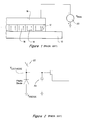
- Figure 1 shows a cross-section of an array of photo diode sensors.
- the array is formed on a substrate 10.
- the array includes photo diode sensors 12, 14, 16. Cathodes of the photo diode sensors 12, 14, 16 are electrically connected to the substrate 10. Anodes of the photo diode sensors 12, 14, 16 are electrically connected to a transparent conductive layer 18.
- the transparent conductive layer 18 is electrically connected to a bias voltage which ensures that the photo diode sensors 12, 14, 16 are reverse biased.
- FIG. 2 is a schematic of a typical circuit included on the substrate 10 which is electrically connected to each photo diode sensor 12, 14, 16.
- the circuit includes a switch 22 which drives the cathode of each photo diode sensor 12, 14, 16 to an initial cathode voltage and charges a cathode capacitor 24.
- the switch 22 is subsequently opened and the cathode capacitor 24 discharges as the photo diode sensor connected to the cathode capacitor 24 conducts charge.
- the rate in which the cathode capacitor 24 discharges is dependent upon the intensity of light received by the photo diode sensor connected to the cathode capacitor 24. Therefore, the intensity of light received by the photo diode sensor can be determined by sampling the voltage on the cathode capacitor 24 a period of time after the switch 22 has been opened.
- the charge conducted by a reverse biased diode is generated in space charge region and neutral region of the diode.
- Photo diode sensors are configured so that the charge conducted by a reverse biased photo diode sensor is generated in the space charged region. The magnitude of the charge conducted is directly dependent on the volume of the space charged region.
- the space charged region of each photo diode sensor extends beyond the physical boundaries of the photo diode sensor. The space charged region is defined by the electric field between the anode and the cathode of the photo diode sensor.
- Figure 1 includes arrows within each photo diode sensor 12, 14, 16 which depict the electric field between the anode and the cathode of each photo diode sensor 12, 14, 16.
- Each of the photo diode sensor 12, 14, 16 are biased the same way. That is, the anodes and the cathodes of all the photo diode sensor 12, 14, 16 within the array are biased with approximately the same voltage potentials.
- the photo diode sensors 14, 16 which are within the interior of the array of photo diode sensors, include electric fields which are approximately symmetrical around the photo diode sensor. Therefore, the interior photo diode sensors 14, 16 conduct approximately the same amount of charge when exposed to uniform illumination or light. However, the photo diode sensor 12 at the edge of the array is not surrounded by a symmetrical electric field. The amount of charge conducted by the edge photo diode sensor 12 when exposed to the same uniform illumination is greater than the charge conducted by the interior photo diode sensors 14, 16 because of the non-symmetric electric field surrounding the edge photo diode sensor 12.
- All edge diodes of an array of photo diode sensors like the edge diode 12, include non-symmetric electric fields. Therefore, the edge diodes of an array of photo diode sensors do not conduct the same amount of charge as interior photo diode sensors of the array when exposed to uniform illumination. Additionally, the non-symmetric electric fields of the edge diodes can influence of the electric fields of the interior photo diode sensors.
- photo diode sensors at the edge of the array include symmetric electric fields, and conduct the same amount of charge as interior photo diode sensors when exposed to uniform light. It is desirable that diodes at the edge of the array of photo diodes have electric fields that do not influence the electric fields of the interior photo diode sensors. Additionally, it is desirable that the array of photo diode sensors be manufacturable without adding extra processing and fabrication steps.
- the present invention is an image sensor array.
- the image sensor array includes photo diode sensors in which photo diode sensors at the edge of the array have symmetric electric fields, and conduct the same amount of charge as interior photo diode sensors when exposed to uniform light.
- the array of photo diode sensors are manufacturable without adding extra processing and fabrication steps.
- a first embodiment of this invention includes an image sensor array.
- the image sensor array includes a substrate.
- An array of photo sense diodes are electrically interconnected to the substrate.
- the photo sense diodes conduct charge at a rate proportional to the intensity of light received by the photo sense diodes.
- a ring of guard diodes is located around the periphery of the array of photo sense diodes.
- Each guard diode has a guard diode anode connected to a predetermined anode voltage and a guard diode cathode connected to a static guard cathode voltage.
- a second embodiment is similar to the first embodiment.
- the second embodiment further includes the static guard cathode voltage being a predetermined constant voltage.
- the predetermined constant voltage is selected so that a guard voltage potential across each guard diode is equal to an average of sense voltages between anodes and cathodes of the photo sense diodes.
- a third embodiment is similar to the first embodiment.
- the third embodiment includes the photo sense diodes and the guard diodes being PIN diodes.
- Figure 1 shows a cross-section of an array of photo diode sensors.
- Figure 2 is a schematic of a typical circuit included on the substrate which is electrically connected to each photo diode sensor
- FIG. 3 shows an embodiment of the invention.
- Figure 4 shows a top view of an array of photo diode sensors and guard photo diode sensors.
- Figure 5 is a plot which represents the cathode voltage of interior photo diode sensors.
- the invention is embodied in an image sensor array including photo diode sensors in which photo diode sensors at the edge of the array have symmetric electric fields, and conduct the same amount of charge as interior photo diode sensors when exposed to uniform light.
- the array of photo diode sensors are manufacturable without adding extra processing and fabrication steps.
- FIG. 3 shows an embodiment of the invention.
- This embodiment includes a substrate 40.
- An array of photo diode sensors including photo diode sensors 42, 44, 46 are formed over the substrate 40.
- Cathodes of photo diode sensors 42, 44, 46 are electrically connected to the substrate 40.
- Anodes of the photo diode sensors 42, 44, 46 are electrically connected to a transparent conductive layer 48.
- the transparent conductive layer 48 is electrically connected to an anode voltage bias source 49 on the substrate 40.
- the cathode of a guard photo diode sensor 42 is electrically connected to a guard cathode voltage source 50.
- the photo diode sensor 44 is at the edge of the array of photo diode sensors.
- the invention includes a plurality of guard photo diode sensors like the guard photo diode sensor 42.
- the guard photo diode sensors are formed at the periphery of the array of photo diode sensors. All edge photo diode sensors are adjacent to either another photo diode sensor of the array of photo diode sensors, or one of the guard photo diode sensor surrounding the array of photo diode sensors.
- the cathodes of the guard photo diode sensors are electrically connected to the guard cathode voltage source 50.
- Figure 4 shows a top view of an array of photo diode sensors 54 and guard photo diode sensors 52.
- the guard photo diode sensors 52 are formed around the periphery of the array of photo diode sensors 54.
- the edge photo diode sensors are the photo diode sensors of the array of photo diode sensors 54 which are adjacent to the guard photo diode sensors 52.
- the guard cathode voltage source 50 provides the capability to adjust and manipulate the electric fields surrounding the guard photo diode sensors. Proper adjustment of the guard cathode voltage source 50 creates symmetric electric fields surrounding the edge photo diode sensors of the array of photo diode sensors. With symmetric electric fields surrounding the edge photo diode sensors, the edge photo diode sensors conduct approximately the same amount of charge as the as photo diode sensors which are located at the interior of the array of photo diode sensors when receiving the same intensity of light.
- the guard photo diode sensors are formed the same way the photo diode sensors of the array of photo diode sensors.
- the only variation between the guard photo diode sensors and the photo diode sensors of the array of photo diode sensors, is the circuitry located on the substrate 40 which drives the cathodes of the guard photo diode sensors and the photo diode sensors. Therefore, the invention does not require any extra processing steps to manufacture.
- the anodes of the guard photo diode sensors are electrically connected to the anode voltage bias source 49 on the substrate 40.
- the cathodes of the guard photo diode sensors are electrically connected to the guard cathode voltage source 50.
- the anodes of the photo diode sensors of the array photo diode sensors are also connected to the anode voltage bias source 49 on the substrate 40.
- the cathodes of the photo diode sensors of the array photo diode sensors are each electrically connected to a circuit similar to the circuit shown in Figure 2.
- the circuit of Figure 2 includes a switch 22 which drives the cathode of each photo diode sensor to an initial cathode voltage which charges a cathode capacitor 24.
- the switch 22 is subsequently opened and the cathode capacitor 24 discharges as the photo diode sensor connected to the cathode capacitor 24 conducts charge.
- the rate in which the cathode capacitor 24 discharges is dependent upon the intensity of light received by the photo diode sensor connected to the cathode capacitor 24. Therefore, the intensity of light received by the photo diode sensor can be determined by sampling the voltage on the cathode capacitor 24 a period of time after the switch 22 has been opened.
- Figure 5 is a plot which approximately represents the cathode voltage of each of the photo diode sensors which are driven by an electronic circuit similar to the circuit shown in Figure 2.
- the switch 22 of the circuit is opened at time 60.
- the cathode voltage of each photo diode sensor then decreases as the cathode capacitor 24 discharges as the photo diode sensor connected to the cathode capacitor 24 conducts charge.
- the cathode voltage is sampled at time 61. The greater the intensity of received light, the lower the cathode voltage is at the time 61 that the cathode voltage is sampled.
- a dashed line 62 shows an average cathode voltage which can be calculated from the plot shown in Figure 4.
- the calculated average voltage is the average cathode voltage between the time 60 that the cathode voltage is allowed to change, and the time 61 that the cathode voltage is sampled.
- the calculated average cathode voltage can be used to determine the voltage potential to set the guard cathode voltage source 50.
- the guard cathode voltage source 50 By setting the guard cathode voltage source 50 to a voltage potential equal to the average voltage potential across the photo diode sensors of the array, the electric fields surrounding the guard photo diode sensors are approximately the same as the electric fields surrounding the photo diode sensors of the array.
- An alternate approach includes "dummy" rows and columns of diodes surrounding the array of photo diode sensors.
- the dummy rows and columns provide a structure which eliminates some of the effects of the diodes at the edge of the array of photo diode sensors.
- providing complete rows and columns is unnecessary for the photo diode array where the effect that needs to be controlled is the electric field and the electric field is simply controlled by a simple ring structure.
- the guard ring structure of this invention is effective in shaping the electric field of the edge photo diodes without requiring complex physical structures that increase the cost and reliability of the array of photo diode sensors.
- the photo diode sensors being formed from thin film photo-detectors. More precisely, the photo diode sensors can be formed from amorphous silicon PIN diodes.
Landscapes
- Solid State Image Pick-Up Elements (AREA)
- Transforming Light Signals Into Electric Signals (AREA)
- Light Receiving Elements (AREA)
- Facsimile Heads (AREA)
Applications Claiming Priority (2)
| Application Number | Priority Date | Filing Date | Title |
|---|---|---|---|
| US09/184,426 US6545711B1 (en) | 1998-11-02 | 1998-11-02 | Photo diode pixel sensor array having a guard ring |
| US184426 | 1998-11-02 |
Publications (3)
| Publication Number | Publication Date |
|---|---|
| EP0999596A2 true EP0999596A2 (de) | 2000-05-10 |
| EP0999596A3 EP0999596A3 (de) | 2001-05-09 |
| EP0999596B1 EP0999596B1 (de) | 2007-08-01 |
Family
ID=22676815
Family Applications (1)
| Application Number | Title | Priority Date | Filing Date |
|---|---|---|---|
| EP99308662A Expired - Lifetime EP0999596B1 (de) | 1998-11-02 | 1999-11-01 | Sensormatrixanordnung |
Country Status (4)
| Country | Link |
|---|---|
| US (1) | US6545711B1 (de) |
| EP (1) | EP0999596B1 (de) |
| JP (1) | JP2000138363A (de) |
| DE (1) | DE69936701T2 (de) |
Cited By (1)
| Publication number | Priority date | Publication date | Assignee | Title |
|---|---|---|---|---|
| EP3502957A1 (de) * | 2017-12-21 | 2019-06-26 | Fingerprint Cards AB | Fingerabdruckerfassungsvorrichtung mit kantenkompensierender struktur |
Families Citing this family (5)
| Publication number | Priority date | Publication date | Assignee | Title |
|---|---|---|---|---|
| JP2000131444A (ja) * | 1998-10-28 | 2000-05-12 | Canon Inc | 放射線検出装置、放射線検出システム、及び放射線検出装置の製造方法 |
| US6928144B2 (en) * | 2003-08-01 | 2005-08-09 | General Electric Company | Guard ring for direct photo-to-electron conversion detector array |
| US7414653B2 (en) * | 2003-12-19 | 2008-08-19 | Micron Technology, Inc. | Dark reduction via feedback control of photodiode bias |
| US7528420B2 (en) * | 2007-05-23 | 2009-05-05 | Visera Technologies Company Limited | Image sensing devices and methods for fabricating the same |
| US8753917B2 (en) * | 2010-12-14 | 2014-06-17 | International Business Machines Corporation | Method of fabricating photoconductor-on-active pixel device |
Family Cites Families (18)
| Publication number | Priority date | Publication date | Assignee | Title |
|---|---|---|---|---|
| JPS6149569A (ja) * | 1984-08-17 | 1986-03-11 | Matsushita Electronics Corp | 固体撮像装置 |
| JP2509592B2 (ja) * | 1986-12-26 | 1996-06-19 | 株式会社東芝 | 積層型固体撮像装置 |
| US5497146A (en) * | 1992-06-03 | 1996-03-05 | Frontec, Incorporated | Matrix wiring substrates |
| US5535084A (en) * | 1992-07-24 | 1996-07-09 | Kawasaki Steel Corporation | Semiconductor integrated circuit having protection circuits |
| GB9226890D0 (en) * | 1992-12-23 | 1993-02-17 | Philips Electronics Uk Ltd | An imaging device |
| JPH06291294A (ja) * | 1993-03-31 | 1994-10-18 | Toshiba Corp | 固体撮像装置 |
| JP2601143B2 (ja) * | 1993-06-17 | 1997-04-16 | 日本電気株式会社 | 半導体装置 |
| US5751049A (en) * | 1993-08-16 | 1998-05-12 | Texas Instruments Incorporated | Two-color infrared detector |
| JPH08195442A (ja) * | 1995-01-17 | 1996-07-30 | Sony Corp | 半導体集積回路の保護回路 |
| US5627850A (en) * | 1995-03-20 | 1997-05-06 | Paradigm Lasers, Inc. | Laser diode array |
| EP0842536B1 (de) * | 1995-07-31 | 2002-09-25 | iFire Technology Inc. | Halbleiterschaltermatrix mit schutz vor elektrischer entladung und herstellungsverfahren |
| US5736732A (en) * | 1996-12-23 | 1998-04-07 | General Electric Company | Induced charge prevention in semiconductor imaging devices |
| KR100240872B1 (ko) * | 1997-02-17 | 2000-01-15 | 윤종용 | 정전기 방전 보호 회로 및 그것을 구비하는 집적 회로 |
| US5859450A (en) * | 1997-09-30 | 1999-01-12 | Intel Corporation | Dark current reducing guard ring |
| US6060763A (en) * | 1997-11-14 | 2000-05-09 | Nec Corporation | Semiconductor device and method for producing same |
| US6096618A (en) * | 1998-01-20 | 2000-08-01 | International Business Machines Corporation | Method of making a Schottky diode with sub-minimum guard ring |
| US6229192B1 (en) * | 1998-01-27 | 2001-05-08 | Ois Optical Imaging Systems, Inc. | Image sensor or LCD including switching pin diodes |
| US6018187A (en) * | 1998-10-19 | 2000-01-25 | Hewlett-Packard Cmpany | Elevated pin diode active pixel sensor including a unique interconnection structure |
-
1998
- 1998-11-02 US US09/184,426 patent/US6545711B1/en not_active Expired - Lifetime
-
1999
- 1999-10-14 JP JP11293029A patent/JP2000138363A/ja active Pending
- 1999-11-01 EP EP99308662A patent/EP0999596B1/de not_active Expired - Lifetime
- 1999-11-01 DE DE69936701T patent/DE69936701T2/de not_active Expired - Lifetime
Cited By (3)
| Publication number | Priority date | Publication date | Assignee | Title |
|---|---|---|---|---|
| EP3502957A1 (de) * | 2017-12-21 | 2019-06-26 | Fingerprint Cards AB | Fingerabdruckerfassungsvorrichtung mit kantenkompensierender struktur |
| US10482307B2 (en) | 2017-12-21 | 2019-11-19 | Fingerprint Cards Ab | Fingerprint sensing system and method utilizing edge-compensating structure |
| CN110476170A (zh) * | 2017-12-21 | 2019-11-19 | 指纹卡有限公司 | 具有边缘补偿结构的指纹感测装置 |
Also Published As
| Publication number | Publication date |
|---|---|
| DE69936701D1 (de) | 2007-09-13 |
| EP0999596B1 (de) | 2007-08-01 |
| EP0999596A3 (de) | 2001-05-09 |
| US6545711B1 (en) | 2003-04-08 |
| JP2000138363A (ja) | 2000-05-16 |
| DE69936701T2 (de) | 2008-06-12 |
Similar Documents
| Publication | Publication Date | Title |
|---|---|---|
| US6246436B1 (en) | Adjustable gain active pixel sensor | |
| EP1687971B1 (de) | Strahlungsbild-erfassungseinrichtung und verfahren dafür und strahlungsbild-erfassungssystem | |
| US5153420A (en) | Timing independent pixel-scale light sensing apparatus | |
| US6798453B1 (en) | Photoelectric conversion device | |
| EP0046396B1 (de) | Festkörper-Bildabtastvorrichtung | |
| EP1302986B1 (de) | Photodetektor mit grossem Dynamikbereich und erhöhtem Arbeitstemperaturbereich | |
| EP0825763A2 (de) | Bildsensormatrix mit hoher Empfindlichkeit | |
| US4810881A (en) | Panel for X-ray photography and method of manufacture | |
| US20040036786A1 (en) | CMOS aps with stacked avalanche multiplication layer and low voltage readout electronics | |
| US20040099792A1 (en) | Photosensitive device and method for controlling same | |
| US4980546A (en) | Photosensitive device of the type with amplification of the signal at the photosensitive dots | |
| US20060119593A1 (en) | Solid state imaging apparatus and method for driving the same | |
| EP0893915A2 (de) | Kompakter Bildsensor mit daran befestigter Bildanzeigevorrichtung | |
| TWI514873B (zh) | 具有減低井彈回之影像感測器 | |
| EP2304795A1 (de) | 3d-cmos-photogate-kamerasystem mit verbesserter lastmesszelle und pixelgeometrie | |
| US20080173909A1 (en) | Image sensor with gain control | |
| EP1435662A3 (de) | Festkörperbildaufnahmevorrichtung mit einem grossen Dynamikbereich | |
| US6642561B2 (en) | Solid imaging device and method for manufacturing the same | |
| US6545711B1 (en) | Photo diode pixel sensor array having a guard ring | |
| US5998794A (en) | Prevention of photoelectric conversion layer contamination in an imaging device | |
| US6917029B2 (en) | Four-component pixel structure leading to improved image quality | |
| EP0777945A2 (de) | Elektronische vorrichtung mit einer matrix von elektronischen elementen | |
| Benthien et al. | Vertically integrated sensors for advanced imaging applications | |
| US7098951B2 (en) | Image pickup device with high contrast detection capability | |
| Schneider et al. | Tfa image sensors: from the one transistor cell to a locally adaptive high dynamic range sensor |
Legal Events
| Date | Code | Title | Description |
|---|---|---|---|
| PUAI | Public reference made under article 153(3) epc to a published international application that has entered the european phase |
Free format text: ORIGINAL CODE: 0009012 |
|
| AK | Designated contracting states |
Kind code of ref document: A2 Designated state(s): DE FR GB |
|
| AX | Request for extension of the european patent |
Free format text: AL;LT;LV;MK;RO;SI |
|
| PUAL | Search report despatched |
Free format text: ORIGINAL CODE: 0009013 |
|
| RAP1 | Party data changed (applicant data changed or rights of an application transferred) |
Owner name: HEWLETT-PACKARD COMPANY, A DELAWARE CORPORATION |
|
| AK | Designated contracting states |
Kind code of ref document: A3 Designated state(s): AT BE CH CY DE DK ES FI FR GB GR IE IT LI LU MC NL PT SE |
|
| AX | Request for extension of the european patent |
Free format text: AL;LT;LV;MK;RO;SI |
|
| 17P | Request for examination filed |
Effective date: 20010709 |
|
| AKX | Designation fees paid |
Free format text: DE FR GB |
|
| 17Q | First examination report despatched |
Effective date: 20050726 |
|
| GRAP | Despatch of communication of intention to grant a patent |
Free format text: ORIGINAL CODE: EPIDOSNIGR1 |
|
| GRAS | Grant fee paid |
Free format text: ORIGINAL CODE: EPIDOSNIGR3 |
|
| GRAA | (expected) grant |
Free format text: ORIGINAL CODE: 0009210 |
|
| AK | Designated contracting states |
Kind code of ref document: B1 Designated state(s): DE FR GB |
|
| REG | Reference to a national code |
Ref country code: GB Ref legal event code: FG4D |
|
| REF | Corresponds to: |
Ref document number: 69936701 Country of ref document: DE Date of ref document: 20070913 Kind code of ref document: P |
|
| ET | Fr: translation filed | ||
| PLBE | No opposition filed within time limit |
Free format text: ORIGINAL CODE: 0009261 |
|
| STAA | Information on the status of an ep patent application or granted ep patent |
Free format text: STATUS: NO OPPOSITION FILED WITHIN TIME LIMIT |
|
| 26N | No opposition filed |
Effective date: 20080506 |
|
| REG | Reference to a national code |
Ref country code: FR Ref legal event code: TP |
|
| REG | Reference to a national code |
Ref country code: GB Ref legal event code: 732E Free format text: REGISTERED BETWEEN 20101007 AND 20101013 |
|
| PGFP | Annual fee paid to national office [announced via postgrant information from national office to epo] |
Ref country code: FR Payment date: 20131108 Year of fee payment: 15 |
|
| REG | Reference to a national code |
Ref country code: FR Ref legal event code: ST Effective date: 20150731 |
|
| PG25 | Lapsed in a contracting state [announced via postgrant information from national office to epo] |
Ref country code: FR Free format text: LAPSE BECAUSE OF NON-PAYMENT OF DUE FEES Effective date: 20141201 |
|
| PGFP | Annual fee paid to national office [announced via postgrant information from national office to epo] |
Ref country code: DE Payment date: 20181023 Year of fee payment: 20 |
|
| PGFP | Annual fee paid to national office [announced via postgrant information from national office to epo] |
Ref country code: GB Payment date: 20181024 Year of fee payment: 20 |
|
| REG | Reference to a national code |
Ref country code: DE Ref legal event code: R071 Ref document number: 69936701 Country of ref document: DE |
|
| REG | Reference to a national code |
Ref country code: GB Ref legal event code: PE20 Expiry date: 20191031 |
|
| PG25 | Lapsed in a contracting state [announced via postgrant information from national office to epo] |
Ref country code: GB Free format text: LAPSE BECAUSE OF EXPIRATION OF PROTECTION Effective date: 20191031 |