EP0997989A2 - Modularer Steckverbinder mit einem Gleichstrom Entkopplungsschaltung und Filter - Google Patents
Modularer Steckverbinder mit einem Gleichstrom Entkopplungsschaltung und Filter Download PDFInfo
- Publication number
- EP0997989A2 EP0997989A2 EP99121444A EP99121444A EP0997989A2 EP 0997989 A2 EP0997989 A2 EP 0997989A2 EP 99121444 A EP99121444 A EP 99121444A EP 99121444 A EP99121444 A EP 99121444A EP 0997989 A2 EP0997989 A2 EP 0997989A2
- Authority
- EP
- European Patent Office
- Prior art keywords
- connector
- contacts
- modular jack
- housing
- mateable
- Prior art date
- Legal status (The legal status is an assumption and is not a legal conclusion. Google has not performed a legal analysis and makes no representation as to the accuracy of the status listed.)
- Granted
Links
Images


Classifications
-
- H—ELECTRICITY
- H01—ELECTRIC ELEMENTS
- H01R—ELECTRICALLY-CONDUCTIVE CONNECTIONS; STRUCTURAL ASSOCIATIONS OF A PLURALITY OF MUTUALLY-INSULATED ELECTRICAL CONNECTING ELEMENTS; COUPLING DEVICES; CURRENT COLLECTORS
- H01R13/00—Details of coupling devices of the kinds covered by groups H01R12/70 or H01R24/00 - H01R33/00
- H01R13/646—Details of coupling devices of the kinds covered by groups H01R12/70 or H01R24/00 - H01R33/00 specially adapted for high-frequency, e.g. structures providing an impedance match or phase match
- H01R13/6473—Impedance matching
-
- H—ELECTRICITY
- H01—ELECTRIC ELEMENTS
- H01R—ELECTRICALLY-CONDUCTIVE CONNECTIONS; STRUCTURAL ASSOCIATIONS OF A PLURALITY OF MUTUALLY-INSULATED ELECTRICAL CONNECTING ELEMENTS; COUPLING DEVICES; CURRENT COLLECTORS
- H01R13/00—Details of coupling devices of the kinds covered by groups H01R12/70 or H01R24/00 - H01R33/00
- H01R13/66—Structural association with built-in electrical component
- H01R13/719—Structural association with built-in electrical component specially adapted for high frequency, e.g. with filters
-
- H—ELECTRICITY
- H01—ELECTRIC ELEMENTS
- H01R—ELECTRICALLY-CONDUCTIVE CONNECTIONS; STRUCTURAL ASSOCIATIONS OF A PLURALITY OF MUTUALLY-INSULATED ELECTRICAL CONNECTING ELEMENTS; COUPLING DEVICES; CURRENT COLLECTORS
- H01R24/00—Two-part coupling devices, or either of their cooperating parts, characterised by their overall structure
- H01R24/76—Two-part coupling devices, or either of their cooperating parts, characterised by their overall structure with sockets, clips or analogous contacts and secured to apparatus or structure, e.g. to a wall
Definitions
- the invention relates to a modular jack type connector in general and in particular to a modular jack type connector with a subassembly for dc separation and a filtering device.
- WO 98/54789 discloses a modular jack assembly which includes an outer insulative housing having top and bottom walls and opposed lateral walls defining a receptacle for a mateable modular plug connector.
- This assembly includes an insulative insert having a top section, an upper side and a rear section having a base side and a recess.
- This insert is positioned so that the upper side of its top section is adjacent to the top side of the insulative housing such that the terminals thereof extend into the receptacle.
- the insert is not apt to be used in a connector with a plurality of receptacles if these receptacles are arranged in more than one line.
- Different types of inserts would have to be used for such a design increasing costs arising from production of the different components and causing a more complicated assemblage.
- PCT Patent Application No. WO 97/19499 proposes, in case of a RJ-45 modular jack, to use capacitors in an insert of the modular jack housing and contact sections held by the insert which contact sections are apt to mate with the contacts of an associated modular plug connector. In this way an attempt is made to obtain an impedance matching of the modular jack-type connector with the associated modular plug connector.
- interference signals are present on a transmission line, and may thereby considerably impair the transmission properties of the whole path consisting of transmission lines and associated connectors.
- the attainable transmission rates are restricted, in particular in the data communication at higher frequencies, such as category 5, 6 or higher.
- faulty transmissions and temporary breakdowns may occur when, e.g. low frequency interference signals or ripple loops are formed by magnetic induction or by electromagnetic interference on the line.
- local potential differences of the ground potential between the transmission and reception locations are apt to severely reduce the desired signal amplitude.
- U.S. Patent No. 5,015,204 teaches use of a common-mode choke arranged in a connector housing around which the contact leads of a RJ-45 modular jack connector are integrally wound.
- the voluminous common-mode choke takes up a substantial portion of the connector housing, although only two signal-conducting leads are used.
- the respective leads need a certain rigidity to provide resilient forces to continuously facilitate a secure contact with the associated modular plug connector.
- U.S. Patent No. 5,587,884 proposes transformers for signal conditioning for a transmission in IEEE 10 Base-T Ethernet networks.
- Modular jack designs proposed therein include, however, a multi-pan insert which includes the electrical components and which insert clearly projects out from the rear portion of the modular jack housing.
- the insert includes an injection molded element in the region of the contacts for the associated modular jack connector, which injection molded element is intended to guide and stabilize these contacts. This results, in comparison to the conventional RJ-45 modular jack connector, in a significant increase in the connector housing's height and depth.
- These modular jack connectors are therefore, in many cases not suitable, e.g. if the required mounting space is restricted, for example, as in network hubs with numerous connections for associated modular jack connectors, or in adapters for PCMCIA cards.
- a modular jack type connector includes
- a one-piece insertable element is provided, which is easy to manipulate during production and mounting which mounting substantially consists only of the insertion of the insertable element into the housing.
- the very compact, one-piece design of the insertable element also supports the further design of the modular jack-type connector as a multiple modular jack connector arrangement, with several receptacles for respective associated modular plug connectors.
- a simple mounting step of the parallel insertion of the respective insertable elements in essentially the same direction facilitates the mounting of many insertable elements in parallel and in only a single manufacturing step. Accordingly, even the mounting of a multiple modular jack connector arrangement with its different electrical functional units can essentially take place in a single working step, even with a large number of insertable elements.
- the insertable element has a substantially square-shaped dielectric housing, through the side walls of which a respective section of the contacts for the associated modular jack connector and a section of the external terminals extend.
- the dielectric housing then securely holds the contacts for the associated modular jack connector and the external terminals relative to each other in the correct mounting position, i.e., in the later operating position thereof.
- a very compact design of the modular jack housing insertable element further is obtained in a further preferred embodiment wherein the contacts associated with a mateable modular plug connector are arranged side by side and form laterally outward extending arches running in parallel to one another and projecting in their mounted position into the interior of the receptacle defined by the modular jack connector housing for the associated modular plug connector.
- the contacts associated with a mateable modular plug connector have, in addition to the laterally outward extending arches, at least one further curved region which increases the effective resilient length of each respective contact.
- the longitudinal axes of the ferrite ring cores are respectively aligned parallel to each other and are arranged with a lateral offset.
- certain inductances i.e. transformer coils, within the dielectric housing of the insertable element are connected to a section of the external terminals and to a section of the contacts for the associated modular jack connector which section respectively projects into the housing for a certain length.
- Embedding of the components accommodated in the housing of the insertable element within a permanently elastic dielectric material provides a height reliability in terms of mechanical failure.
- Such insertable elements are apt to withstand rough environmental conditions and may be manufactured in different places, i.e. where the conditions are best suited, which do not have to be the locations of the final assembly.
- a multiple modular jack connector arrangement includes, in a preferred manner, a dielectric modular jack connector housing with several receptacles for respectively associated modular plug connectors, and each receptacle is respectively allocated with its own insertable element.
- a further space saving arrangement of the respective printed circuit board is obtained when the dielectric housing of the modular jack connector includes two rows of receptacles for respective associated modular jack connectors, in which the contact arrangements of the two rows within the receptacle are arranged as mutual mirror imagewise configurations.
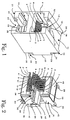
- a most preferred embodiment according to the invention includes eight-pole RJ-45 modular jack connectors which are described in more detail below and with reference to Figs. 1 and 2.
- mateable RJ-45 modular plug connector which associated mateable RJ-45 modular plug connector is well known to a person skilled in the art and, therefore, not shown in the drawings
- the contacts 1, 2, 3, 4, 5, 6, 7, 8 associated with a mateable RJ-45 modular plug connector respectively project laterally, i.e., slightly from above and slightly from below as shown Figure 1, respectively, in front receptacle 9, 10 of dielectric connector housing 11.
- a respective associated eight-pole RJ-45 modular plug connector (not shown in the drawing) is insertable into receptacles 9, 10 from the front side of the modular jack housing 11.
- openings 18, 19 in the upper side wall 16 or lower side wall 17 of dielectric modular jack connector housing 11, permit a modular jack design with particularly low housing height.
- the upper and lower side walls 16, 17 of receptacles 9, 10, respectively, define openings 18, 19 but still provide a secure seating of an inserted associated modular plug connector.
- the locking of the latch element of an inserted, associated modular plug takes place in a reliable manner due to the cooperation with ramp-shaped projections 12, 13, 14, 15 of dielectric housing 11 which project laterally into openings 18, 19.
- openings 18 and 19 on the upper and lower sides extend to a floor or roof wall section 20, 21.
- Two insertion channels 22 and 23, are arranged one above the other and are open to the rear side of dielectric modular jack housing 11; whereby, as is best seen in Figure 4, the longitudinal extension of insertion channels 22 and 23 runs essentially parallel to the insertion direction of the associated modular jack connector.
- modular jack connector housing 11 In the embodiment of modular jack connector housing 11 shown in Figure 1, rectangular-shaped recesses 24, 25, 26 can be seen, respectively recessed toward the center of modular jack connector housing 11 with respect to center rear wall section 27, in order to allow rearward-extending handling members 28, 29, 30 of insertable elements 31 and 32 to stand out freely.
- the modular jack connector housing 11 is designed without recesses 24, 25, 26, and insertable elements 31 are designed without operating members 28, 29, 30, so that the housing depth of modular jack connector housing 11 is reduced.
- FIG. 2 in which two insertable elements 31, 32 are shown in their relative positions to one another. The positions are assumed in the modular jack connector housing 11 after assembly of the insertable elements 31, 32.
- the respective contacts associated with the mateable modular plug connector of the element 31, 1 to 8, and of the element 32, 1' to 8', are arranged adjacent to one another, and respectively extend out of the front side 33 or 34 of the insertable element 31, 32, such that after insertion of the elements 31 and 32 into the channels 22 and 23, respectively, of the modular jack connector housing 11 the respective contacts assume their operating position and are biased in the direction toward the contacts of an inserted associated modular plug connector.
- contacts 1 to 8 and 1' to 8' have, at least in a forward section, when insertable elements 31, 32 are arranged in the insertion channels 22, 23, a slight inclination toward the longitudinal axis X of the modular jack connector housing 11.
- Respectively, ramp-shaped inward-directed, center housing wall sections 35, 36 project over a front section of the contacts such that during the last part of the insertion all of the contacts 1 to 8 and 1' to 8' are slightly bent back in a direction toward the centerline X of the modular jack housing 11 until they experience a predefined bias or prestress in the direction of contacts 37, 38 of the otherwise not further described associated mateable modular modular plug connector.
- Contacts 37, 38 are shown in Figures 4 to 7 for the sake of clarity to obtain a better understanding of the interaction between an associated mateable modular plug and the modular jack.
- the elements 31, 32 may be held captive by a respective rear side locking and holding element 39 as e.g. may be seen from in Figure 2.
- the locking element 39 shown only by way of example for the insertable element 32, has a respective latching projection 40 which extends in a lateral direction on lateral end sides of the holding element 39.
- the wedge-shaped latching projection 41 which is shown only for the operating member 29 in Figure 2 by way of example, is also formed on the operating element 30 and can in this manner reliably prevent a movement of the elements 31, 32 in the longitudinal direction of the insertion channels 22, 23 if the respective holding element 39 is secured to the modular jack housing 11 in a position inhibiting any movement of the insertable elements in a longitudinal direction of insertion channels 22, 34.
- locking element 39 is in a two-row embodiment of the modular jack connector housing 11 with two or more receptacles 9, 10, apt to hold the external terminals a to h of an upper row element 31 or elements 31 in a predefined fixed position.
- the external terminals a to h of an upper row element 31 or elements 31 are embedded in the dielectric material of locking element 39.
- the base surfaces, facing respectively toward the upper and lower outer side of insertable elements 31, 32 having substantially the shape of a rectangular prism preferably include cover plates 42, 43 or cover foils 42, 43, which cover the interior of the dielectric housing 44, 45 of the element 31, 32, as shown in Figure 2..
- acid-free silicon rubber materials are preferably used as permanently elastic dielectric material in the embodiments shown.
- element 32 in Figure 3 is shown in a perspective view obliquely from above, and without the permanently elastic dielectric sealing medium.
- Inductances 46, 47, 48, 49 comprising ferrite ring cores are adjacently arranged in one plane lying within substantially square dielectric housing 45, such that the longitudinal or center axes thereof are respectively aligned mutually parallel but laterally offset from one another.
- Inductances 46, 47, 48, 49 shown in Figure 3 are, according to the design of the electric circuit, respectively, electrically connected to external terminals a to h by means of sections 50, 51 (shown only by way of example), and are connected to contacts 1', 2' by means of sections 52, 53, likewise shown only by way of example. A more detailed electrical connection scheme will be described hereinbelow with reference to Figures 13 to 17.
- contacts 1' to 8' which are arranged parallel to one another and which are similar in their respective shape, are described by way of example with regard to contact 8'.
- Contact 8' which is in its longitudinal extension in the inserted position of element 32 slightly inclined toward center line X of modular jack housing 11, has first, i.e. at its remote end a substantially straight section 8a.
- Section 8a merges into a region 8b' which is in the assembled position of insertable element 32 slightly curved downward toward the interior of receptacle 10. Further from region 8b', contact 8' first defines a small straight piece 8c' and thereafter a further curved section 8d' connecting substantially straight center piece 8e' with section 8c'.
- Substantially straight center piece 8e' also has in the assembled position of insertable element 32 a slight inclination with respect to the center line X of modular jack connector housing 11, so that upon insertion of the associated mateable modular plug connector a resilient elastic contact is established and center piece 8e' moves back generating a predefined bias and a defined electrical contact. Subsequent to center piece 8e', contact 8' has two curved regions 8f' and 8g', which in the mounted state, again lead the laterally outward arched region of the contact back toward the exterior of receptacle 10.
- contacts 4, 5' shown in the cross sectional view of Figure 4 in order to explain, the further course of substantially like-shaped contacts 1' to 8' as well as 1 to 8.
- FIG. 5 shows two elements 31, 32 arranged one behind the other in insertion channel 23.
- the embodiment shown in Figure 5 has, instead of rear s-shaped contact section 5h', 4h, respectively a u-shaped contact section 4i and 5i', which in case of contact section 5i' turns into a bend running sharply to the left directly at dielectric housing 45 of element 32.
- contacts 4 and 5' In order to increase the effective resilient length of contacts 4 and 5', according to Figure 5, they each have a short straight section behind receptacle 9, 10. Behind this short straight section there extends a further straight section 4h, 5h' which preferably is insert molded in dielectrical material and which then emerges from the dielectric material of modular jack connector housing 11 and, in case of contact 4, merges directly into an upward bend, adjoined by a substantially U-shaped section 4i which then leads uninterruptedly into dielectric housing 44 of element 31.
- respective forward contact sections 5a' and 4a arranged in receptacle 9, 10 are kept substantially shorter than in the embodiments shown in Figs 1, 2, 3 and 4.
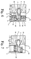
- the embodiment shown in Figure 6 has, in contrast to the embodiment shown in Figure 4, two elements 30, 31 which are pivoted relative on one another for an angle of about 180°. Instead of the contacts which run laterally, this embodiment has contacts which emerge at the respective lateral end from elements 31, 32.
- this embodiment not only the longitudinal axes of the ferrite ring cores are arranged with a mutual lateral offset within the respective elements 31, 32, but also the longitudinal axes of the ferrite ring cores of different elements 31, 32 are arranged laterally offset from one another but remain essentially in the same plane. The coupling by stray magnetic fields is thereby greatly reduced, i.e. is of a very low strength.
- terminals a to i and a' to i' are respectively located in one plane, such that only external terminals d and d' can be seen in the cross sectional view.
- external terminals a to i of element 31, and external terminals a' to i' of element 32 are alternately arranged to be laterally offset to each other and thereby form for each connection element 30, 31 two rows of external terminal elements, whereby the cross-talk between each row of external terminals a to i and a' to i' is reduced.
- Figure 8 may be referred to for a better understanding, by way of example, which figure shows a further embodiment of modular jack connector housing 11 with two rows of receptacles 9, 10 for respective associated RJ-45 mateable modular plug connectors.
- Figure 8 shows the front view of a housing 11 having eight receptacles 9, 10 and
- Figure 9 shows a cross section through modular jack connector housing 11.
- the plane of the cross sectional view of Figure 9 is plane A-A' shown in Figure 8.
- a particularly high packaging density is obtained due to the reduced thickness of partition walls 54 which are respectively arranged between receptacles 9, and the reduced thickness of partition walls 55 which are respectively arranged between receptacles 10.
- the thickness of partition walls 54 and 55 substantially corresponds to, or is even slightly smaller than, the thickness of outer walls 56.
- Contacts 1 to 8 and 1' to 8' are connected to elements 31 and 32 by means of a foil conductor 57.
- terminal wires made of stamped and bent metal extend between elements 31 and 30 and to contacts 1 to 8 and 1' to 8'.
- Figure 10 shows the subassembly for dc separation and for filtering purposes having inductances 47, 48 in the insertable elements 31, 32 and also the connection to the foil conductor or to terminal wires 57 which at the respective end sections are embedded by injection molding within the dielectric housings 44 and 45.
- Figure 11 shows in a lateral cross section view, substantially corresponding to that of Figure 10, the subassembly of elements 31, 32 during their assembly.
- FIG 12 shows elements 30 and 31 as seen in the direction of arrow B of Figure 11.
- Dielectric housings 44, 45 include holding sections 58 and 59 respectively, which are designed as thickened side walls of housing 44, 45.
- contacts 4 and 5' i.e., also contacts 1 to 8 and 1' to 8' which are not shown in detail, are embedded by injection molding in dielectric modular jack connector housing 11, and their free ends 65 to 68 project laterally to the right of the housing.
- connection surfaces 60 to 64 of the foil conductor or of contact wires 57 see Figs. 11 and 12, first come into contact with free ends 65 to 68 which then extend through the connection surfaces and establish electrical contact.
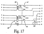
- the electrical circuitry includes inductances 46, 47, 48 and 49 located in elements 31 and 32, respectively.
- Electrical transformers T1 and T2 define a subassembly for dc separation which separation is, in case of a complete galvanic decoupling as shown in Figs. 13, a dc isolation.
- Center taps b and f establish respective midpoint reference potentials, so that the primary sides of isolation transformers T1 and T2 may be respectively driven with symmetrical input signals, which type of signal also is known as "dual rail signal".
- a respective common mode choke coil 47 or 49 is connected to the secondary side (or primary side) of isolation transformers T1 and T2.
- common mode choke coil 47 suppresses in-phase or common mode signal portions at contacts 1 and 2
- common mode choke coil 49 suppresses corresponding signal potions at contact pair 3, 6.
- common mode choke coils 47 and 49 define a filtering device apt to suppress respective undesired signal portions.
- the contacts 4 and 5, which are connected together and which preferably contact an unused conductor pair are connected to resistor R1; and contacts 7 and 8, which are connected together, are connected to resistor R2.
- the second sides of resistors R1 and R2 are connected to the external connection i.
- the unused conductor pair may be grounded by application of a ground potential or suitably chosen direct current reference potential to external connection i.
- any interference signals produced on these lines may be connected to ground there.
- FIG 15 A further alternate embodiment of the electrical circuit arrangement shown in Figure 14 is shown in Figure 15. It further includes resistors R3 and R4 in the secondary side connection lead to the respective center taps of isolation transformers T1 or T2, by which means the center taps of isolation transformers T1 or T2 are grounded.
- a suitable impedance for transmission may be provided at contact pair 1, 2 or 3, 6 by means of the respective resistors R3 and R4.
- a direct current (dc) decoupled and potential-free connection arrangement is provided with respect to contacts 1 to 8; however, for higher frequencies, a common reference potential may be provided hereby for the unused conductor pair 4, 5 and a midpoint potential of the signals may be established at contact pairs 1, 2 and 3, 6.
Applications Claiming Priority (2)
| Application Number | Priority Date | Filing Date | Title |
|---|---|---|---|
| DE29819314U DE29819314U1 (de) | 1998-10-29 | 1998-10-29 | Buchsenartiger Steckverbinder mit Filtereinrichtung |
| DE29819314U | 1998-10-29 |
Publications (3)
| Publication Number | Publication Date |
|---|---|
| EP0997989A2 true EP0997989A2 (de) | 2000-05-03 |
| EP0997989A3 EP0997989A3 (de) | 2002-02-06 |
| EP0997989B1 EP0997989B1 (de) | 2006-06-07 |
Family
ID=8064579
Family Applications (1)
| Application Number | Title | Priority Date | Filing Date |
|---|---|---|---|
| EP99121444A Expired - Lifetime EP0997989B1 (de) | 1998-10-29 | 1999-10-28 | Modularer Steckverbinder mit einer Gleichstrom-Entkopplungsschaltung und Filter |
Country Status (7)
| Country | Link |
|---|---|
| US (1) | US6302741B1 (de) |
| EP (1) | EP0997989B1 (de) |
| JP (1) | JP3446135B2 (de) |
| KR (1) | KR100316494B1 (de) |
| CN (1) | CN1108651C (de) |
| DE (2) | DE29819314U1 (de) |
| TW (1) | TW433615U (de) |
Cited By (3)
| Publication number | Priority date | Publication date | Assignee | Title |
|---|---|---|---|---|
| GB2366081A (en) * | 2000-08-09 | 2002-02-27 | Motorola Israel Ltd | Radiation-efficient portable radio antenna which adapts to conditions |
| EP1182746A1 (de) * | 2000-08-23 | 2002-02-27 | F.C.I. - Framatome Connectors International | Elektrischer Anreihverbinder zur Verwendung mit einem Filter |
| EP1306934A1 (de) * | 2001-10-29 | 2003-05-02 | Setec Netzwerke AG | Buchse und Anschlussdose zur Herstellung einer Hochleistungs-Datenleitungsverbindung |
Families Citing this family (36)
| Publication number | Priority date | Publication date | Assignee | Title |
|---|---|---|---|---|
| US20020119702A1 (en) * | 2000-08-22 | 2002-08-29 | John Chen | EMI suppression technique for RJ connectors with integrated magnetics |
| US6585540B2 (en) * | 2000-12-06 | 2003-07-01 | Pulse Engineering | Shielded microelectronic connector assembly and method of manufacturing |
| DE10120362A1 (de) * | 2001-04-26 | 2002-11-21 | Integrated Electronic Systems Sys Consulting Gmbh | Spritzgussformteil |
| US6663437B2 (en) * | 2001-11-08 | 2003-12-16 | Hon Hai Precision Ind. Co., Ltd. | Stacked modular jack assembly having built-in circuit boards |
| US6568966B1 (en) * | 2001-11-08 | 2003-05-27 | Hon Hai Precision Ind. Co., Ltd. | Stacked modular jack assembly having improved magnetic module |
| US6623307B2 (en) * | 2001-11-08 | 2003-09-23 | Hon Hai Precision Ind. Co., Ltd. | High frequency modular jack connector |
| US6537110B1 (en) * | 2001-11-08 | 2003-03-25 | Hon Hai Precision Ind. Co., Ltd. | Stacked modular jack assembly having highly modularized electronic components |
| US20030157843A1 (en) * | 2002-02-15 | 2003-08-21 | Keith Thomas | Stacking connector with improper plug type prevention |
| DE20205701U1 (de) * | 2002-04-12 | 2003-05-28 | Siemens Ag | Variable Feldbusankopplung mit großer Kopplungslänge, insbesondere für mobile Bedien- und Beobachtungsgeräte |
| TW579102U (en) * | 2002-06-28 | 2004-03-01 | Hon Hai Prec Ind Co Ltd | Module connector |
| US6641440B1 (en) * | 2002-09-30 | 2003-11-04 | Hon Hai Precision Ind. Co., Ltd. | Electrical connector with power module |
| US6743047B2 (en) | 2002-10-23 | 2004-06-01 | Hon Hai Precision Ind. Co., Ltd. | Electrical connector with rear ground plate |
| US6752664B2 (en) * | 2002-10-24 | 2004-06-22 | Hon Hai Precision Ind. Co., Ltd. | Modular jack having magnetic module with support and alignment mechanism |
| JP3800536B2 (ja) * | 2002-12-06 | 2006-07-26 | Tdk株式会社 | モジュラジャック |
| US6848947B2 (en) * | 2003-05-23 | 2005-02-01 | William J. Chimiak | Cross-connector for interfacing multiple communication devices |
| US6776651B1 (en) * | 2003-06-20 | 2004-08-17 | Lankom Electronics Co., Ltd. | Stacked electronic connector |
| TWM249341U (en) * | 2003-09-19 | 2004-11-01 | Hon Hai Prec Ind Co Ltd | Modular jack |
| US20060246784A1 (en) * | 2005-04-29 | 2006-11-02 | Aekins Robert A | Electrically isolated shielded connector system |
| US7134915B1 (en) * | 2005-12-16 | 2006-11-14 | Superworld Electronics Co., Ltd. | Base structure for communication module |
| US7377819B1 (en) * | 2006-04-27 | 2008-05-27 | Arrowhead Center, Inc. | Method and apparatus for improving network connection security with one or more cross-wired adapters |
| US7530854B2 (en) * | 2006-06-15 | 2009-05-12 | Ortronics, Inc. | Low noise multiport connector |
| DE102006036459B3 (de) | 2006-08-04 | 2007-12-27 | Adc Gmbh | Steckverbinder für die Telekommunikations- und Datentechnik |
| US7429178B2 (en) * | 2006-09-12 | 2008-09-30 | Samtec, Inc. | Modular jack with removable contact array |
| US7288001B1 (en) | 2006-09-20 | 2007-10-30 | Ortronics, Inc. | Electrically isolated shielded multiport connector assembly |
| US7708602B2 (en) * | 2007-03-01 | 2010-05-04 | Pulse Engineering, Inc. | Connector keep-out apparatus and methods |
| US7863776B2 (en) * | 2007-04-04 | 2011-01-04 | Finisar Corporation | Transceiver connector with integrated magnetics |
| CN101662108B (zh) * | 2008-08-27 | 2013-03-13 | 富士康(昆山)电脑接插件有限公司 | 电连接器 |
| US9153897B2 (en) | 2009-11-06 | 2015-10-06 | Molex, Llc | Mag-jack module |
| WO2011056968A2 (en) * | 2009-11-06 | 2011-05-12 | Molex Incorporated | Circuit member with enhanced performance |
| CN103022818B (zh) | 2011-09-28 | 2015-04-01 | 富士康(昆山)电脑接插件有限公司 | 电连接器 |
| KR101425730B1 (ko) | 2012-11-21 | 2014-08-01 | 아이메트 인더스트리얼 컴퍼니 리미티드 | 커넥터 구조 |
| US9419391B2 (en) | 2013-08-20 | 2016-08-16 | Panduit Corp. | Communication connector |
| CN104810684B (zh) * | 2014-01-23 | 2017-03-08 | 富誉电子科技(淮安)有限公司 | 电连接器 |
| DE102014109867A1 (de) * | 2014-07-14 | 2016-01-14 | Erni Production Gmbh & Co. Kg | Steckverbinder und Bauelement |
| US9525242B1 (en) | 2015-08-24 | 2016-12-20 | Cisco Technology, Inc. | Modular connectors with electromagnetic interference suppression |
| US9907159B2 (en) * | 2016-07-12 | 2018-02-27 | Fluke Corporation | Plug connector for tuning crosstalk and return loss |
Citations (5)
| Publication number | Priority date | Publication date | Assignee | Title |
|---|---|---|---|---|
| US5282759A (en) * | 1991-09-13 | 1994-02-01 | Murata Manufacturing Co., Ltd. | Modular jack |
| EP0658953A2 (de) * | 1993-12-14 | 1995-06-21 | The Whitaker Corporation | Anordnung von modularen Steckern mit einer Mehrzahl von Öffnungen |
| US5647767A (en) * | 1995-02-06 | 1997-07-15 | The Whitaker Corporation | Electrical connector jack assembly for signal transmission |
| US5687233A (en) * | 1996-02-09 | 1997-11-11 | Maxconn Incorporated | Modular jack having built-in circuitry |
| WO1997047083A1 (en) * | 1996-06-03 | 1997-12-11 | Amphenol Corporation | Common mode filter and filter/connector combination |
Family Cites Families (9)
| Publication number | Priority date | Publication date | Assignee | Title |
|---|---|---|---|---|
| US4772224A (en) | 1987-09-02 | 1988-09-20 | Corcom, Inc. | Modular electrical connector |
| JPH07120542B2 (ja) | 1988-12-12 | 1995-12-20 | 株式会社村田製作所 | モジュラージャック |
| US5069641A (en) | 1990-02-03 | 1991-12-03 | Murata Manufacturing Co., Ltd. | Modular jack |
| US5139442A (en) | 1990-12-03 | 1992-08-18 | Murata Manufacturing Co., Ltd. | Modular jack |
| US5587884A (en) | 1995-02-06 | 1996-12-24 | The Whitaker Corporation | Electrical connector jack with encapsulated signal conditioning components |
| GB9523588D0 (en) | 1995-11-17 | 1996-01-17 | Amp Holland | Modular jack having reduced cross-talk enhancement |
| US5816830A (en) * | 1995-12-15 | 1998-10-06 | The Whitaker Corporation | Electrical connector module for a high density electrical connector |
| US5971805A (en) | 1997-05-27 | 1999-10-26 | Berg Technology, Inc. | Modular jack with filter insert |
| US6019631A (en) * | 1999-08-09 | 2000-02-01 | Hon Hai Precision Ind. Co., Ltd. | Stacked electrical connector assembly |
-
1998
- 1998-10-29 DE DE29819314U patent/DE29819314U1/de not_active Expired - Lifetime
-
1999
- 1999-10-18 JP JP33172699A patent/JP3446135B2/ja not_active Expired - Fee Related
- 1999-10-19 US US09/420,884 patent/US6302741B1/en not_active Expired - Fee Related
- 1999-10-25 TW TW088218086U patent/TW433615U/zh not_active IP Right Cessation
- 1999-10-28 EP EP99121444A patent/EP0997989B1/de not_active Expired - Lifetime
- 1999-10-28 CN CN99127354A patent/CN1108651C/zh not_active Expired - Fee Related
- 1999-10-28 DE DE69931726T patent/DE69931726T2/de not_active Expired - Lifetime
- 1999-10-28 KR KR1019990047014A patent/KR100316494B1/ko not_active IP Right Cessation
Patent Citations (5)
| Publication number | Priority date | Publication date | Assignee | Title |
|---|---|---|---|---|
| US5282759A (en) * | 1991-09-13 | 1994-02-01 | Murata Manufacturing Co., Ltd. | Modular jack |
| EP0658953A2 (de) * | 1993-12-14 | 1995-06-21 | The Whitaker Corporation | Anordnung von modularen Steckern mit einer Mehrzahl von Öffnungen |
| US5647767A (en) * | 1995-02-06 | 1997-07-15 | The Whitaker Corporation | Electrical connector jack assembly for signal transmission |
| US5687233A (en) * | 1996-02-09 | 1997-11-11 | Maxconn Incorporated | Modular jack having built-in circuitry |
| WO1997047083A1 (en) * | 1996-06-03 | 1997-12-11 | Amphenol Corporation | Common mode filter and filter/connector combination |
Cited By (6)
| Publication number | Priority date | Publication date | Assignee | Title |
|---|---|---|---|---|
| GB2366081A (en) * | 2000-08-09 | 2002-02-27 | Motorola Israel Ltd | Radiation-efficient portable radio antenna which adapts to conditions |
| EP1182746A1 (de) * | 2000-08-23 | 2002-02-27 | F.C.I. - Framatome Connectors International | Elektrischer Anreihverbinder zur Verwendung mit einem Filter |
| JP2002093530A (ja) * | 2000-08-23 | 2002-03-29 | Fci | フイルタ挿入物と共に使用するための積み重ね式電気コネクタ |
| EP1306934A1 (de) * | 2001-10-29 | 2003-05-02 | Setec Netzwerke AG | Buchse und Anschlussdose zur Herstellung einer Hochleistungs-Datenleitungsverbindung |
| WO2003038951A1 (de) * | 2001-10-29 | 2003-05-08 | Setec Netzwerke Ag | Buchse und anschlussdose zur herstellung einer hochleistungs-datenleitungsverbindung |
| US6840779B2 (en) | 2001-10-29 | 2005-01-11 | Setec Netzwerke Ag | High power data line connection |
Also Published As
| Publication number | Publication date |
|---|---|
| KR100316494B1 (ko) | 2001-12-12 |
| CN1108651C (zh) | 2003-05-14 |
| DE29819314U1 (de) | 2000-03-02 |
| EP0997989B1 (de) | 2006-06-07 |
| JP2001060480A (ja) | 2001-03-06 |
| DE69931726T2 (de) | 2007-06-14 |
| DE69931726D1 (de) | 2006-07-20 |
| KR20000035088A (ko) | 2000-06-26 |
| JP3446135B2 (ja) | 2003-09-16 |
| EP0997989A3 (de) | 2002-02-06 |
| US6302741B1 (en) | 2001-10-16 |
| TW433615U (en) | 2001-05-01 |
| CN1258116A (zh) | 2000-06-28 |
Similar Documents
| Publication | Publication Date | Title |
|---|---|---|
| US6302741B1 (en) | Modular connector with DC decoupling and filtering | |
| US8992248B2 (en) | Modular jack with enhanced port isolation | |
| CA2085270C (en) | High frequency electrical connector | |
| US5647767A (en) | Electrical connector jack assembly for signal transmission | |
| US8888538B2 (en) | Modular jack with enhanced shielding | |
| US6068520A (en) | Low profile double deck connector with improved cross talk isolation | |
| US7048550B2 (en) | Electrical adapter assembly | |
| US6419526B1 (en) | High frequency bi-level offset multi-port jack | |
| US7153163B2 (en) | Modular jack for ethernet applications | |
| US8449332B2 (en) | Filtering assembly and modular jack using same | |
| EP0986839B1 (de) | Modularstecker mit eingebautem elektronischen komponent | |
| US5872492A (en) | Circuit boardless common mode filter and transformer connector | |
| US20110053418A1 (en) | Modular jack with two-piece housing and insert | |
| US10418756B2 (en) | Plug connector with integrated galvanic separation and shielding element | |
| US6783398B2 (en) | Shielded modular jack assembly for ethernet applications | |
| US6736680B2 (en) | Modular jack assembly for ethernet applications | |
| US20030087555A1 (en) | Modular jack assembly having improved positioning means | |
| WO1996024968A1 (en) | Electrical connector jack assembly for signal transmission | |
| CN112615212A (zh) | 具有安全连接器和磁性元件的网络插座 | |
| JP2001148270A (ja) | 内部シールドを有する電気コネクタ |
Legal Events
| Date | Code | Title | Description |
|---|---|---|---|
| PUAI | Public reference made under article 153(3) epc to a published international application that has entered the european phase |
Free format text: ORIGINAL CODE: 0009012 |
|
| AK | Designated contracting states |
Kind code of ref document: A2 Designated state(s): AT BE CH CY DE DK ES FI FR GB GR IE IT LI LU MC NL PT SE Kind code of ref document: A2 Designated state(s): DE FR GB |
|
| AX | Request for extension of the european patent |
Free format text: AL;LT;LV;MK;RO;SI |
|
| PUAL | Search report despatched |
Free format text: ORIGINAL CODE: 0009013 |
|
| AK | Designated contracting states |
Kind code of ref document: A3 Designated state(s): AT BE CH CY DE DK ES FI FR GB GR IE IT LI LU MC NL PT SE |
|
| AX | Request for extension of the european patent |
Free format text: AL;LT;LV;MK;RO;SI |
|
| 17P | Request for examination filed |
Effective date: 20020713 |
|
| AKX | Designation fees paid |
Free format text: DE FR GB |
|
| 17Q | First examination report despatched |
Effective date: 20040525 |
|
| GRAP | Despatch of communication of intention to grant a patent |
Free format text: ORIGINAL CODE: EPIDOSNIGR1 |
|
| GRAS | Grant fee paid |
Free format text: ORIGINAL CODE: EPIDOSNIGR3 |
|
| GRAA | (expected) grant |
Free format text: ORIGINAL CODE: 0009210 |
|
| AK | Designated contracting states |
Kind code of ref document: B1 Designated state(s): DE FR GB |
|
| REG | Reference to a national code |
Ref country code: GB Ref legal event code: FG4D |
|
| REF | Corresponds to: |
Ref document number: 69931726 Country of ref document: DE Date of ref document: 20060720 Kind code of ref document: P |
|
| ET | Fr: translation filed | ||
| PLBE | No opposition filed within time limit |
Free format text: ORIGINAL CODE: 0009261 |
|
| STAA | Information on the status of an ep patent application or granted ep patent |
Free format text: STATUS: NO OPPOSITION FILED WITHIN TIME LIMIT |
|
| 26N | No opposition filed |
Effective date: 20070308 |
|
| PGFP | Annual fee paid to national office [announced via postgrant information from national office to epo] |
Ref country code: FR Payment date: 20081018 Year of fee payment: 10 |
|
| PGFP | Annual fee paid to national office [announced via postgrant information from national office to epo] |
Ref country code: GB Payment date: 20081029 Year of fee payment: 10 |
|
| REG | Reference to a national code |
Ref country code: FR Ref legal event code: ST Effective date: 20100630 |
|
| PG25 | Lapsed in a contracting state [announced via postgrant information from national office to epo] |
Ref country code: FR Free format text: LAPSE BECAUSE OF NON-PAYMENT OF DUE FEES Effective date: 20091102 |
|
| PG25 | Lapsed in a contracting state [announced via postgrant information from national office to epo] |
Ref country code: GB Free format text: LAPSE BECAUSE OF NON-PAYMENT OF DUE FEES Effective date: 20091028 |
|
| PGFP | Annual fee paid to national office [announced via postgrant information from national office to epo] |
Ref country code: DE Payment date: 20101027 Year of fee payment: 12 |
|
| PG25 | Lapsed in a contracting state [announced via postgrant information from national office to epo] |
Ref country code: DE Free format text: LAPSE BECAUSE OF NON-PAYMENT OF DUE FEES Effective date: 20120501 |
|
| REG | Reference to a national code |
Ref country code: DE Ref legal event code: R119 Ref document number: 69931726 Country of ref document: DE Effective date: 20120501 |