EP0996026A2 - Reflection type liquid crystal display - Google Patents
Reflection type liquid crystal display Download PDFInfo
- Publication number
- EP0996026A2 EP0996026A2 EP99308283A EP99308283A EP0996026A2 EP 0996026 A2 EP0996026 A2 EP 0996026A2 EP 99308283 A EP99308283 A EP 99308283A EP 99308283 A EP99308283 A EP 99308283A EP 0996026 A2 EP0996026 A2 EP 0996026A2
- Authority
- EP
- European Patent Office
- Prior art keywords
- liquid crystal
- substrate
- reflective display
- insulating film
- reflection type
- Prior art date
- Legal status (The legal status is an assumption and is not a legal conclusion. Google has not performed a legal analysis and makes no representation as to the accuracy of the status listed.)
- Withdrawn
Links
Images


Classifications
-
- G—PHYSICS
- G02—OPTICS
- G02F—OPTICAL DEVICES OR ARRANGEMENTS FOR THE CONTROL OF LIGHT BY MODIFICATION OF THE OPTICAL PROPERTIES OF THE MEDIA OF THE ELEMENTS INVOLVED THEREIN; NON-LINEAR OPTICS; FREQUENCY-CHANGING OF LIGHT; OPTICAL LOGIC ELEMENTS; OPTICAL ANALOGUE/DIGITAL CONVERTERS
- G02F1/00—Devices or arrangements for the control of the intensity, colour, phase, polarisation or direction of light arriving from an independent light source, e.g. switching, gating or modulating; Non-linear optics
- G02F1/01—Devices or arrangements for the control of the intensity, colour, phase, polarisation or direction of light arriving from an independent light source, e.g. switching, gating or modulating; Non-linear optics for the control of the intensity, phase, polarisation or colour
- G02F1/13—Devices or arrangements for the control of the intensity, colour, phase, polarisation or direction of light arriving from an independent light source, e.g. switching, gating or modulating; Non-linear optics for the control of the intensity, phase, polarisation or colour based on liquid crystals, e.g. single liquid crystal display cells
- G02F1/133—Constructional arrangements; Operation of liquid crystal cells; Circuit arrangements
- G02F1/1333—Constructional arrangements; Manufacturing methods
- G02F1/1343—Electrodes
-
- G—PHYSICS
- G02—OPTICS
- G02F—OPTICAL DEVICES OR ARRANGEMENTS FOR THE CONTROL OF LIGHT BY MODIFICATION OF THE OPTICAL PROPERTIES OF THE MEDIA OF THE ELEMENTS INVOLVED THEREIN; NON-LINEAR OPTICS; FREQUENCY-CHANGING OF LIGHT; OPTICAL LOGIC ELEMENTS; OPTICAL ANALOGUE/DIGITAL CONVERTERS
- G02F1/00—Devices or arrangements for the control of the intensity, colour, phase, polarisation or direction of light arriving from an independent light source, e.g. switching, gating or modulating; Non-linear optics
- G02F1/01—Devices or arrangements for the control of the intensity, colour, phase, polarisation or direction of light arriving from an independent light source, e.g. switching, gating or modulating; Non-linear optics for the control of the intensity, phase, polarisation or colour
- G02F1/13—Devices or arrangements for the control of the intensity, colour, phase, polarisation or direction of light arriving from an independent light source, e.g. switching, gating or modulating; Non-linear optics for the control of the intensity, phase, polarisation or colour based on liquid crystals, e.g. single liquid crystal display cells
- G02F1/133—Constructional arrangements; Operation of liquid crystal cells; Circuit arrangements
- G02F1/1333—Constructional arrangements; Manufacturing methods
- G02F1/1335—Structural association of cells with optical devices, e.g. polarisers or reflectors
- G02F1/133553—Reflecting elements
-
- G—PHYSICS
- G02—OPTICS
- G02F—OPTICAL DEVICES OR ARRANGEMENTS FOR THE CONTROL OF LIGHT BY MODIFICATION OF THE OPTICAL PROPERTIES OF THE MEDIA OF THE ELEMENTS INVOLVED THEREIN; NON-LINEAR OPTICS; FREQUENCY-CHANGING OF LIGHT; OPTICAL LOGIC ELEMENTS; OPTICAL ANALOGUE/DIGITAL CONVERTERS
- G02F1/00—Devices or arrangements for the control of the intensity, colour, phase, polarisation or direction of light arriving from an independent light source, e.g. switching, gating or modulating; Non-linear optics
- G02F1/01—Devices or arrangements for the control of the intensity, colour, phase, polarisation or direction of light arriving from an independent light source, e.g. switching, gating or modulating; Non-linear optics for the control of the intensity, phase, polarisation or colour
- G02F1/13—Devices or arrangements for the control of the intensity, colour, phase, polarisation or direction of light arriving from an independent light source, e.g. switching, gating or modulating; Non-linear optics for the control of the intensity, phase, polarisation or colour based on liquid crystals, e.g. single liquid crystal display cells
- G02F1/133—Constructional arrangements; Operation of liquid crystal cells; Circuit arrangements
- G02F1/1333—Constructional arrangements; Manufacturing methods
- G02F1/1335—Structural association of cells with optical devices, e.g. polarisers or reflectors
- G02F1/133504—Diffusing, scattering, diffracting elements
Definitions
- the present invention relates to a reflection type liquid crystal display.
- Fig. 1 is a sectional view of one such conventional reflection type liquid crystal display.
- such a conventional reflection type liquid crystal display has a thin film transistor (hereinafter referred to as the TFT) as a switching element on an insulating substrate 10 of quartz glass or non-alkali glass or the like.
- the TFT thin film transistor
- gate electrodes 11 of a refractory metal such as chromium (Cr) or molybdenum (Mo)
- a gate insulating film 12 and active layers 13 of polysilicon films are successively formed on the insulating substrate (TFT substrate) 10.
- Each active layer 13 includes channels 13c formed above the gate electrodes 11, and a source 13s and a drain 13d that are formed on both sides of the channels 13c by ion doping using stopper insulating films 14 on the channels 13c as masks.
- an inter-layer insulating film 15 which includes a SiO 2 film, a SiN film and a SiO 2 film deposited in succession, is formed over the entire surfaces of the gate insulating film 12, the active layer 13 and the stopper insulating films 14.
- a drain electrode 16 is formed by filling a contact hole, which is formed to correspond to the drain 13d, with a metal, such as aluminum (Al).
- a contact hole is formed at a location of the planarization insulating film 17 corresponding to the source 13s.
- An alignment film 20 consisting of an organic resin, such as polyimide, and aligning liquid crystal elements 21, is formed on the reflective display electrode 19.
- a color filter 31 including primary colors, red (R), green (G), and blue (B) and a black matrix 32 with a function to shield light; a protective film 33 of a resin formed on the color filter 31; and a counter electrode 34 and an alignment film 35 formed over the entire surface of the protective film 33.
- a polarizer 41 is located on the side not facing the TFT substrate 10. The counter electrode substrate 30 and the TFT substrate 10 are bonded together with their peripheries sealed with a sealing bond (not shown), thus forming a space inside, and this space is filled with a twisted nematic (TN) liquid crystal 21.
- TN twisted nematic
- a natural light 100 coming from the outside enters from the polarizer 41 on the side of an observer 101, and passes through the counter electrode substrate 30, the color filter 31, the protective film 33, the counter electrode 34, the alignment film 35, the alignment film 20, the TN liquid crystal 21, and the alignment film 20 on the TFT substrate 10.
- the light is reflected by the reflective display electrode 19, travels through the layers in a direction opposite to the direction of incidence, emerges from the polarizer 41 on the counter electrode substrate 30 and enters the eyes of the observer 101.
- the observed display in a specific viewing angle can be bright by the light having passed through a place other than the place not related with the display, but the entire observed image is disadvantageously dark.
- an image blur, or a bleeding of a color image tends to be easily generated because the light of a pixel to be displayed is emitted from other pixels in the vicinity as shown in Fig. 1.
- the present invention has been made to rectify the disadvantages described above and has as its object to provide a reflection type liquid crystal display that enhances a luminance of each display pixel and offers a high-quality display.
- a reflection type liquid crystal display which comprises a liquid crystal held in a gap between a first substrate and a second substrate disposed facing each other, and electrodes for driving the liquid crystal for each pixel disposed on the first and second substrates facing the liquid crystal.
- the electrode on the first substrate comprises a plurality of reflective display electrodes divided for the pixels and formed of conductive reflective materials, and each of the plurality of reflective display electrodes has a concavity toward the first substrate on at least a surface facing the liquid crystal.
- a switching element for each pixel is further formed on the first substrate, and the switching element is connected to the corresponding electrode out of the plurality of reflective display electrodes.
- At least a surface of the reflective display electrode facing the liquid crystal is concaved toward the first substrate in the vicinity of a pixel area center.
- the reflective display electrode is provided with the concavity in each pixel area, the light reflected by the reflective display electrode is converged within the pixel area, so that the light is prevented from being propagated or lost through a light shield area other than the pixel area as an invalid light, or from being emitted from an adjacent pixel area. Therefore, the luminance of the reflected light obtained in each display pixel can substantially be enhanced. Moreover, since the reflected light is emitted from the same pixel area without leaking to adjacent pixels, image blur and the bleeding of a displayed color image can be prevented, so that a display quality can be enhanced.
- the second substrate is provided with a light diffusing member, so that the light converged by the concavity of the reflective display electrode can be diffused and emitted. Therefore, the intensity of the emitted light can be uniformed in a single pixel, luminance nonuniformity is prevented and the display quality can further be enhanced.
- the concavity of the reflective display electrode may also be obtained by the following constitution.
- At least an insulating film is formed between the reflective display electrode and the first substrate.
- a concavity toward the first substrate is formed on the surface of the insulating film facing the liquid crystal for each of the pixel areas.
- the concavity of the insulating film is continued to the surface of the reflective display electrode facing the liquid crystal, formed on the insulating film.
- the switching element formed for each pixel and a wire for supplying a signal to the switching element are formed on the first substrate.
- the plurality of reflective display electrodes are formed on the insulating film which is formed on the whole surface of the substrate so as to cover the switching element and the wire.
- Each of the plurality of reflective display electrodes is positioned so as to cover rising areas disposed by the provision of the corresponding switching element and/or the wire on the surface of the insulating film and a concaved area held between the rising areas, and irregularities of the surface of the insulating film are continued to the surface of the reflective display electrode facing the liquid crystal.
- a reflection type liquid crystal display which comprises a liquid crystal held in a gap between a first substrate and a second substrate disposed facing each other; and electrodes for driving the liquid crystal disposed on the first and second substrates facing the liquid crystal.
- the electrode formed on one of the first and second substrates is a reflective display electrode formed of a conductive reflective material, and at least a surface of the reflective display electrode facing the liquid crystal has a concavity toward the substrate in each pixel area.
- a method of manufacturing a reflection type liquid crystal display provided with a liquid crystal held in a gap between a first substrate and a second substrate disposed facing each other, and electrodes for driving the liquid crystal formed on the first and second substrates facing the liquid crystal, said method comprising the steps of forming a reflective display electrode with a conductive reflective material on the first substrate and of selectively etching the surface of the reflective display electrode to form a concavity toward the first substrate on the surface of the reflective display electrode.
- a method of manufacturing a reflection type liquid crystal display provided with a liquid crystal held in a gap between a first substrate and a second substrate disposed facing each other, and electrodes for driving the liquid crystal formed on the first and second substrates facing the liquid crystal, said method comprising the steps of forming an insulating film on the first substrate; selectively etching the surface of the insulating film to form a concavity toward the first substrate for each pixel area on the surface of the insulating film; and forming a reflective display electrode with a conductive reflective material on the insulating film.
- a reflection type liquid crystal display can be obtained, in which the luminance of each display pixel is enhanced, and a bright image can be displayed in a wider viewing angle.
- the reflection type liquid crystal display according to the present invention will be described in the following.
- Fig. 2 is a sectional view of a first embodiment of the present invention.
- TFT as a switching element is formed on an insulating substrate 10 of quartz glass or non-alkali glass or the like.
- the structure from the gate electrode 11 of a refractory metal, such as Cr and Mo, up to the planarization insulating film 17 on the insulating substrate 10, is formed as in conventional display units, the description of those components is omitted.
- Reflective display electrodes 50 formed of conductive reflective materials, such as Al and silver (Ag) and connected to the sources 13s of the active layer 13 of a polysilicon film, are formed on the planarization insulating film 17.
- a substantially central portion of the display electrode has a concave surface curved toward the TFT substrate 10, that is, substantially the central portion of the display electrode has a curved surface being concave in a direction of TFT substrate 10, and further in other words, the substantially central portion of the display electrode is configured to be depressed toward the TFT substrate.
- the alignment film 20 of polyimide or the like for aligning the liquid crystal is formed on the entire surface covering the reflective display electrodes 50. In this connection, the surface of the display electrode above a contact hole is partially covered is more concaved than the other region surface of the display electrode owing to the influence of the presence of the hole.
- the counter electrode substrate 30 is, on the side facing the liquid crystal 21, provided with a color filter 31 comprising the primary colors R, G and B and a black matrix with a light shielding function, and a protective film 33 formed of an acrylic resin, for example, to protect the color filter 31.
- a counter electrode 34 facing the reflective display electrodes 50 is disposed on the whole surface of the protective film 33.
- an alignment film 35 of polyimide is formed over the entire surface of the counter electrode 34.
- a diffusing layer 43 to diffuse light, a phase ( ⁇ /4) plate 44 and a polarizer 45 are formed in succession.
- TN liquid crystal can, for example, be used.
- Fig. 2 The path traveled by light viewed by a user of the above reflection type liquid crystal display is described in the following.
- the path of incident light is shown in R pixels of the color filter 31
- the path of the incident light and a part of reflected light is shown in G pixels
- the path of the reflected light is shown in B pixels.
- light 100 is incident on each color as shown by each solid line, and the light reflected by the reflective display electrode 50 advances and emerges as shown by the broken line.
- the light reflected in the vicinity of the peripheral edge of the reflective display electrode 50 travels linearly and in parallel, and passes through each color (R, G, B) of the color filter corresponding to the reflective display electrode 50, without passing through a portion not related with display, such as the black matrix.
- the reflected light is diffused by the diffusing layer 43, passes through the phase plate 43 and the polarizer 45, and is viewed by the observer 101.
- the concaved portion formed on the surface of the reflective display electrode 50 owing to the contact hole as described above also plays a partial role of the function for converging the reflected light in the range in which the reflective display electrode 50 is formed.
- the light reflected by the reflective display electrode 50 passes through the liquid crystal 21, the alignment film 35, the counter electrode 34, the protective film 33, the color filter 31, and the counter electrode substrate 30, and is diffused by the diffusing layer 43.
- the light further passes through the phase plate 44 and the polarizer 45 and enters the eyes of the observer 101.
- the diffusing layer 43 is provided, converged light reaching the diffusing layer 43 is diffused in every direction by the diffusing layer 43 and emerges from the phase plate 44 and the polarizer 45. Because of the converging function of the reflective display electrode 50, even when the reflected light from the reflective display electrode 50 fails to reach, for example, the black matrix positioned in the peripheral edge of the pixel, the vicinity of the peripheral edge of the pixel area is prevented from looking dark, so that a bright image can be displayed uniformly over the whole surface.
- Fig. 3A shows a method of measuring the luminance of the surface of the reflection type liquid crystal display
- Fig. 3B is a graph showing measurement results.
- a display side (the side of the counter electrode substrate 30) facing upward in a reflection type liquid crystal display panel provided with the TFT substrate 10 and the counter electrode substrate 30.
- light is allowed to be incident upon the display panel from a direction inclined by a certain angle, for example, ⁇ to a vertical direction to the display surface.
- An incident light 105 is reflected by the reflective display electrode, and an emerging reflected light in each angle is measured by a light intensity detector 106.
- the light intensity detector 106 is moved in an arrow direction from a normal line direction (shown by a broken line in Fig. 3A) of the liquid crystal display panel of Fig. 3A, the angle from the normal line direction is changed, and the reflected light in each angle is detected and measured.
- Fig. 3B The measurement results are shown in Fig. 3B.
- the axis of abscissa shows the detected angle
- the axis of ordinate shows the reflected light intensity in each detected angle.
- a solid curve shows a reflection type liquid crystal display of the present invention
- a broken curve shows a conventional reflection type liquid crystal display.
- angle ⁇ has an opposite direction from the normal line to the incident angle ⁇ of the incident light 105 in Fig. 3A, and has a size equal to that of the incident angle ⁇ .
- the reflex light intensity is strong in a specific angle, that is, the incident angle of the incident light, but according to the reflection type liquid crystal display of the present invention, the reflected light emerges out of the display panel in a wide angle of view, so that bright display can be viewed in a wide range of the display panel.
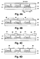
- Figs. 4A to 4D are manufacture process sectional views of the reflection type liquid crystal display of the present invention.
- the planarization insulating film 17, for example, formed of an organic resin is formed on the entire surface to flatten the surface. Subsequently, a contact hole is formed in a position corresponding to the source 13s of the planarization insulating film 17, and the reflective display electrode 50, which consists of Al in contact with the source 13s through this contact hole and serves also as the source electrode, is formed on the planarization insulating film 17.
- a conductive reflective material of Al or Ag or the like which is the material of the reflective display electrode, is first deposited (Fig. 4A).
- Resist patterns 60 are formed in areas, in which the reflective display electrodes 50 are to be formed and a resist remains (Fig. 4B).
- the resist patterns 60 are removed.
- the areas other than the reflective display electrodes 50 are covered with resist patterns 61 (Fig. 4C).
- anisotropic etching is performed by wet etching, the resist patters 61 are removed. In this manner the surface of the reflective display electrode 50 can be provided with a concave curved surface (Fig. 4D).
- an alignment film is formed on the surface to form the TFT substrate 10.
- the resist patterns formed on the reflective display electrodes 50 patterns in which only the substantially central portions of the reflective display electrodes are opened are first formed, and Al is etched. Subsequently, the resist patterns are removed to form new resist patterns having slightly larger openings, and Al is etched. By etching reflective display electrode surfaces in a stepwise manner, the curved surfaces may be formed.
- the reflective display electrode surfaces may substantially be provided with curved surfaces.
- the planarization insulating film 17 is applied to the entire surface, for example, by a spinner. Then, the planarization insulating film 17 can be applied to both surfaces of an area A formed by the drain electrodes 16, the gate electrodes 11, and the like, and protruded from a TFT substrate surface, and a substantially flat area B in which the reflective display electrodes are to be formed. Therefore, the surface of the planarization insulating film 17 itself can be formed into a curved surface which is concaved toward the TFT substrate 10 without especially etching the planarization insulating film 17. Subsequently, as shown in Fig.
- the contact holes for contacting the reflective display electrodes 50 are made in the planarization insulating film 17 and the inter-layer insulating film 15, the reflective display electrode material is deposited in the contact holes, and the material is molded to form the reflective display electrodes 50.
- the surface of the reflective display electrode can substantially be formed into a curved surface which is concave in the direction of the insulating substrate 10.
- the area B between the areas A is shown to be smaller than the area A, but the area B is actually larger because the reflective display electrode is formed in the area.
- Figs. 6A to 6D show a second embodiment of the reflection type liquid crystal display of the present invention.
- the second embodiment differs from the first embodiment in that, instead of forming the concave curved surface in the reflective display electrode itself, the curved surface is formed in the planarization insulating film 17 disposed under the reflective display electrode 50, so that the reflective display electrode 50 formed on the film substantially has the curved surface.
- contact holes are formed in the formed planarization insulating film 17.
- resist patterns 60 having openings in the areas in which the reflective display electrodes 50 are to be formed are formed on the planarization insulating film 17.
- the resist patters 60 are removed.
- the planarization insulating film 17 can be provided with a surface which has concave curved surfaces on the side of the insulating substrate 10.
- a film of Al as the material of the reflective display electrode 50 is formed on the whole surface including the curved surface of the planarization insulating film 17.
- a photolithography process is performed, and the area of the Al film in which the reflective display electrodes are to be formed, is selectively remained, to thereby form the reflective display electrodes 50.
- the reflective display electrode 50 can substantially be formed into the shape having the curved surface.
- the alignment film 20 of an organic resin such as polyimide for aligning the liquid crystal 21 is formed over the entire surface to complete the TFT substrate 10.
- the contact holes are first formed in the planarization insulating film 17, but as shown in Fig. 6C the contact holes may be made immediately before the reflective display electrode material is applied onto the planarization insulating film 17. In this case, the troublesome step of removing the resist entering the contact hole during the forming of the resist pattern 60 can be omitted.
- the reflected light intensity of the reflection type liquid crystal display completed as described above is obtained so that a bright display can be viewed over a wide angle of view.
- the diffusing layer 43 is formed in the same manner as in the first embodiment, on reaching the diffusing layer 43 the converged light is diffused by the diffusing layer 43 in every direction and emitted from the phase plate 44 and the polarizer 45. Even when the light reflected by the reflective display electrode 50 fails to reach the vicinity of the pixel peripheral edge including the black matrix or the like, the display can be observed uniformly and brightly over the entire surface.
- a light entering from the outside is formed into a linearly polarized light by the polarizer 45, and the light is formed into a circularly polarized light by the phase plate 44 and is incident on the liquid crystal 21.
- the light is then reflected by the reflective display electrode 50 with its phase changed by ⁇ /2 and passes again through the liquid crystal 21.
- the light becomes an elliptic polarized light, has its phase changed by ⁇ /4 by the phase plate 44, is formed into a linearly polarized light by the polarizer 45, and appears to a viewer to be white.
- the diffusing layer 43 disposed on the opposite side of the counter electrode substrate 30 from the liquid crystal 21, that is, on the external observer's side has been described, but the present invention is not limited to the embodiments. Even when the diffusing layer 43 is disposed on the side of the liquid crystal 21 of the counter electrode substrate 30, for example, between the counter electrode 34 and the protective film 33, the effect of the present invention can be provided.
- conductive reflective materials such as silver may be used as the reflective display electrode materials.
- the inter-layer insulating film may be provided with a curved surface in the same method as the method of etching the planarization insulating film to form the concave curved surface in the embodiment. Specifically, the corresponding area in the center of each pixel of the inter-layer insulating film is etched, and the reflective display electrode is formed on the insulating film, so that the surface of the electrode is formed into a curved surface concaved toward the substrate.
Landscapes
- Physics & Mathematics (AREA)
- Nonlinear Science (AREA)
- Mathematical Physics (AREA)
- Chemical & Material Sciences (AREA)
- Crystallography & Structural Chemistry (AREA)
- General Physics & Mathematics (AREA)
- Optics & Photonics (AREA)
- Liquid Crystal (AREA)
Abstract
Description
- The present invention relates to a reflection type liquid crystal display.
- A number of reflection type liquid crystal displays that create a recognizable image by reflecting incident light originating from the observer's side have been proposed to date.
- Fig. 1 is a sectional view of one such conventional reflection type liquid crystal display.
- As shown in Fig. 1, such a conventional reflection type liquid crystal display has a thin film transistor (hereinafter referred to as the TFT) as a switching element on an
insulating substrate 10 of quartz glass or non-alkali glass or the like. - First,
gate electrodes 11 of a refractory metal, such as chromium (Cr) or molybdenum (Mo), agate insulating film 12, and active layers 13 of polysilicon films are successively formed on the insulating substrate (TFT substrate) 10. - Each active layer 13 includes
channels 13c formed above thegate electrodes 11, and asource 13s and adrain 13d that are formed on both sides of thechannels 13c by ion doping usingstopper insulating films 14 on thechannels 13c as masks. - Then, an inter-layer insulating
film 15, which includes a SiO2 film, a SiN film and a SiO2 film deposited in succession, is formed over the entire surfaces of thegate insulating film 12, the active layer 13 and the stopperinsulating films 14. Adrain electrode 16 is formed by filling a contact hole, which is formed to correspond to thedrain 13d, with a metal, such as aluminum (Al). Furthermore, aplanarization insulating film 17, which consists of an organic resin, for example, and serves to flatten the surface, is formed over the entire surface. A contact hole is formed at a location of theplanarization insulating film 17 corresponding to thesource 13s. Areflective display electrode 19 as a reflection electrode, which consists of aluminum (Al) in contact with thesource 13s through this contact hole and serves also as thesource electrode 18, is formed on theplanarization insulating film 17. Analignment film 20 consisting of an organic resin, such as polyimide, and aligningliquid crystal elements 21, is formed on thereflective display electrode 19. - On a
counter electrode substrate 30 facing theTFT substrate 10 and comprising an insulating substrate, are provided acolor filter 31 including primary colors, red (R), green (G), and blue (B) and ablack matrix 32 with a function to shield light; aprotective film 33 of a resin formed on thecolor filter 31; and acounter electrode 34 and analignment film 35 formed over the entire surface of theprotective film 33. On the side not facing theTFT substrate 10, apolarizer 41 is located. Thecounter electrode substrate 30 and theTFT substrate 10 are bonded together with their peripheries sealed with a sealing bond (not shown), thus forming a space inside, and this space is filled with a twisted nematic (TN)liquid crystal 21. - The propagation of light when a user views the reflection type liquid crystal display as above is described below with reference to Fig. 1.
- As indicated by a broken line, a
natural light 100 coming from the outside enters from thepolarizer 41 on the side of anobserver 101, and passes through thecounter electrode substrate 30, thecolor filter 31, theprotective film 33, thecounter electrode 34, thealignment film 35, thealignment film 20, the TNliquid crystal 21, and thealignment film 20 on theTFT substrate 10. The light is reflected by thereflective display electrode 19, travels through the layers in a direction opposite to the direction of incidence, emerges from thepolarizer 41 on thecounter electrode substrate 30 and enters the eyes of theobserver 101. - However, when, as indicated by
broken line 102, the incident natural light advances linearly and is reflected by thereflective display electrode 19 of the reflective material, the reflected light travels linearly and in parallel with thelight 100. Therefore, a part of thelight 102 travelling linearly in parallel travels through a place not related with a display, such as theblack matrix 32 of thecolor filter 31. - Therefore, when the display is observed, the observed display in a specific viewing angle can be bright by the light having passed through a place other than the place not related with the display, but the entire observed image is disadvantageously dark. Moreover, as another disadvantage, an image blur, or a bleeding of a color image tends to be easily generated because the light of a pixel to be displayed is emitted from other pixels in the vicinity as shown in Fig. 1.
- The present invention has been made to rectify the disadvantages described above and has as its object to provide a reflection type liquid crystal display that enhances a luminance of each display pixel and offers a high-quality display.
- According to one aspect of the present invention, there is provided a reflection type liquid crystal display, which comprises a liquid crystal held in a gap between a first substrate and a second substrate disposed facing each other, and electrodes for driving the liquid crystal for each pixel disposed on the first and second substrates facing the liquid crystal. The electrode on the first substrate comprises a plurality of reflective display electrodes divided for the pixels and formed of conductive reflective materials, and each of the plurality of reflective display electrodes has a concavity toward the first substrate on at least a surface facing the liquid crystal.
- According to another aspect of the present invention, in the reflection type liquid crystal display, a switching element for each pixel is further formed on the first substrate, and the switching element is connected to the corresponding electrode out of the plurality of reflective display electrodes.
- According to yet another aspect of the present invention, at least a surface of the reflective display electrode facing the liquid crystal is concaved toward the first substrate in the vicinity of a pixel area center.
- As described above, since the reflective display electrode is provided with the concavity in each pixel area, the light reflected by the reflective display electrode is converged within the pixel area, so that the light is prevented from being propagated or lost through a light shield area other than the pixel area as an invalid light, or from being emitted from an adjacent pixel area. Therefore, the luminance of the reflected light obtained in each display pixel can substantially be enhanced. Moreover, since the reflected light is emitted from the same pixel area without leaking to adjacent pixels, image blur and the bleeding of a displayed color image can be prevented, so that a display quality can be enhanced.
- Furthermore, in the present invention, the second substrate is provided with a light diffusing member, so that the light converged by the concavity of the reflective display electrode can be diffused and emitted. Therefore, the intensity of the emitted light can be uniformed in a single pixel, luminance nonuniformity is prevented and the display quality can further be enhanced.
- In still another aspect of the present invention, the concavity of the reflective display electrode may also be obtained by the following constitution.
- For example, in the device, at least an insulating film is formed between the reflective display electrode and the first substrate.
- A concavity toward the first substrate is formed on the surface of the insulating film facing the liquid crystal for each of the pixel areas. The concavity of the insulating film is continued to the surface of the reflective display electrode facing the liquid crystal, formed on the insulating film.
- Moreover, the switching element formed for each pixel and a wire for supplying a signal to the switching element are formed on the first substrate. The plurality of reflective display electrodes are formed on the insulating film which is formed on the whole surface of the substrate so as to cover the switching element and the wire. Each of the plurality of reflective display electrodes is positioned so as to cover rising areas disposed by the provision of the corresponding switching element and/or the wire on the surface of the insulating film and a concaved area held between the rising areas, and irregularities of the surface of the insulating film are continued to the surface of the reflective display electrode facing the liquid crystal.
- According to yet another aspect of the present invention, there is provided a reflection type liquid crystal display, which comprises a liquid crystal held in a gap between a first substrate and a second substrate disposed facing each other; and electrodes for driving the liquid crystal disposed on the first and second substrates facing the liquid crystal. The electrode formed on one of the first and second substrates is a reflective display electrode formed of a conductive reflective material, and at least a surface of the reflective display electrode facing the liquid crystal has a concavity toward the substrate in each pixel area.
- According to still another aspect of the present invention, there is provided a method of manufacturing a reflection type liquid crystal display provided with a liquid crystal held in a gap between a first substrate and a second substrate disposed facing each other, and electrodes for driving the liquid crystal formed on the first and second substrates facing the liquid crystal, said method comprising the steps of forming a reflective display electrode with a conductive reflective material on the first substrate and of selectively etching the surface of the reflective display electrode to form a concavity toward the first substrate on the surface of the reflective display electrode.
- According to still another aspect of the present invention, there is provided a method of manufacturing a reflection type liquid crystal display provided with a liquid crystal held in a gap between a first substrate and a second substrate disposed facing each other, and electrodes for driving the liquid crystal formed on the first and second substrates facing the liquid crystal, said method comprising the steps of forming an insulating film on the first substrate; selectively etching the surface of the insulating film to form a concavity toward the first substrate for each pixel area on the surface of the insulating film; and forming a reflective display electrode with a conductive reflective material on the insulating film.
- As described above, according to the present invention, a reflection type liquid crystal display can be obtained, in which the luminance of each display pixel is enhanced, and a bright image can be displayed in a wider viewing angle.
-
- Fig. 1 is a sectional view of a conventional reflection type liquid crystal display;
- Fig. 2 is a sectional view of a reflection type liquid crystal display according to a first embodiment of the present invention;
- Fig. 3A is a diagram showing a method of measuring a reflected light intensity in the reflection type liquid crystal display of the present invention;
- Fig. 3B is a graph showing a relation between a detected angle and the reflected light intensity measured by the method shown in Fig. 3A;
- Figs. 4A, 4B, 4C and 4D are manufacture process diagrams of the reflection type liquid crystal display according to the first embodiment of the present invention;
- Figs. 5A and 5B are manufacture process diagrams of the reflection type liquid crystal display according to a second embodiment of the present invention;
- Figs. 6A, 6B, 6C and 6D are manufacture process diagrams of the reflection type liquid crystal display according to the second embodiment of the present invention; and
- Fig. 7 is a manufacture process diagram of the reflection type liquid crystal display according to the second embodiment of the present invention.
-
- The reflection type liquid crystal display according to the present invention will be described in the following.
- Fig. 2 is a sectional view of a first embodiment of the present invention.
- As shown in Fig. 2, in the first embodiment, TFT as a switching element is formed on an insulating
substrate 10 of quartz glass or non-alkali glass or the like. - Because the structure from the
gate electrode 11 of a refractory metal, such as Cr and Mo, up to theplanarization insulating film 17 on the insulatingsubstrate 10, is formed as in conventional display units, the description of those components is omitted. -
Reflective display electrodes 50, formed of conductive reflective materials, such as Al and silver (Ag) and connected to thesources 13s of the active layer 13 of a polysilicon film, are formed on theplanarization insulating film 17. For the surface of thereflective display electrode 50, a substantially central portion of the display electrode has a concave surface curved toward theTFT substrate 10, that is, substantially the central portion of the display electrode has a curved surface being concave in a direction ofTFT substrate 10, and further in other words, the substantially central portion of the display electrode is configured to be depressed toward the TFT substrate. Moreover, thealignment film 20 of polyimide or the like for aligning the liquid crystal is formed on the entire surface covering thereflective display electrodes 50. In this connection, the surface of the display electrode above a contact hole is partially covered is more concaved than the other region surface of the display electrode owing to the influence of the presence of the hole. - On the other hand, the
counter electrode substrate 30 is, on the side facing theliquid crystal 21, provided with acolor filter 31 comprising the primary colors R, G and B and a black matrix with a light shielding function, and aprotective film 33 formed of an acrylic resin, for example, to protect thecolor filter 31. Acounter electrode 34 facing thereflective display electrodes 50 is disposed on the whole surface of theprotective film 33. Furthermore, analignment film 35 of polyimide is formed over the entire surface of thecounter electrode 34. - On that side of the
counter electrode substrate 30 which does not face the liquid crystal, in other words, the viewing side of the display, a diffusing layer 43 to diffuse light, a phase (λ/4)plate 44 and apolarizer 45 are formed in succession. - For the
liquid crystal 21, TN liquid crystal can, for example, be used. - The path traveled by light viewed by a user of the above reflection type liquid crystal display is described in the following. In Fig. 2, for convenience of description, the path of incident light is shown in R pixels of the
color filter 31, the path of the incident light and a part of reflected light is shown in G pixels, and the path of the reflected light is shown in B pixels. In reality, light 100 is incident on each color as shown by each solid line, and the light reflected by thereflective display electrode 50 advances and emerges as shown by the broken line. - As shown by the solid line with an arrow in Fig. 2,
natural light 100 coming from the outside is incident on thepolarizer 45 on the side of theobserver 101, and passes through thephase plate 44 to reach the diffusing layer 43. The light is diffused by the diffusing layer 43, and the diffused light passes through thecounter electrode substrate 30, thecolor filter 31, theprotective film 33, thecounter electrode 34, thealignment film 35, theliquid crystal 21, and thealignment film 20 on theTFT substrate 10 to reach thereflective display electrode 50 consisting of the reflective material and having the curved surface. The light is reflected by thereflective display electrode 50. - Here, as shown in Fig. 2, because the vicinity of the center of the
reflective display electrode 50 substantially forms a concave curved surface, as shown by the broken line with the arrow in Fig. 2, the light reflected in the vicinity of the peripheral edge of thereflective display electrode 50 travels linearly and in parallel, and passes through each color (R, G, B) of the color filter corresponding to thereflective display electrode 50, without passing through a portion not related with display, such as the black matrix. The reflected light is diffused by the diffusing layer 43, passes through the phase plate 43 and thepolarizer 45, and is viewed by theobserver 101. It is obvious that the light reflected in the vicinity of the center of the display electrode also travels upward, and is diffused by the diffusing layer 43 and viewed by theobserver 101. In this connection, the concaved portion formed on the surface of thereflective display electrode 50 owing to the contact hole as described above also plays a partial role of the function for converging the reflected light in the range in which thereflective display electrode 50 is formed. - The light reflected by the
reflective display electrode 50 passes through theliquid crystal 21, thealignment film 35, thecounter electrode 34, theprotective film 33, thecolor filter 31, and thecounter electrode substrate 30, and is diffused by the diffusing layer 43. The light further passes through thephase plate 44 and thepolarizer 45 and enters the eyes of theobserver 101. - Additionally, because the diffusing layer 43 is provided, converged light reaching the diffusing layer 43 is diffused in every direction by the diffusing layer 43 and emerges from the
phase plate 44 and thepolarizer 45. Because of the converging function of thereflective display electrode 50, even when the reflected light from thereflective display electrode 50 fails to reach, for example, the black matrix positioned in the peripheral edge of the pixel, the vicinity of the peripheral edge of the pixel area is prevented from looking dark, so that a bright image can be displayed uniformly over the whole surface. - The luminance measurement of the reflected light of the reflection type liquid crystal display will be described with reference to Figs. 3A and 3B.
- Fig. 3A shows a method of measuring the luminance of the surface of the reflection type liquid crystal display, and Fig. 3B is a graph showing measurement results.
- As shown in Fig. 3A, display is performed with a display side (the side of the counter electrode substrate 30) facing upward in a reflection type liquid crystal display panel provided with the
TFT substrate 10 and thecounter electrode substrate 30. Then, light is allowed to be incident upon the display panel from a direction inclined by a certain angle, for example, to a vertical direction to the display surface. Anincident light 105 is reflected by the reflective display electrode, and an emerging reflected light in each angle is measured by alight intensity detector 106. Thelight intensity detector 106 is moved in an arrow direction from a normal line direction (shown by a broken line in Fig. 3A) of the liquid crystal display panel of Fig. 3A, the angle from the normal line direction is changed, and the reflected light in each angle is detected and measured. - The measurement results are shown in Fig. 3B. In Fig. 3B, the axis of abscissa shows the detected angle, and the axis of ordinate shows the reflected light intensity in each detected angle. Moreover, in Fig. 3B a solid curve shows a reflection type liquid crystal display of the present invention, while a broken curve shows a conventional reflection type liquid crystal display. In Fig. 3B, angle has an opposite direction from the normal line to the incident angle of the incident light 105 in Fig. 3A, and has a size equal to that of the incident angle .
- As seen from Fig. 3B, in a conventional reflection type liquid crystal display, the reflex light intensity is strong in a specific angle, that is, the incident angle of the incident light, but according to the reflection type liquid crystal display of the present invention, the reflected light emerges out of the display panel in a wide angle of view, so that bright display can be viewed in a wide range of the display panel.
- A method of forming the reflective display electrode having a curved surface will next be described.
- Figs. 4A to 4D are manufacture process sectional views of the reflection type liquid crystal display of the present invention.
- After TFT is formed on the insulating
substrate 10 in a general manufacturing method, theplanarization insulating film 17, for example, formed of an organic resin is formed on the entire surface to flatten the surface. Subsequently, a contact hole is formed in a position corresponding to thesource 13s of theplanarization insulating film 17, and thereflective display electrode 50, which consists of Al in contact with thesource 13s through this contact hole and serves also as the source electrode, is formed on theplanarization insulating film 17. - To form the
reflective display electrode 50, a conductive reflective material of Al or Ag or the like, which is the material of the reflective display electrode, is first deposited (Fig. 4A). Resistpatterns 60 are formed in areas, in which thereflective display electrodes 50 are to be formed and a resist remains (Fig. 4B). After the Al (for example) is etched to form thereflective display electrodes 50, the resistpatterns 60 are removed. Thereafter, the areas other than thereflective display electrodes 50 are covered with resist patterns 61 (Fig. 4C). After anisotropic etching is performed by wet etching, the resistpatters 61 are removed. In this manner the surface of thereflective display electrode 50 can be provided with a concave curved surface (Fig. 4D). In the subsequent processes, an alignment film is formed on the surface to form theTFT substrate 10. - Moreover, for the resist patterns formed on the
reflective display electrodes 50, patterns in which only the substantially central portions of the reflective display electrodes are opened are first formed, and Al is etched. Subsequently, the resist patterns are removed to form new resist patterns having slightly larger openings, and Al is etched. By etching reflective display electrode surfaces in a stepwise manner, the curved surfaces may be formed. - Furthermore, as shown in Figs. 5A and 5B, the reflective display electrode surfaces may substantially be provided with curved surfaces.
- After the
drain electrodes 16 are formed as shown in Fig. 5A, theplanarization insulating film 17 is applied to the entire surface, for example, by a spinner. Then, theplanarization insulating film 17 can be applied to both surfaces of an area A formed by thedrain electrodes 16, thegate electrodes 11, and the like, and protruded from a TFT substrate surface, and a substantially flat area B in which the reflective display electrodes are to be formed. Therefore, the surface of theplanarization insulating film 17 itself can be formed into a curved surface which is concaved toward theTFT substrate 10 without especially etching theplanarization insulating film 17. Subsequently, as shown in Fig. 5B, the contact holes for contacting thereflective display electrodes 50 are made in theplanarization insulating film 17 and the inter-layer insulatingfilm 15, the reflective display electrode material is deposited in the contact holes, and the material is molded to form thereflective display electrodes 50. In this manner, the surface of the reflective display electrode can substantially be formed into a curved surface which is concave in the direction of the insulatingsubstrate 10. Additionally, in Figs. 5A and 5B, to clearly show the conditions of TFT protrusions, the area B between the areas A is shown to be smaller than the area A, but the area B is actually larger because the reflective display electrode is formed in the area. - Figs. 6A to 6D show a second embodiment of the reflection type liquid crystal display of the present invention.
- The second embodiment differs from the first embodiment in that, instead of forming the concave curved surface in the reflective display electrode itself, the curved surface is formed in the
planarization insulating film 17 disposed under thereflective display electrode 50, so that thereflective display electrode 50 formed on the film substantially has the curved surface. - In the constitution shown in Fig. 6A, because the structure from the
gate electrode 11 of a refractory metal, such as Cr and Mo, up to theplanarization insulating film 17 on the insulatingsubstrate 10, of quartz glass or non-alkali glass or the like, is formed as in conventional display units, description of these sections is omitted. - In the second embodiment, as shown in Fig. 6A, contact holes are formed in the formed
planarization insulating film 17. Subsequently, as shown in Fig. 6B, resistpatterns 60 having openings in the areas in which thereflective display electrodes 50 are to be formed are formed on theplanarization insulating film 17. Then, as shown in Fig. 6C, after anisotropic etching is performed on theplanarization insulating film 17 by wet etching, the resistpatters 60 are removed. In this manner, theplanarization insulating film 17 can be provided with a surface which has concave curved surfaces on the side of the insulatingsubstrate 10. For example, a film of Al as the material of thereflective display electrode 50 is formed on the whole surface including the curved surface of theplanarization insulating film 17. - Subsequently, as shown in Fig. 6D, a photolithography process is performed, and the area of the Al film in which the reflective display electrodes are to be formed, is selectively remained, to thereby form the
reflective display electrodes 50. Then, since the curved surface is formed on theplanarization insulating film 17, thereflective display electrode 50 can substantially be formed into the shape having the curved surface. After thereflective display electrodes 50 are formed, thealignment film 20 of an organic resin such as polyimide for aligning theliquid crystal 21 is formed over the entire surface to complete theTFT substrate 10. - Additionally, in the second embodiment, the contact holes are first formed in the
planarization insulating film 17, but as shown in Fig. 6C the contact holes may be made immediately before the reflective display electrode material is applied onto theplanarization insulating film 17. In this case, the troublesome step of removing the resist entering the contact hole during the forming of the resistpattern 60 can be omitted. - In the same manner as in the result shown in Fig. 3B, the reflected light intensity of the reflection type liquid crystal display completed as described above is obtained so that a bright display can be viewed over a wide angle of view.
- Moreover, when the
TFT substrate 10 and thecounter electrode substrate 30 are assembled to form an LCD as shown in Fig. 2, and the diffusing layer 43 is formed in the same manner as in the first embodiment, on reaching the diffusing layer 43 the converged light is diffused by the diffusing layer 43 in every direction and emitted from thephase plate 44 and thepolarizer 45. Even when the light reflected by thereflective display electrode 50 fails to reach the vicinity of the pixel peripheral edge including the black matrix or the like, the display can be observed uniformly and brightly over the entire surface. - The behavior of the liquid crystal in each embodiment will be described with reference to Fig. 2. In the embodiments, when a voltage is not applied across the liquid crystal, a light entering from the outside is formed into a linearly polarized light by the
polarizer 45, formed into a circularly polarized light by thephase plate 44 and is incident on theliquid crystal 21. The light is reflected by thereflective display electrode 50 with its phase changed by λ/2, passes again through theliquid crystal 21, has its phase changed by λ/4 by thephase plate 44, is blocked by thepolarizer 45 and appears to a viewer to be black. - When a voltage is applied across the liquid crystal, a light entering from the outside is formed into a linearly polarized light by the
polarizer 45, and the light is formed into a circularly polarized light by thephase plate 44 and is incident on theliquid crystal 21. The light is then reflected by thereflective display electrode 50 with its phase changed by λ/2 and passes again through theliquid crystal 21. In this case, the light becomes an elliptic polarized light, has its phase changed by λ/4 by thephase plate 44, is formed into a linearly polarized light by thepolarizer 45, and appears to a viewer to be white. - The insulating
substrate 10 provided with TFTs fabricated as described above and thecounter substrate 30, which faces thesubstrate 10 and which has thecounter electrode 34 and thealignment film 35, are bonded together with their peripheries sealed by a sealing bond 23, thus forming a space inside. Once the space is filled with theliquid crystal 21, the LCD is complete. - Additionally, in the above-described embodiments, the diffusing layer 43 disposed on the opposite side of the
counter electrode substrate 30 from theliquid crystal 21, that is, on the external observer's side has been described, but the present invention is not limited to the embodiments. Even when the diffusing layer 43 is disposed on the side of theliquid crystal 21 of thecounter electrode substrate 30, for example, between thecounter electrode 34 and theprotective film 33, the effect of the present invention can be provided. - Moreover, in the embodiments, while polysilicon was described as being used in the active layer of TFT, the present invention is not limited by this description. Even when semiconductor materials such as amorphous silicon, the effect of the present invention can be provided.
- Furthermore, in the present invention, in addition to Al, conductive reflective materials such as silver may be used as the reflective display electrode materials.
- Moreover, in the description of the embodiments, the use of the planarization insulating film as the insulating film under the reflective display electrode has been described, but in the present invention, as shown in Fig. 7, the inter-layer insulating film may be provided with a curved surface in the same method as the method of etching the planarization insulating film to form the concave curved surface in the embodiment. Specifically, the corresponding area in the center of each pixel of the inter-layer insulating film is etched, and the reflective display electrode is formed on the insulating film, so that the surface of the electrode is formed into a curved surface concaved toward the substrate.
Claims (13)
- A reflection type liquid crystal display comprising:a liquid crystal held in a gap between a first substrate and a second substrate disposed facing each other; andelectrodes for driving the liquid crystal for each pixel formed on said first and second substrates facing the liquid crystal, whereinthe electrode on said first substrate comprises a plurality of reflective display electrodes divided for each pixel and formed of conductive reflective materials, and each of the plurality of reflective display electrodes has a concavity toward the first substrate on at least a surface facing the liquid crystal.
- The reflection type liquid crystal display according to claim 1, wherein a switching element for each pixel is further formed on said first substrate, and the switching element is connected to the corresponding electrode of said plurality of reflective display electrodes.
- The reflection type liquid crystal display according to claim 1 or 2, wherein at least the surface of said reflective display electrode facing the liquid crystal is concaved toward said first substrate in the vicinity of the center of a pixel area.
- The reflection type liquid crystal display according to any one of claims 1 to 3, whereinat least an insulating film is formed between said reflective display electrode and said first substrate,the concavity toward said first substrate is formed for each pixel area on the surface of the insulating film facing the liquid crystal, andsaid concavity of the insulating film is continued to the surface of said reflective display electrode facing the liquid crystal formed on the insulating film.
- The reflection type liquid crystal display according to claim 1, whereina switching element formed for each pixel and a wire for supplying a signal to the switching element are formed on said first substrate,said plurality of reflective display electrodes are formed on an insulating film which is formed on the whole surface of the substrate so as to cover said switching element and said wire,each of said plurality of reflective display electrodes is positioned so as to cover rising areas disposed by the provision of said switching element and/or said wire on the insulating film and a concaved area held between the rising areas, and irregularities of the surface of said insulating film are continued to said surface of the reflective display electrode facing the liquid crystal.
- The reflection type liquid crystal display according to any one of claims 1 to 5, wherein said concavity of the surface of the reflective display electrode is provided with a function of converging a light reflected by the reflective display electrode in the corresponding pixel area.
- The reflection type liquid crystal display according to any one of claims 1 to 6, wherein said second substrate is provided with a light diffusing member.
- A reflection type liquid crystal display comprising:a liquid crystal held in a gap between a first substrate and a second substrate disposed facing each other; andelectrodes for driving the liquid crystal formed on said first and second substrates facing the liquid crystal, whereinsaid electrode formed on one of said first and second substrates is a reflective display electrode formed of a conductive reflective material, and at least a surface of the reflective display electrode facing the liquid crystal has a concavity toward the substrate in each pixel area.
- The reflection type liquid crystal display according to claim 8, whereinat least an insulating film is formed between said reflective display electrode and the substrate on which the reflective display electrode is formed,the concavity toward the substrate is formed for each pixel area on the surface of the insulating film facing the liquid crystal, andsaid concavity of the insulating film is continued to the surface of said reflective display electrode facing the liquid crystal formed on the insulating film.
- The reflection type liquid crystal display according to claim 8 or 9, wherein said concavity on the surface of the reflective display electrode is provided with a function of converging a light reflected by the reflective display electrode in the corresponding pixel area.
- The reflection type liquid crystal display according to any one of claims 8 to 10, wherein said substrate facing said reflective display electrode via the liquid crystal is provided with a light diffusing member.
- A method of manufacturing a reflection type liquid crystal display provided with a liquid crystal held in a gap between a first substrate and a second substrate disposed facing each other, and electrodes for driving the liquid crystal formed on said first and second substrates facing the liquid crystal, said method comprising the steps of:forming a reflective display electrode with a conductive reflective material on said first substrate; andselectively etching the surface of the reflective display electrode to form a concavity toward the first substrate on the surface of the reflective display electrode.
- A method of manufacturing a reflection type liquid crystal display provided with a liquid crystal held in a gap between a first substrate and a second substrate disposed facing each other, and electrodes for driving the liquid crystal formed on said first and second substrates facing the liquid crystal, said method comprising the steps of:forming an insulating film on said first substrate;selectively etching the surface of the insulating film to form a concavity toward said first substrate for each pixel area on the surface of the insulating film; andforming a reflective display electrode with a conductive reflective material on the insulating film.
Applications Claiming Priority (2)
| Application Number | Priority Date | Filing Date | Title |
|---|---|---|---|
| JP29844598 | 1998-10-20 | ||
| JP29844598A JP2000122095A (en) | 1998-10-20 | 1998-10-20 | Reflective liquid crystal display device |
Publications (2)
| Publication Number | Publication Date |
|---|---|
| EP0996026A2 true EP0996026A2 (en) | 2000-04-26 |
| EP0996026A3 EP0996026A3 (en) | 2000-06-28 |
Family
ID=17859812
Family Applications (1)
| Application Number | Title | Priority Date | Filing Date |
|---|---|---|---|
| EP99308283A Withdrawn EP0996026A3 (en) | 1998-10-20 | 1999-10-20 | Reflection type liquid crystal display |
Country Status (4)
| Country | Link |
|---|---|
| US (1) | US6621540B2 (en) |
| EP (1) | EP0996026A3 (en) |
| JP (1) | JP2000122095A (en) |
| KR (1) | KR100602546B1 (en) |
Cited By (6)
| Publication number | Priority date | Publication date | Assignee | Title |
|---|---|---|---|---|
| EP1128202A2 (en) * | 2000-02-02 | 2001-08-29 | Sanyo Electric Co., Ltd. | Reflective liquid crystal display |
| US6521474B2 (en) | 1998-11-27 | 2003-02-18 | Sanyo Electric Co., Ltd. | Manufacturing method for reflection type liquid crystal display |
| US6621540B2 (en) | 1998-10-20 | 2003-09-16 | Sanyo Electric Co., Ltd. | Reflection type liquid crystal display |
| US6788370B2 (en) * | 2001-02-28 | 2004-09-07 | Hitachi, Ltd. | Liquid crystal display apparatus |
| CN106773379A (en) * | 2017-02-06 | 2017-05-31 | 京东方科技集团股份有限公司 | Display panel, display device and its control method |
| CN108346377A (en) * | 2018-01-19 | 2018-07-31 | 昆山国显光电有限公司 | A kind of flexible display panels and preparation method thereof, display device |
Families Citing this family (11)
| Publication number | Priority date | Publication date | Assignee | Title |
|---|---|---|---|---|
| KR100886157B1 (en) * | 2001-12-29 | 2009-02-27 | 엘지디스플레이 주식회사 | Reflective Liquid Crystal Display Device having a Diffusion layer |
| US6917456B2 (en) * | 2003-12-09 | 2005-07-12 | Hewlett-Packard Development Company, L.P. | Light modulator |
| JP4751650B2 (en) * | 2004-06-11 | 2011-08-17 | 株式会社リコー | Micro optical element, spatial light modulation device and projector apparatus using the micro optical element |
| JP2006251748A (en) * | 2005-02-10 | 2006-09-21 | Fuji Photo Film Co Ltd | Image exposing device |
| WO2007122853A1 (en) * | 2006-03-24 | 2007-11-01 | Sharp Kabushiki Kaisha | Liquid crystal display device |
| CN101276086A (en) * | 2007-03-26 | 2008-10-01 | 鸿富锦精密工业(深圳)有限公司 | Reflection-type liquid-crystal display device |
| JP2014203961A (en) * | 2013-04-04 | 2014-10-27 | ソニー株式会社 | Solid state image pickup device, process of manufacturing the same, and electronic apparatus |
| KR102039685B1 (en) * | 2013-04-17 | 2019-11-04 | 삼성디스플레이 주식회사 | Organic light emitting diode display |
| US10068884B2 (en) * | 2016-04-01 | 2018-09-04 | Seoul Semiconductor Co., Ltd. | Display apparatus and manufacturing method thereof |
| CN114063339B (en) * | 2021-11-18 | 2023-12-26 | 武汉华星光电技术有限公司 | Display panel and mobile terminal |
| CN114721196B (en) * | 2022-05-12 | 2023-12-15 | 北京京东方光电科技有限公司 | Display panel, driving method thereof and display device |
Citations (4)
| Publication number | Priority date | Publication date | Assignee | Title |
|---|---|---|---|---|
| EP0112417A1 (en) * | 1982-12-22 | 1984-07-04 | International Business Machines Corporation | Semiconductor integrated display and method of making same |
| JPH06294954A (en) * | 1993-04-07 | 1994-10-21 | Seiko Epson Corp | Reflection type display device |
| JPH09179127A (en) * | 1995-12-25 | 1997-07-11 | Sharp Corp | Liquid crystal display element |
| US5796455A (en) * | 1995-06-13 | 1998-08-18 | Nec Corporation | Reflective LCD having a light scattering means formed on an electrode side surface of a counter substrate |
Family Cites Families (33)
| Publication number | Priority date | Publication date | Assignee | Title |
|---|---|---|---|---|
| US3862360A (en) | 1973-04-18 | 1975-01-21 | Hughes Aircraft Co | Liquid crystal display system with integrated signal storage circuitry |
| US4239346A (en) * | 1979-05-23 | 1980-12-16 | Hughes Aircraft Company | Compact liquid crystal display system |
| JPS5694386A (en) | 1979-12-27 | 1981-07-30 | Suwa Seikosha Kk | Liquiddcrystal display unit |
| US4431272A (en) | 1980-05-08 | 1984-02-14 | Kabushiki Kaisha Suwa Seikosha | Liquid crystal display device |
| JPS5749983A (en) | 1980-09-11 | 1982-03-24 | Suwa Seikosha Kk | Liquid crystal indicator device |
| JPS58125084A (en) * | 1982-01-21 | 1983-07-25 | 株式会社東芝 | Liquid crystal display and manufacture thereof |
| JP3172841B2 (en) * | 1992-02-19 | 2001-06-04 | 株式会社日立製作所 | Thin film transistor, method of manufacturing the same, and liquid crystal display device |
| DE69321523T2 (en) | 1992-06-26 | 1999-05-06 | Sharp Kk | Reflective liquid crystal display device |
| JPH0623099A (en) | 1992-07-06 | 1994-02-01 | Sophia Co Ltd | Structure for arranging control data setter |
| JP2530990B2 (en) | 1992-10-15 | 1996-09-04 | 富士通株式会社 | Method of manufacturing thin film transistor matrix |
| JP3077957B2 (en) * | 1993-07-21 | 2000-08-21 | シャープ株式会社 | Reflective display |
| US5691791A (en) | 1993-07-30 | 1997-11-25 | Sharp Kabushiki Kaisha | Reflective liquid crystal display device and reflector |
| JPH07318974A (en) | 1994-05-19 | 1995-12-08 | Casio Comput Co Ltd | Active matrix liquid crystal display device |
| JP3097945B2 (en) | 1994-10-03 | 2000-10-10 | シャープ株式会社 | Method for manufacturing reflective liquid crystal display device |
| JPH09127516A (en) | 1995-11-06 | 1997-05-16 | Sharp Corp | Production of liquid crystal display element |
| WO1997020251A1 (en) | 1995-11-29 | 1997-06-05 | Sanyo Electric Co., Ltd. | Display and method of producing the display |
| US6061111A (en) * | 1995-11-30 | 2000-05-09 | Sony Corporation | Reflective LCD having orientation film formed on quarter wavelayer and planarizing film formed on reflector layer |
| JP3332773B2 (en) | 1996-03-15 | 2002-10-07 | シャープ株式会社 | Active matrix substrate and method of manufacturing active matrix substrate |
| JPH10111518A (en) | 1996-10-04 | 1998-04-28 | Sharp Corp | Active matrix substrate and its production |
| KR100236026B1 (en) * | 1996-12-13 | 1999-12-15 | 구본준;론 위라하디락사 | Reflection type lcd device and its production |
| WO1998028658A1 (en) * | 1996-12-20 | 1998-07-02 | Koninklijke Philips Electronics N.V. | Reflective flat-panel color display device |
| JP3270821B2 (en) | 1997-03-12 | 2002-04-02 | シャープ株式会社 | Reflective liquid crystal display device and method of manufacturing the same |
| KR100692104B1 (en) | 1997-06-06 | 2007-12-24 | 스미또모 가가꾸 가부시키가이샤 | Reflective Liquid Crystal Display and Light Diffusion Reflector |
| TW482921B (en) | 1997-06-16 | 2002-04-11 | Matsushita Electric Ind Co Ltd | Reflective liquid crystal display device |
| JP3898293B2 (en) | 1997-07-30 | 2007-03-28 | シチズン時計株式会社 | Manufacturing method of liquid crystal device |
| JP2000010119A (en) | 1998-06-23 | 2000-01-14 | Mitsubishi Electric Corp | Liquid crystal display device and production of array substrate used for this device |
| US6037084A (en) | 1998-08-12 | 2000-03-14 | Industrial Technology Research Institute | Method of making a color filter plate with multi-gap for LCD |
| JP2000122095A (en) | 1998-10-20 | 2000-04-28 | Sanyo Electric Co Ltd | Reflective liquid crystal display device |
| US6348960B1 (en) | 1998-11-06 | 2002-02-19 | Kimotot Co., Ltd. | Front scattering film |
| KR20000031459A (en) | 1998-11-06 | 2000-06-05 | 윤종용 | Reflection type lcd and fabrication method thereof |
| KR20000076864A (en) | 1999-03-16 | 2000-12-26 | 마츠시타 덴끼 산교 가부시키가이샤 | Method for manufacturing an active element array substrate |
| US6163405A (en) | 1999-04-15 | 2000-12-19 | Industrial Technology Research Institute | Structure of a reflection-type light diffuser in a LCD |
| KR100338011B1 (en) | 1999-06-30 | 2002-05-24 | 윤종용 | a manufacturing method of panels for liquid crystal displays |
-
1998
- 1998-10-20 JP JP29844598A patent/JP2000122095A/en active Pending
-
1999
- 1999-10-19 US US09/421,183 patent/US6621540B2/en not_active Expired - Fee Related
- 1999-10-19 KR KR1019990045195A patent/KR100602546B1/en not_active IP Right Cessation
- 1999-10-20 EP EP99308283A patent/EP0996026A3/en not_active Withdrawn
Patent Citations (4)
| Publication number | Priority date | Publication date | Assignee | Title |
|---|---|---|---|---|
| EP0112417A1 (en) * | 1982-12-22 | 1984-07-04 | International Business Machines Corporation | Semiconductor integrated display and method of making same |
| JPH06294954A (en) * | 1993-04-07 | 1994-10-21 | Seiko Epson Corp | Reflection type display device |
| US5796455A (en) * | 1995-06-13 | 1998-08-18 | Nec Corporation | Reflective LCD having a light scattering means formed on an electrode side surface of a counter substrate |
| JPH09179127A (en) * | 1995-12-25 | 1997-07-11 | Sharp Corp | Liquid crystal display element |
Non-Patent Citations (2)
| Title |
|---|
| PATENT ABSTRACTS OF JAPAN vol. 1995, no. 01, 28 February 1995 (1995-02-28) & JP 06 294954 A (SEIKO EPSON CORP), 21 October 1994 (1994-10-21) * |
| PATENT ABSTRACTS OF JAPAN vol. 1997, no. 11, 28 November 1997 (1997-11-28) & JP 09 179127 A (SHARP CORP), 11 July 1997 (1997-07-11) -& US 5 880 797 A (SHARP KABUSHIKI KAISHA) 9 March 1999 (1999-03-09) * |
Cited By (11)
| Publication number | Priority date | Publication date | Assignee | Title |
|---|---|---|---|---|
| US6621540B2 (en) | 1998-10-20 | 2003-09-16 | Sanyo Electric Co., Ltd. | Reflection type liquid crystal display |
| US6521474B2 (en) | 1998-11-27 | 2003-02-18 | Sanyo Electric Co., Ltd. | Manufacturing method for reflection type liquid crystal display |
| EP1128202A2 (en) * | 2000-02-02 | 2001-08-29 | Sanyo Electric Co., Ltd. | Reflective liquid crystal display |
| EP1128202A3 (en) * | 2000-02-02 | 2002-04-10 | Sanyo Electric Co., Ltd. | Reflective liquid crystal display |
| US6563559B2 (en) | 2000-02-02 | 2003-05-13 | Sanyo Electric Co., Ltd. | Reflective liquid crystal display having increase luminance for each display pixel |
| US6784959B2 (en) | 2000-02-02 | 2004-08-31 | Sanyo Electric Co., Ltd. | Reflective liquid crystal display |
| EP1500968A1 (en) * | 2000-02-02 | 2005-01-26 | Sanyo Electric Co. Ltd | Reflective liquid crystal display |
| US6788370B2 (en) * | 2001-02-28 | 2004-09-07 | Hitachi, Ltd. | Liquid crystal display apparatus |
| CN106773379A (en) * | 2017-02-06 | 2017-05-31 | 京东方科技集团股份有限公司 | Display panel, display device and its control method |
| CN108346377A (en) * | 2018-01-19 | 2018-07-31 | 昆山国显光电有限公司 | A kind of flexible display panels and preparation method thereof, display device |
| CN108346377B (en) * | 2018-01-19 | 2020-09-04 | 昆山国显光电有限公司 | Flexible display panel, manufacturing method thereof and display device |
Also Published As
| Publication number | Publication date |
|---|---|
| EP0996026A3 (en) | 2000-06-28 |
| KR100602546B1 (en) | 2006-07-20 |
| KR20000029159A (en) | 2000-05-25 |
| US6621540B2 (en) | 2003-09-16 |
| JP2000122095A (en) | 2000-04-28 |
| US20030137623A1 (en) | 2003-07-24 |
Similar Documents
| Publication | Publication Date | Title |
|---|---|---|
| US6621540B2 (en) | Reflection type liquid crystal display | |
| US8390770B2 (en) | Liquid crystal display, color filter substrate and manufacturing method thereof | |
| EP1128202B1 (en) | Reflective liquid crystal display | |
| US5500750A (en) | Manufacturing method of reflection type liquid crystal display devices having light shield elements and reflective electrodes formed of same material | |
| JP3732956B2 (en) | Reflective liquid crystal display | |
| US6031593A (en) | Method of manufacturing spacing layer for liquid crystal display using light shielding layer as a mask | |
| KR100689948B1 (en) | Liquid crystal panel, liquid crystal panel manufacturing method, liquid crystal display, and liquid crystal projector | |
| US8208107B2 (en) | Transflective type liquid crystal display device | |
| JP2000162625A (en) | Color reflection type liquid crystal display device and its production | |
| EP1004922A1 (en) | Liquid crystal display device | |
| US8054420B2 (en) | Liquid crystal display device and method of fabricating the same | |
| KR101294692B1 (en) | Column spacer and a methode of fabricating of the same | |
| US20030043309A1 (en) | Active matrix substrate and manufacturing method thereof | |
| US7312840B1 (en) | Active matrix liquid crystal display with 5MM contact hole in color filter and manufacturing method thereof | |
| JP4380821B2 (en) | Liquid crystal display | |
| JP4761628B2 (en) | Reflective liquid crystal display | |
| JP4145544B2 (en) | Transflective liquid crystal display device and manufacturing method thereof | |
| EP1004923A2 (en) | Liquid crystal display device with light diffusing layer | |
| KR100995581B1 (en) | Color filter substrate, liquid crystal display apparatus having the same and method for manufacturing the same | |
| JP2004069827A (en) | Electrooptical device, method for manufacturing the same, and electronic appliance | |
| JP2000162640A (en) | Reflection type liquid crystal display device and its manufacture | |
| KR20040091299A (en) | Liquid crystal display panel and liquid crystal projector with an improved transmittance | |
| JP2001042356A (en) | Reflection type liquid crystal display device | |
| KR20050079699A (en) | Display apparatus and method of fabricating the same | |
| JPH0777684A (en) | Liquid crystal display device |
Legal Events
| Date | Code | Title | Description |
|---|---|---|---|
| PUAI | Public reference made under article 153(3) epc to a published international application that has entered the european phase |
Free format text: ORIGINAL CODE: 0009012 |
|
| AK | Designated contracting states |
Kind code of ref document: A2 Designated state(s): DE FR GB |
|
| AX | Request for extension of the european patent |
Free format text: AL;LT;LV;MK;RO;SI |
|
| PUAL | Search report despatched |
Free format text: ORIGINAL CODE: 0009013 |
|
| AK | Designated contracting states |
Kind code of ref document: A3 Designated state(s): AT BE CH CY DE DK ES FI FR GB GR IE IT LI LU MC NL PT SE |
|
| AX | Request for extension of the european patent |
Free format text: AL;LT;LV;MK;RO;SI |
|
| 17P | Request for examination filed |
Effective date: 20001214 |
|
| AKX | Designation fees paid |
Free format text: DE FR GB |
|
| 17Q | First examination report despatched |
Effective date: 20050603 |
|
| 17Q | First examination report despatched |
Effective date: 20050603 |
|
| STAA | Information on the status of an ep patent application or granted ep patent |
Free format text: STATUS: THE APPLICATION IS DEEMED TO BE WITHDRAWN |
|
| 18D | Application deemed to be withdrawn |
Effective date: 20070530 |