EP0989495A1 - Elektronischer Schaltung zur Datensicherung in einer Halbleitervorrichtung - Google Patents
Elektronischer Schaltung zur Datensicherung in einer Halbleitervorrichtung Download PDFInfo
- Publication number
- EP0989495A1 EP0989495A1 EP99116075A EP99116075A EP0989495A1 EP 0989495 A1 EP0989495 A1 EP 0989495A1 EP 99116075 A EP99116075 A EP 99116075A EP 99116075 A EP99116075 A EP 99116075A EP 0989495 A1 EP0989495 A1 EP 0989495A1
- Authority
- EP
- European Patent Office
- Prior art keywords
- rom
- semiconductor device
- control circuit
- mode
- circuit
- Prior art date
- Legal status (The legal status is an assumption and is not a legal conclusion. Google has not performed a legal analysis and makes no representation as to the accuracy of the status listed.)
- Granted
Links
Images


Classifications
-
- G—PHYSICS
- G11—INFORMATION STORAGE
- G11C—STATIC STORES
- G11C17/00—Read-only memories programmable only once; Semi-permanent stores, e.g. manually-replaceable information cards
-
- G—PHYSICS
- G06—COMPUTING OR CALCULATING; COUNTING
- G06F—ELECTRIC DIGITAL DATA PROCESSING
- G06F11/00—Error detection; Error correction; Monitoring
- G06F11/22—Detection or location of defective computer hardware by testing during standby operation or during idle time, e.g. start-up testing
- G06F11/2273—Test methods
-
- G—PHYSICS
- G11—INFORMATION STORAGE
- G11C—STATIC STORES
- G11C29/00—Checking stores for correct operation ; Subsequent repair; Testing stores during standby or offline operation
- G11C29/04—Detection or location of defective memory elements, e.g. cell constructio details, timing of test signals
- G11C29/08—Functional testing, e.g. testing during refresh, power-on self testing [POST] or distributed testing
- G11C29/12—Built-in arrangements for testing, e.g. built-in self testing [BIST] or interconnection details
- G11C29/46—Test trigger logic
Definitions
- the present invention generally relates to semiconductor devices, and more particularly, to a semiconductor device which has a central processing unit (CPU) and peripheral circuits on the same chip, and operates in an EPROM (Erasable and Programmable ROM)/ICE (In-Circuit Emulator) mode.
- the EPROM/ICE mode is a test mode for evaluating the characteristics and checking operations of the semiconductor chip.
- the semiconductor device operates in accordance with the data stored in an internal ROM.
- the developmental semiconductor device having the EPROM/ICE mode circuit for characteristic evaluation and operation check has been produced separately from the mass-production type semiconductor device having the ROM.
- the two semiconductor devices of different types have been developed so that the characteristics of the semiconductor devices are the same.
- the developmental semiconductor device having the EPROM/ICE mode circuit has been used, instead of the mass-production type semiconductor device, for evaluating characteristics, checking operations, and debugging in software development.
- a general object of the present invention is to provide a semiconductor device in which the above disadvantages are eliminated.
- a more specific object of the present invention is to provide a semiconductor device which operates in a test mode and a read mode, and is protected so that ROM data is not read in the test mode.
- a semiconductor device having a test mode and a read mode.
- This semiconductor device includes a ROM and a control circuit which prevents data stored in the ROM from being outputted to the outside of the semiconductor device in the test mode when a predetermined condition is satisfied.
- a semiconductor device which includes: a mode switch circuit which selects between a test mode and a ROM mode in accordance with mode select signals from the outside; a ROM read control circuit which outputs a first signal to enable ROM data reading; and a register which transmits a second signal to the ROM read control circuit so that the ROM read control circuit outputs the first signal.
- the semiconductor device Since the semiconductor device operates in both the test mode and the ROM mode, there is no need to produce two types of semiconductor device corresponding to the two modes. Thus, the manufacturing period of the semiconductor device can be shortened, and the production costs can be reduced.
- the semiconductor device When the semiconductor device is in the test mode, the ROM data cannot be read out unless a predetermined condition is satisfied. Thus, reading the ROM data against the owner's will can be avoided in the test mode.
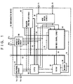
- a semiconductor device 100 comprises a peripheral circuit 10, a CPU 20, a ROM 30, a decoder 40, an EPROM/ICE interface circuit 50, a register 60, a mode switch circuit 70, and a RON read control circuit 80. These circuits are connected by internal buses 12 and signal lines 13 to 16. Signals passing through the signal lines will be hereinafter denoted by the same reference numerals as the corresponding signal lines.
- the peripheral circuit 10 comprises a register, a RAM (not shown), and other circuit. These circuits in the peripheral circuit 10 transmit and receive signals via terminal 11a to 11x.
- the EPROM/ICE interface circuit 50 is an interface circuit for controlling the semiconductor device 100 in an EPROM/ICE mode by an external ICE tool or EPROM (not shown).
- the EPROM/ICE interface circuit 50 has terminals 51a to 51x. In an ICE mode, the ICE tool is connected to the terminals 51a to 51x, so that the operation of the semiconductor device 100 can be controlled by a personal computer or a special device for the semiconductor device 100. In an EPROM mode, the EPROM is connected to the terminals 51a to 51x, so that the semiconductor device 100 operates in accordance with instructions written in the EPROM.
- the register 60 is a register, and determines whether data should be read from the ROM 30 in the EPROM/ICE mode.
- the register 60 receives the data via an internal bus 12. If the register 60 receives a certain data value in the EPROM/ICE mode, the register 60 outputs a high-level signal 15 to the ROM read control circuit 80, so that the data can be read from the ROM 30.
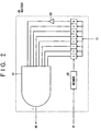
- Fig. 2 illustrates an example of the structure of the register 60.
- the register 60 comprises an AND circuit 61, a decoder 62, and an inverter 63.
- the register 60 When a high-level signal 1 is inputted into each of the input terminals of the AND circuit 61 from an internal bus 12 via the decoder 62, the register 60 outputs a high level signal 15 to the ROM read control circuit 80.
- the mode switch circuit 70 supplies the EPROM/ICE interface circuit 50 and the ROM read control circuit 80 with mode signals based on signals inputted into terminals 71 and 72, thereby determining the operation mode of the semiconductor device 100.
- Fig. 3 illustrates an example of the structure of the mode switch circuit 70.
- the mode switch circuit 70 comprises AND circuits 73 to 75, and inverters 76 and 77.
- the terminals 71 and 72 of the mode switch circuit 70 receive combinations of mode setting signals shown in Fig. 4.
- Fig. 4 shows the relationship between the signals inputted into the mode switch circuit 70 and the signals outputted from the mode switch circuit 70. If low-level signals 0 are inputted into the terminals 71 and 72, for instance, the AND circuits 73 to 75 output low-level signals 0. The output signals are then sent to the CPU 20, the EPROM/ICE interface circuit 50, and the ROM read control circuit 80, thereby making the semiconductor device 100 disabled.
- the AND circuits 73 and 74 output low-level signals, and the AND circuit 75 outputs a high-level signal 1.
- the output signals are then sent to the CPU 20, the EPROM/ICE interface circuit 50, and the ROM read control circuit 80, thereby putting the semiconductor device 100 in a ROM mode in which the semiconductor device 100 operates according to the data contained in the ROM 30 (hereinafter referred to as "In-ROM mode").
- In-ROM mode the data can be read from the ROM 30, regardless of the data value given to the register 60 from the internal bus 12.
- the semiconductor device 100 If a high level signal 1 is inputted into the terminal 71 and a low-level signal 0 is inputted into the terminal 72, the semiconductor device 100 is put in the ICE mode. If high-level signals 1 are inputted into both terminals 71 and 72, the semiconductor device 100 is put in the EPROM mode.
- the ROM read control circuit 80 outputs high-level and low-level signals in accordance with signals sent from the register 60 and the mode switch circuit 70.
- the output signal 14 from the ROM read control circuit 80 is sent to the ROM 30. If the output signal 14 is at high level, data can be read from the ROM 30. If the output signal 14 is at low level, data cannot be read from the ROM 30.
- Fig. 5 illustrates an example of the structure of the ROM read control circuit 80.
- the ROM read control circuit 80 comprises EX(Exclusive)-OR circuits 81 and 82, AND circuits 84 to 86.
- the output signals from the AND circuits 73 to 75 in the mode switch circuits 70 are inputted into the AND circuits 84 to 86 in the ROM read control circuit 80, respectively.
- the AND circuits 84 to 86 also receive a signal 13 from the CPU 20 and a signal 16 from the decoder 40.
- the signal 15 from the register 60 which determines whether the data can be read from the ROM 30 in the EPROM/ICE mode, is inputted into the AND circuit 83 in the ROM read control circuit 80.
- the structures of the register 60, the mode switch circuit 70, and the ROM read control circuit 80 are not limited to those shown in Figs. 2, 3, and 5, but the structures may be modified if necessary.
- Fig. 6 is a timing chart showing the waveforms of signals in the In-ROM mode.
- a low-level signal 0 and a high-level signal 1 are inputted into the terminal 71 and 72, and the mode switch circuit 70 then transmits low level signals 0 to the AND circuits 84 and 85, and a high-level signal 1 to the AND circuit 86 in the ROM read control circuit 80.
- the decoder 40 transmits high-level signals 16 to the AND circuits 84, 85, and 86.
- the EX-OR circuit 81 outputs a low-level signal 14 when the signals 13 transmitted from the CPU 20 to the AND circuits 84 to 86 are at low level, regardless of the level of the signals 15 transmitted from the register 60 to the ROM read control circuit 80.
- the EX-OR circuit 81 outputs a high-level signal 14.
- the ROM 30 receives the high-level signal 14, it becomes possible to read data from the ROM 30.
- Fig. 7 is a timing chart showing the waveforms of signals in the EPROM mode.
- high-level signals 1 are inputted into the terminals 71 and 72, and the mode switch circuit 70 then transmits a high-level signal 1 to the AND circuit 84, and low-level signals 0 to the AND circuits 85 and 86 in the ROM read control circuit 80.
- the decoder 40 transmits high-level signals 16 to the AND circuits 84 to 86. Accordingly, no specific data value is inputted into the register 60 via the internal bus 12.
- the EX-OR circuit 81 When the register 60 transmits a low-level signal 15 to the ROM read control circuit 80, the EX-OR circuit 81 continues to output a low-level signal 14 even if the signal 13 inputted from the CPU20 into the ROM read control circuit 80 changes to a high-level signal. At this point, data cannot be read from the ROM 30.
- the EX-OR circuit 81 when a specific data value is inputted into the register 60 via the internal bus 12 and the register 60 transmits a high-level signal 15 to the ROM read control circuit 80, the EX-OR circuit 81 also transmits a high-level signal 14 if the signal 13 inputted from the CPU 20 to the ROM read control circuit 80 changes to a high-level signal. At this point, it becomes possible to read data from the ROM 30.
- the EX-OR circuit 81 In the ICE mode, as in the EPROM mode, the EX-OR circuit 81 outputs a high-level signal 14 when the signals 13, 15, and 16 are all at high level, thereby enabling data reading from the ROM 30.
- the semiconductor device 100 Since the data cannot be read from the ROM 30 when no specific data value is inputted into the register 60 in the EPROM/ICE mode, it is possible to prevent the ROM data reading against the owner's will.
- the semiconductor device 100 has the In-ROM mode and the EPROM/ICE mode, so that there is no need to develop two semiconductor devices corresponding to both mode. Thus, the semiconductor device 100 can be produced in a shorter period of time, and the production costs of the semiconductor device 100 can also be reduced.
- the data to be inputted into the AND circuit 61 shown in FIG. 2 correspond to the predetermined condition and the data in the claims of the present invention.
- the signals inputted via the terminals 71 and 72 correspond to the mode selecting signals in the claims.
- the signals 14 and 15 correspond to a first signal and a second signal in the claims of the present invention.
Landscapes
- Engineering & Computer Science (AREA)
- General Engineering & Computer Science (AREA)
- Theoretical Computer Science (AREA)
- Computer Hardware Design (AREA)
- Quality & Reliability (AREA)
- Physics & Mathematics (AREA)
- General Physics & Mathematics (AREA)
- Read Only Memory (AREA)
- Semiconductor Integrated Circuits (AREA)
- For Increasing The Reliability Of Semiconductor Memories (AREA)
- Storage Device Security (AREA)
Applications Claiming Priority (2)
| Application Number | Priority Date | Filing Date | Title |
|---|---|---|---|
| JP23901698 | 1998-08-25 | ||
| JP23901698A JP2000068461A (ja) | 1998-08-25 | 1998-08-25 | 半導体装置 |
Publications (2)
| Publication Number | Publication Date |
|---|---|
| EP0989495A1 true EP0989495A1 (de) | 2000-03-29 |
| EP0989495B1 EP0989495B1 (de) | 2003-03-05 |
Family
ID=17038649
Family Applications (1)
| Application Number | Title | Priority Date | Filing Date |
|---|---|---|---|
| EP99116075A Expired - Lifetime EP0989495B1 (de) | 1998-08-25 | 1999-08-17 | Elektronische Schaltung zur Datensicherung in einer Halbleitervorrichtung |
Country Status (5)
| Country | Link |
|---|---|
| US (1) | US6650579B1 (de) |
| EP (1) | EP0989495B1 (de) |
| JP (1) | JP2000068461A (de) |
| KR (1) | KR20000017416A (de) |
| DE (1) | DE69905671T2 (de) |
Families Citing this family (2)
| Publication number | Priority date | Publication date | Assignee | Title |
|---|---|---|---|---|
| KR100442878B1 (ko) * | 2002-07-08 | 2004-08-02 | 삼성전자주식회사 | 온 칩 롬 테스트 장치 및 방법 |
| KR20190029316A (ko) * | 2017-09-12 | 2019-03-20 | 에스케이하이닉스 주식회사 | 마이크로 컨트롤러, 이를 포함하는 메모리 시스템 및 이의 동작방법 |
Citations (2)
| Publication number | Priority date | Publication date | Assignee | Title |
|---|---|---|---|---|
| JPH05265867A (ja) * | 1992-03-23 | 1993-10-15 | Nec Corp | シングルチップマイクロコンピュータ |
| US5526311A (en) * | 1993-12-30 | 1996-06-11 | Intel Corporation | Method and circuitry for enabling and permanently disabling test mode access in a flash memory device |
Family Cites Families (6)
| Publication number | Priority date | Publication date | Assignee | Title |
|---|---|---|---|---|
| JPH0393098A (ja) * | 1989-09-04 | 1991-04-18 | Sharp Corp | 集積回路 |
| US5345413A (en) * | 1993-04-01 | 1994-09-06 | Microchip Technology Incorporated | Default fuse condition for memory device after final test |
| US5386385A (en) * | 1994-01-31 | 1995-01-31 | Texas Instruments Inc. | Method and apparatus for preventing invalid operating modes and an application to synchronous memory devices |
| US6085346A (en) * | 1996-09-03 | 2000-07-04 | Credence Systems Corporation | Method and apparatus for built-in self test of integrated circuits |
| US5959912A (en) * | 1997-04-30 | 1999-09-28 | Texas Instruments Incorporated | ROM embedded mask release number for built-in self-test |
| US6108793A (en) * | 1997-07-18 | 2000-08-22 | Fujitsu Limited | Semiconductor device having timing-stabilization circuit and method of testing such semiconductor device |
-
1998
- 1998-08-25 JP JP23901698A patent/JP2000068461A/ja not_active Withdrawn
-
1999
- 1999-08-17 EP EP99116075A patent/EP0989495B1/de not_active Expired - Lifetime
- 1999-08-17 DE DE69905671T patent/DE69905671T2/de not_active Expired - Fee Related
- 1999-08-20 KR KR1019990034556A patent/KR20000017416A/ko not_active Withdrawn
- 1999-08-23 US US09/377,625 patent/US6650579B1/en not_active Expired - Fee Related
Patent Citations (2)
| Publication number | Priority date | Publication date | Assignee | Title |
|---|---|---|---|---|
| JPH05265867A (ja) * | 1992-03-23 | 1993-10-15 | Nec Corp | シングルチップマイクロコンピュータ |
| US5526311A (en) * | 1993-12-30 | 1996-06-11 | Intel Corporation | Method and circuitry for enabling and permanently disabling test mode access in a flash memory device |
Non-Patent Citations (1)
| Title |
|---|
| PATENT ABSTRACTS OF JAPAN vol. 018, no. 039 (P - 1679) 20 January 1994 (1994-01-20) * |
Also Published As
| Publication number | Publication date |
|---|---|
| JP2000068461A (ja) | 2000-03-03 |
| EP0989495B1 (de) | 2003-03-05 |
| DE69905671D1 (de) | 2003-04-10 |
| KR20000017416A (ko) | 2000-03-25 |
| DE69905671T2 (de) | 2003-10-02 |
| US6650579B1 (en) | 2003-11-18 |
Similar Documents
| Publication | Publication Date | Title |
|---|---|---|
| US6801956B2 (en) | Arrangement with a microprocessor | |
| US6163183A (en) | Multifunction reset for mixed-signal integrated circuits | |
| EP1923788A2 (de) | Mobiles Endgerät mit mehreren CPUs sowie Testsystem und -verfahren für mehrere CPUs | |
| US4989208A (en) | Data processor | |
| US8207761B2 (en) | Semiconductor device and operation mode switch method | |
| WO2004055670A3 (en) | Code download in a system having multiple integrated circuits with jtag capability | |
| US20080010541A1 (en) | Integrated circuit device, debugging tool, debugging system, microcomputer, and electronic instrument | |
| EP0675448A1 (de) | Busschnittstellenschaltung für integrierte Bausteine und Eingang-Ausgangpufferschaltung | |
| EP1233325A2 (de) | Terminalvorrichtung und Verfahren zur Steuerung einer Echtzeituhr | |
| US5767694A (en) | Information processing apparatus with a mode setting circuit | |
| US6650579B1 (en) | Semiconductor device having test and read modes and protection such that ROM data reading is prevented in the test mode | |
| EP0915566A2 (de) | Rücksetzschaltung für Flipflop | |
| US6845496B2 (en) | Semiconductor integrated circuit device using programmable peripheral control | |
| US20060242527A1 (en) | Microprocessor with trace module | |
| US4961191A (en) | Test circuit for logic circuits | |
| JPH0944467A (ja) | マイクロコンピュータ | |
| US20060218445A1 (en) | Semiconductor integrated circuit device, debug system, microcomputer, and electronic apparatus | |
| US20020194510A1 (en) | Apparatus and method for bus power measurement in a digital signal processor | |
| US20040215867A1 (en) | Control chip, circuit and method thereof for inhibiting bus cycle | |
| US5341380A (en) | Large-scale integrated circuit device | |
| US6141717A (en) | Microcomputer having bus isolation means for selectively coupling an external bus to either a memory bus or a peripheral bus for testing of memory and peripheral circuits | |
| KR100253934B1 (ko) | 반도체 집적회로 | |
| CN114759913A (zh) | 接口电路、参数配置的方法、存储介质及电子设备 | |
| JP2002110925A (ja) | システムlsi | |
| JP3071044B2 (ja) | マイクロコンピュータを備える半導体集積回路の試験方法 |
Legal Events
| Date | Code | Title | Description |
|---|---|---|---|
| PUAI | Public reference made under article 153(3) epc to a published international application that has entered the european phase |
Free format text: ORIGINAL CODE: 0009012 |
|
| AK | Designated contracting states |
Kind code of ref document: A1 Designated state(s): DE FR |
|
| AX | Request for extension of the european patent |
Free format text: AL;LT;LV;MK;RO;SI |
|
| AKX | Designation fees paid |
Free format text: DE FR |
|
| 17P | Request for examination filed |
Effective date: 20000927 |
|
| 17Q | First examination report despatched |
Effective date: 20011213 |
|
| GRAH | Despatch of communication of intention to grant a patent |
Free format text: ORIGINAL CODE: EPIDOS IGRA |
|
| GRAH | Despatch of communication of intention to grant a patent |
Free format text: ORIGINAL CODE: EPIDOS IGRA |
|
| GRAA | (expected) grant |
Free format text: ORIGINAL CODE: 0009210 |
|
| AK | Designated contracting states |
Designated state(s): DE FR |
|
| REF | Corresponds to: |
Ref document number: 69905671 Country of ref document: DE Date of ref document: 20030410 Kind code of ref document: P |
|
| PGFP | Annual fee paid to national office [announced via postgrant information from national office to epo] |
Ref country code: FR Payment date: 20030704 Year of fee payment: 5 |
|
| PGFP | Annual fee paid to national office [announced via postgrant information from national office to epo] |
Ref country code: DE Payment date: 20030915 Year of fee payment: 5 |
|
| ET | Fr: translation filed | ||
| PLBE | No opposition filed within time limit |
Free format text: ORIGINAL CODE: 0009261 |
|
| STAA | Information on the status of an ep patent application or granted ep patent |
Free format text: STATUS: NO OPPOSITION FILED WITHIN TIME LIMIT |
|
| 26N | No opposition filed |
Effective date: 20031208 |
|
| PG25 | Lapsed in a contracting state [announced via postgrant information from national office to epo] |
Ref country code: DE Free format text: LAPSE BECAUSE OF NON-PAYMENT OF DUE FEES Effective date: 20050301 |
|
| PG25 | Lapsed in a contracting state [announced via postgrant information from national office to epo] |
Ref country code: FR Free format text: LAPSE BECAUSE OF NON-PAYMENT OF DUE FEES Effective date: 20050429 |
|
| REG | Reference to a national code |
Ref country code: FR Ref legal event code: ST |