EP0983609B1 - Verfahren zur herstellung eines mikrosensors mit mikrogefertigtem silizium - Google Patents
Verfahren zur herstellung eines mikrosensors mit mikrogefertigtem silizium Download PDFInfo
- Publication number
- EP0983609B1 EP0983609B1 EP98925745A EP98925745A EP0983609B1 EP 0983609 B1 EP0983609 B1 EP 0983609B1 EP 98925745 A EP98925745 A EP 98925745A EP 98925745 A EP98925745 A EP 98925745A EP 0983609 B1 EP0983609 B1 EP 0983609B1
- Authority
- EP
- European Patent Office
- Prior art keywords
- silicon
- plate
- width
- thickness
- upper face
- Prior art date
- Legal status (The legal status is an assumption and is not a legal conclusion. Google has not performed a legal analysis and makes no representation as to the accuracy of the status listed.)
- Expired - Lifetime
Links
Images


Classifications
-
- B—PERFORMING OPERATIONS; TRANSPORTING
- B81—MICROSTRUCTURAL TECHNOLOGY
- B81C—PROCESSES OR APPARATUS SPECIALLY ADAPTED FOR THE MANUFACTURE OR TREATMENT OF MICROSTRUCTURAL DEVICES OR SYSTEMS
- B81C1/00—Manufacture or treatment of devices or systems in or on a substrate
- B81C1/00015—Manufacture or treatment of devices or systems in or on a substrate for manufacturing microsystems
- B81C1/00134—Manufacture or treatment of devices or systems in or on a substrate for manufacturing microsystems comprising flexible or deformable structures
- B81C1/0015—Cantilevers
-
- G—PHYSICS
- G01—MEASURING; TESTING
- G01P—MEASURING LINEAR OR ANGULAR SPEED, ACCELERATION, DECELERATION, OR SHOCK; INDICATING PRESENCE, ABSENCE, OR DIRECTION, OF MOVEMENT
- G01P15/00—Measuring acceleration; Measuring deceleration; Measuring shock, i.e. sudden change of acceleration
- G01P15/02—Measuring acceleration; Measuring deceleration; Measuring shock, i.e. sudden change of acceleration by making use of inertia forces using solid seismic masses
- G01P15/08—Measuring acceleration; Measuring deceleration; Measuring shock, i.e. sudden change of acceleration by making use of inertia forces using solid seismic masses with conversion into electric or magnetic values
- G01P15/0802—Details
-
- G—PHYSICS
- G01—MEASURING; TESTING
- G01P—MEASURING LINEAR OR ANGULAR SPEED, ACCELERATION, DECELERATION, OR SHOCK; INDICATING PRESENCE, ABSENCE, OR DIRECTION, OF MOVEMENT
- G01P15/00—Measuring acceleration; Measuring deceleration; Measuring shock, i.e. sudden change of acceleration
- G01P15/02—Measuring acceleration; Measuring deceleration; Measuring shock, i.e. sudden change of acceleration by making use of inertia forces using solid seismic masses
- G01P15/08—Measuring acceleration; Measuring deceleration; Measuring shock, i.e. sudden change of acceleration by making use of inertia forces using solid seismic masses with conversion into electric or magnetic values
- G01P15/125—Measuring acceleration; Measuring deceleration; Measuring shock, i.e. sudden change of acceleration by making use of inertia forces using solid seismic masses with conversion into electric or magnetic values by capacitive pick-up
-
- B—PERFORMING OPERATIONS; TRANSPORTING
- B81—MICROSTRUCTURAL TECHNOLOGY
- B81B—MICROSTRUCTURAL DEVICES OR SYSTEMS, e.g. MICROMECHANICAL DEVICES
- B81B2201/00—Specific applications of microelectromechanical systems
- B81B2201/02—Sensors
- B81B2201/0228—Inertial sensors
- B81B2201/0235—Accelerometers
-
- B—PERFORMING OPERATIONS; TRANSPORTING
- B81—MICROSTRUCTURAL TECHNOLOGY
- B81C—PROCESSES OR APPARATUS SPECIALLY ADAPTED FOR THE MANUFACTURE OR TREATMENT OF MICROSTRUCTURAL DEVICES OR SYSTEMS
- B81C2201/00—Manufacture or treatment of microstructural devices or systems
- B81C2201/05—Temporary protection of devices or parts of the devices during manufacturing
- B81C2201/053—Depositing a protective layers
Definitions
- the invention relates to the production of microsensors machined from silicon, in particular accelerometers for assistance applications aircraft navigation, and pressure sensors.
- sensors and in particular sensors made by superimposing three silicon plates assembled by bonding or welding, the plates being partly machined before assembly and partly after assembly.
- the central plate includes directly active mechanical elements, that is to say on which the acceleration is exerted in the case of a accelerometer, pressure in the case of a pressure sensor; she also includes electrical components necessary for operation.
- the upper and lower plates frame the central plate and carry possibly electrical elements necessary for operation, in complement of the electrical elements of the central plate (in particular electrical connections).
- One of the main problems in the manufacture of these sensors is the etching of certain elements of the central plate, and especially elements that require high precision of micro-machining due to their role in the sensor.
- suspension elements of the micro-sensor i.e. the mechanical elements which undergo movements or constraints depending on the parameters we are trying to measure (accelerations, pressure, etc.).
- the problem lies in the etching of the elements of suspension and resonant beam.
- a pressure comprising a thin plate under pressure and transmitting its deformations to the ends of a resonant beam
- the problem mainly lies in the etching of the resonant beam and elements by which it is connected to the thin plate.
- the machining of the elements of the central plate is made particularly difficult because it must be planned, in addition to the engraving of the active elements, other engravings, including very deep engravings up to a complete separation between an active central area and a peripheral frame, these deep engravings to be executed without damaging the partial engravings of the elements assets.
- the manufacturing process must take into account numerous constraints and the object of the present invention is to propose perform certain manufacturing steps in an advantageous manner while being consistent with the many other steps that must be executed to arrive at an operational sensor.
- US-A-5,415,726 describes the manufacture of an accelerometer in which a seismic mass is cut in a first substrate, the seismic mass being connected to a frame by a continuous membrane having the final thickness of the beam. After soldering of this first substrate to a second, the membrane is selectively etched to form one (or more) beams.
- fasteners temporary are kept between the frame and the active elements, until the assembly of the two plates, and these temporary fasteners are not eliminated only after assembly, during the directive attack operation of the silicon.
- an accelerometer comprising a seismic mass connected to a foot not only by the beam but also by arms of suspension located in the median plane of the thickness of the first plate
- the manufacturing process according to the invention is applicable to various micro-machined silicon sensors and will be described about an accelerometer whose general structure is shown in Figures 1 and 2.
- the accelerometer consists of the superposition of three machined conductive silicon plates, 10, 20, 30, welded together remaining separated from each other by layers of silicon oxide 15 and 25.
- Figure 2 shows a top view of the central plate 30, in which a seismic mass 31 has been machined in particular, a resonant beam 32 connected to the seismic mass, and suspension arms side 33 and 34.
- the central plate has a structure overall symmetrical about a vertical median plane passing through the middle of the resonant beam along it.
- the lateral suspension arms 33 and 34 are arranged symmetrically on either side of this plane of symmetry.
- the central plate 30 is actually made up of two parts very distinct which are electrically isolated from each other and which for this reason were completely physically separated from each other by etching during the manufacture of the accelerometer.
- the first part 35 is a continuous peripheral frame surrounding the entire second part which is the active part 36 of the accelerometer.
- the peripheral frame 35 serves essentially connecting spacer between the bottom plate 10 and the upper plate 20 to keep these two plates apart one of the other. But it also serves as electrical shielding between the plates 10 and 20.
- the active part 36 of the central plate is entirely located between the lower and upper plates, and inside the peripheral frame 35.
- the three silicon plates are electrically conductive, because they directly participate in the electrical functioning of the micro-accelerometer; they are preferably made of highly doped P-type silicon (boron doping).
- Metal contacts are formed by deposition and engraving (aluminum for example) on the bottom plate (contact 13 on the edge of the plate), on the peripheral frame 35 of the central plate (contact 38 on the outer edge of the frame), and on the upper plate (contact 22 on the edge of the plate), to connect each of these plates to a resonant electrical circuit to which the structure described is connected.
- the accelerations undergone by the seismic mass are translated by a greater or lesser tension of the resonant beam.
- the capacitor formed by this beam and the upper silicon plate is placed in a resonant circuit whose resonant frequency depends on the voltage therefore exerted acceleration.
- a compensation diode temperature variations are expected in the resonant circuit in which acts the capacitor.
- An easy solution is to provide a type of diffusion N, forming a diffused region 26, in the upper part of the plate upper 20, with a contact electrode 27 deposited on this region diffused 26.
- This contact electrode is produced by metallization (aluminum for example) which joins (in a way not visible on the figures) an edge of the top plate to allow connection with outside the structure.
- the metallization is deposited above a insulating layer 28 (silicon oxide for example) which covers the assembly of the upper plate with the exception of the contacting areas with the plate and with the diffused region 26.
- FIG. 3 shows a general flowchart of the different manufacturing steps. Some steps are performed separately on the lower plate, the upper plate or the central plate, before the assembly of these plates with the others. Then steps are carried out after assembly of the bottom plate and the central plate. Finally steps are carried out after assembly of the three plates.
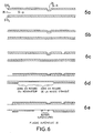
- the lower plate 10 undergoes steps oxidation, deposition of silicon nitride, photogravure of oxide silicon and silicon nitride, silicon nitride being used as oxide etching mask, then silicon etching on the face upper for the definition of the stops 11, 12 and on the lower face for the definition of openings 14 and 17.
- the upper plate 20 undergoes meanwhile operations oxidation, etching of silicon oxide, doping for the manufacture of the diode (region 26); then silicon nitride deposition operations, photogravure of silicon oxide and nitride, and successive engravings silicon on the underside to define the stops 23, 24, and the surface of region 21 forming a capacitor electrode.
- the central plate undergoes during this time the operations following: oxidation, deposition of silicon nitride, oxide etching, etchings successive silicon chemicals with successive masks, to define successively the configuration of the foot 37, of the seismic mass 31, of the suspension arms 33, 34, and the thickness of the beam 32 (but not its final width).
- the bottom plate and the central plate are then welded together.
- a final etching operation of the resonant beam and complete separation of the spacer frame 35 is then carried out.
- the upper plate is welded to the plate central, the metallizations are deposited on the outer faces of all, no metallization being necessary in the enclosed space by the upper and lower plates inside the spacer frame 35.
- the cavity formed in this space is hermetically closed by a sealing in indium or indium-based alloy.
- the nitride layer of the upper face is etched according to a pattern defining the area opposite the seismic mass, reserving the nitride at the location of the lower stops 11, 12 of Figure 1; and we attack the oxide over part of its depth where the nitride was removed (figure 4b).
- the nitride layer of the underside is etched in a pattern defining the opening 17 and attacking the oxide on part of its depth in this pattern ( Figure 4c).
- the nitride is etched again on the underside in a pattern defining the contact opening 14, and the oxide is completely removed in this region, having previously masked the opening 17 and the face upper plate to store the oxide ( Figure 4d).
- Top plate 20
- the upper plate 20 is oxidized on its two faces, a opening is formed in the oxide of the upper face to define the diode temperature compensation, and the silicon area 26 thus discovered is doped, for example with phosphorus ( Figure 6a).
- Zone 26 is oxidized during or after the doping operation ( Figure 6b).
- Two openings are photo-etched in the oxide layer of the upper face, respectively a diode access opening and a opening for the metallization 22 of access to the plate (FIG. 6c).
- Both sides of the plate are covered with nitride of silicon and nitride on the underside is photo-etched to define the areas of silicon that must be dug to move them away from the central plate in order to reduce the parasitic capacities between central plate and plate higher; in these zones, as well as in zone 21 which will be next to the resonant beam, the silicon oxide is removed on part of its thickness only ( Figure 6d). On the upper side, the oxide is removed over its entire thickness on one edge of the plate only.
- the oxide undergoes an operation photogravure and is removed on the one hand opposite the seismic mass, except where it is necessary to define upper stops 23, 24, and on the other hand on the edge of the plate; it is not removed in the area which will be opposite the resonant beam (figure 6e).
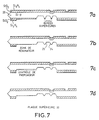
- the silicon is attacked chemically where it is stripped, namely on the edge of the plate (on both sides) and, on the underside, in the zone located opposite the seismic mass with the exception of the stops 23, 24 which are thus produced (FIG. 7a).
- the exposed silicon oxide is photo-etched (resin mask) on the upper side to reduce its thickness approximately everywhere except on the lateral edges of the resonant beam, on the foot 37, and on the spacer frame 35 ( Figure 8b).
- the silicon oxide is photo-etched to reduce its thickness everywhere except at the point of mass seismic, the foot 37 and the spacer frame 35 (Figure 8c).
- a silicon oxide photogravure mask is put on place on the upper side to define a silicon protection pattern above the suspension arms 33, 34 and temporary fasteners between frame 35 and rest of the central plate, attachments which will be removed after assembly of the central plate on the lower plate.
- Oxide silicon is removed to a thickness of a few tenths of a micrometer to strip the silicon on the upper face of the central plate, with the exception of the following areas where it remains protected by oxide: frame spacer 35, resonant beam 32 and lateral edges on either side of the beam, seismic mass, suspension arm 33, temporary fasteners 35 '. ( Figure 8d).
- a silicon oxide photogravure mask is set up on the underside, identical to that of the upper side at except that silicon should not be protected below the resonant beam 32 nor on its edges.
- the silicon oxide is removed to strip the silicon except at the place of the frame 35, of its temporary fasteners, of the seismic mass, and of the suspension arms 33 (FIG. 9a).
- the silicon is etched by chemical attack on both sides at the times, to start the engraving where it is stripped (figure 9b).
- the silicon can then be attacked again to give the resonant beam the desired final thickness (figure 10c).
- the next step is to remove part of the thickness of the oxide present on the underside, by vertical directive etching towards the high, which removes the oxide under the suspension arms and under the fasteners provisional 35 ', without continuing to engrave enough to remove the oxide below the spacer frame 35 and the seismic mass 31 ( Figure 10d).
- the central plate 30 is placed in contact by its underside with the upper face of the lower plate 10 and the assembly is subjected to oxidizing annealing followed by annealing in a neutral atmosphere.
- the plates are solder and the bare silicon parts are covered with a thin layer silicon oxide ( Figure 11a).
- the engraving is preferably a vertical directive engraving (by plasma) but it can also be a non-directive chemical etching; in in the latter case, the width of the arm defining the beam 32 must take account of the slight under-etching resulting from the chemical attack.
- the assembly of the two plates is subjected to an operation of partial deoxidation which eliminates the oxide everywhere (without eliminating the oxide present under the spacer frame 35 and under the foot 37 at the junction of the welded plates).
- partial deoxidation which eliminates the oxide everywhere (without eliminating the oxide present under the spacer frame 35 and under the foot 37 at the junction of the welded plates).
- the oxide present between the stops 11,12 and the seismic mass is eliminated due to the narrowness of the stops.
- the oxide present at the bottom of the openings 14 and 17 is also removed, and the oxide etching is continued until the silicon is stripped from the plate central in the bottom of the opening 14.
- there is more oxide on the active parts of the central plate i.e. on the seismic mass, beam, and suspension arms ( Figure 11d).
- the resonant beam 32 has its final dimensions both in width and in thickness. The same is true of the arms of suspension 33, and of the seismic mass 31.
- the upper plate is then attached to the central plate by vacuum welding at around 1000 ° C. Vacuum welding allows immediately empty the closed cavity containing the mass seismic and the resonant beam.
- the opening 17 is always closed at this stage by a certain residual thickness of silicon ( Figure 12a).
- Figure 12 shows the actual configuration of the sensor, i.e. the different parts are placed one by one compared to others at their actual functional location, unlike what which was done to describe the previous operations.
- a metallic deposition is carried out by evaporation, on the faces external of the sensor, then an engraving to delimit the contacts and deposits metal to be left on each plate: contacts 22 and 27 on the plate upper, possible connection to bring contact 27 back to the edge of the plaque; contact 38 on the central plate; contact 13 on the plate lower; contact 16 on the central plate through the opening 14 of the bottom plate. All these contacts can be in evaporated aluminum under vacuum.
- a separate deposit of chromium-gold alloy 19 can be made in opening 17, in anticipation of a subsequent indium weld ( Figure 12b).
- the senor can be tested by test under spikes, all having its cavity closed and vacuum, which is very important.
- the next operation is a drilling of the silicon membrane closing the opening 17.
- the drilling is done by laser (figure 12c).
- the cavity is then closed by an indium ball, under vacuum, to arrive at the structure represented in figure 1.
- a test under points can still be done at this point.
- the manufacturing operations have been described in connection with a accelerometer, but transposition to other types of sensors is easy. The differences would typically be as follows for a pressure: there is no suspended seismic mass and the resonant beam is attached between two fixed feet such as foot 37. The bottom plate is very thinned in the region separating these two feet, and the deformations of the plate due to external pressure result in a stress of traction on the resonant beam.
- the manufacturing operations would broadly the same, particularly those relating to machining in thickness and width of the resonant beam.
Claims (5)
- Verfahren zur Mikrobearbeitung eines Trägers (32) eines Mikrosensors, der wenigstens zwei Platten (10, 30) umfaßt, wovon wenigstens die erste (30) aus mikrobearbeitetem Silicium besteht, wobei dieses Verfahren dadurch gekennzeichnet ist, daß:durch Mikrobearbeitung von Silicium auf der ersten Platte (30) ein Träger mit einer Dicke, die gleich der gewünschten Enddicke ist, und mit einer Breite, die größer als die gewünschte Endbreite ist, hergestellt wird, wobei der Träger auf seiner oberen Fläche mit einer Maske beschichtet wird, die die gewünschte Endbreite definiert;die beiden Platten zusammengefügt werden;die untere Fläche und diejenigen Teile der oberen Fläche des Trägers, die nicht mit der Maske beschichtet sind, oxidiert werden, um sie mit einer dünnen Schutzschicht zu überziehen;diese dünne Schutzschicht auf der oberen Fläche durch vertikale direkte Ätzung abgehoben wird, ohne daß die bereits vorhandene Maske abgehoben wird;das Silicium in der durch den vorhergehenden Vorgang freigelegten Zone mittels einer Ätzung durch die obere Fläche angegriffen wird, bis der gesamte durch die Maske nicht geschützte Teil des Trägers entfernt ist und somit der Träger mit der gewünschten Breite gebildet ist.
- Verfahren nach Anspruch 1, dadurch gekennzeichnet, daß der Vorgang des Ätzens des Siliciums in der freigelegten Zone eine vertikale direkte Ätzung ist.
- Verfahren nach einem der Ansprüche 1 und 2, dadurch gekennzeichnet, daß die Bearbeitung des Trägers vor dem Zusammenfügen der Platten die folgenden Vorgänge umfaßt:Ablagern einer Schicht zum Schutz vor der Ätzung von Silicium auf einer Breite, die größer als die gewünschte Breite des Trägers ist, wobei diese Schicht auf einer Breite, die der gewünschten Endbreite für den Träger entspricht, dicker ist;Angreifen des Siliciums zugleich durch die obere Fläche und die untere Fläche in einem oder in mehreren Schritten, bis dem Träger die gewünschte Enddicke verliehen ist;Abheben der Schutzschicht an den Rändern des Trägers beiderseits der gewünschten Endbreite, wobei derjenige Teil der Schutzschicht beibehalten wird, der die gewünschte Endbreite besitzt.
- Verfahren nach Anspruch 3, das auf die Herstellung eines Beschleunigungsmessers angewendet wird, der eine seismische Masse (31) umfaßt, die durch den Träger und durch Aufhängungsarme (32, 34), die sich in der Mittelebene der Dicke der ersten Platte (30) befinden, mit einem Fuß verbunden ist, dadurch gekennzeichnet, daß der Angriff des Siliciums zugleich durch die obere Fläche und durch die untere Fläche in der folgenden Weise erfolgt: Ausführen eines Angriffs in einem ersten Schritt, bis die Aufhängungsarme eine gewünschte Dicke erreicht haben, Oxidieren dieser Arme, um sie zu schützen, und Fortsetzen des Angriffs des Siliciums in einem zweiten Schritt, ohne die somit geschützten Aufhängungsarme anzugreifen.
- Verfahren nach einem der Ansprüche 1 bis 4, dadurch gekennzeichnet, daß die Silicium-Platte mikrobearbeitet wird, um einen Umfangsdistanzrahmen (35) zu definieren, der von einem aktiven Teil innerhalb dieses Rahmens vollständig getrennt ist, wobei der Träger einen Teil des aktiven Teils bildet, dadurch gekennzeichnet, daß ein abschließender Trennvorgang zwischen dem Rahmen und dem aktiven Teil durch Abheben von Silicium während des Schrittes des Ätzens von Silicium, der dem Träger seine gewünschte Endbreite verleiht, erfolgt.
Applications Claiming Priority (3)
| Application Number | Priority Date | Filing Date | Title |
|---|---|---|---|
| FR9706333 | 1997-05-23 | ||
| FR9706333A FR2763745B1 (fr) | 1997-05-23 | 1997-05-23 | Procede de fabrication d'un micro-capteur en silicium usine |
| PCT/FR1998/000998 WO1998053483A1 (fr) | 1997-05-23 | 1998-05-19 | Procede de fabrication d'un micro-capteur en silicium usine |
Publications (2)
| Publication Number | Publication Date |
|---|---|
| EP0983609A1 EP0983609A1 (de) | 2000-03-08 |
| EP0983609B1 true EP0983609B1 (de) | 2002-01-02 |
Family
ID=9507181
Family Applications (1)
| Application Number | Title | Priority Date | Filing Date |
|---|---|---|---|
| EP98925745A Expired - Lifetime EP0983609B1 (de) | 1997-05-23 | 1998-05-19 | Verfahren zur herstellung eines mikrosensors mit mikrogefertigtem silizium |
Country Status (6)
| Country | Link |
|---|---|
| US (1) | US6251698B1 (de) |
| EP (1) | EP0983609B1 (de) |
| DE (1) | DE69803377T2 (de) |
| FR (1) | FR2763745B1 (de) |
| NO (1) | NO995731L (de) |
| WO (1) | WO1998053483A1 (de) |
Families Citing this family (17)
| Publication number | Priority date | Publication date | Assignee | Title |
|---|---|---|---|---|
| DE10104868A1 (de) | 2001-02-03 | 2002-08-22 | Bosch Gmbh Robert | Mikromechanisches Bauelement sowie ein Verfahren zur Herstellung eines mikromechanischen Bauelements |
| JP4890689B2 (ja) * | 2001-07-24 | 2012-03-07 | オリンパス株式会社 | 三次元構造体の製造方法及び揺動体の製造方法 |
| FR2834055B1 (fr) * | 2001-12-20 | 2004-02-13 | Thales Sa | Capteur inertiel micro-usine pour la mesure de mouvements de rotation |
| FR2838423B1 (fr) * | 2002-04-12 | 2005-06-24 | Thales Sa | Procede de fabrication d'une microstructure comportant une cavite sous vide et microstructure correspondante |
| US6959583B2 (en) * | 2002-04-30 | 2005-11-01 | Honeywell International Inc. | Passive temperature compensation technique for MEMS devices |
| US8039443B2 (en) * | 2002-11-21 | 2011-10-18 | Archemix Corporation | Stabilized aptamers to platelet derived growth factor and their use as oncology therapeutics |
| FR2856789B1 (fr) * | 2003-06-27 | 2005-08-26 | Thales Sa | Gyrometre a masse vibrante |
| FR2880731B1 (fr) * | 2005-01-11 | 2007-04-27 | Commissariat Energie Atomique | Composant, notamment avec des elements actifs, et procede de realisation d'un tel composant |
| DE102005015584B4 (de) * | 2005-04-05 | 2010-09-02 | Litef Gmbh | Verfahren zur Herstellung eines mikromechanischen Bauteils |
| US8217473B2 (en) | 2005-07-29 | 2012-07-10 | Hewlett-Packard Development Company, L.P. | Micro electro-mechanical system packaging and interconnect |
| FR2941533B1 (fr) | 2009-01-23 | 2011-03-11 | Commissariat Energie Atomique | Capteur inertiel ou resonnant en technologie de surface, a detection hors plan par jauge de contrainte. |
| FR2941525B1 (fr) * | 2009-01-23 | 2011-03-25 | Commissariat Energie Atomique | Gyrometre en technologie de surface, a detection hors plan par jauge de contrainte. |
| CN102602879B (zh) * | 2011-11-23 | 2016-01-06 | 中国计量学院 | 谐振式加速度计谐振梁和支撑梁的二步腐蚀制造方法 |
| JPWO2013089079A1 (ja) * | 2011-12-12 | 2015-04-27 | 株式会社村田製作所 | 加速度センサ |
| KR101540154B1 (ko) * | 2013-10-04 | 2015-07-28 | 삼성전기주식회사 | 각속도 센서 및 그의 제조방법 |
| JP6575212B2 (ja) * | 2015-08-07 | 2019-09-18 | セイコーエプソン株式会社 | 電子デバイス、電子デバイスの製造方法、電子機器、および移動体 |
| JP7146499B2 (ja) * | 2018-07-17 | 2022-10-04 | 東京計器株式会社 | 3次元構造部材の製造方法、加速度ピックアップ部材の製造方法、加速度ピックアップ部材、及び加速度センサ |
Family Cites Families (6)
| Publication number | Priority date | Publication date | Assignee | Title |
|---|---|---|---|---|
| US5006202A (en) * | 1990-06-04 | 1991-04-09 | Xerox Corporation | Fabricating method for silicon devices using a two step silicon etching process |
| EP0468071B1 (de) * | 1990-07-25 | 1994-09-14 | International Business Machines Corporation | Methode zur Herstellung von mikromechanischen Sensoren für AFM/STM/MFM-Profilometrie und mikromechanischer AFM/STM/MFM-Sensorkopf |
| FR2687783B1 (fr) * | 1992-02-20 | 1994-05-20 | Sextant Avionique | Micro-capteur de pression. |
| FR2700003B1 (fr) * | 1992-12-28 | 1995-02-10 | Commissariat Energie Atomique | Procédé de fabrication d'un capteur de pression utilisant la technologie silicium sur isolant et capteur obtenu. |
| US5415726A (en) * | 1993-12-21 | 1995-05-16 | Delco Electronics Corporation | Method of making a bridge-supported accelerometer structure |
| US5484073A (en) * | 1994-03-28 | 1996-01-16 | I/O Sensors, Inc. | Method for fabricating suspension members for micromachined sensors |
-
1997
- 1997-05-23 FR FR9706333A patent/FR2763745B1/fr not_active Expired - Fee Related
-
1998
- 1998-05-19 WO PCT/FR1998/000998 patent/WO1998053483A1/fr active IP Right Grant
- 1998-05-19 DE DE69803377T patent/DE69803377T2/de not_active Expired - Fee Related
- 1998-05-19 US US09/424,223 patent/US6251698B1/en not_active Expired - Lifetime
- 1998-05-19 EP EP98925745A patent/EP0983609B1/de not_active Expired - Lifetime
-
1999
- 1999-11-22 NO NO995731A patent/NO995731L/no not_active Application Discontinuation
Also Published As
| Publication number | Publication date |
|---|---|
| WO1998053483A1 (fr) | 1998-11-26 |
| US6251698B1 (en) | 2001-06-26 |
| NO995731L (no) | 2000-01-21 |
| DE69803377D1 (de) | 2002-02-28 |
| EP0983609A1 (de) | 2000-03-08 |
| FR2763745B1 (fr) | 1999-08-27 |
| FR2763745A1 (fr) | 1998-11-27 |
| NO995731D0 (no) | 1999-11-22 |
| DE69803377T2 (de) | 2002-09-26 |
Similar Documents
| Publication | Publication Date | Title |
|---|---|---|
| EP0983609B1 (de) | Verfahren zur herstellung eines mikrosensors mit mikrogefertigtem silizium | |
| EP0605300B1 (de) | Verfahren zur Herstellung von Beschleunigungsmessern mittels der "Silizium auf Isolator"-Technologie | |
| EP0754953B1 (de) | Verfahren zur Herstellung einer Struktur mit einer mittels Anschlägen auf Abstand von einem Substrat gehaltenen Nutzschicht, sowie Verfahren zur Loslösung einer solchen Schicht | |
| EP1834924B1 (de) | Einkapselung in einem hermetisch abgeschlossenen Hohlraum eines mikroelektronischen Bauteiles, insbesondere eines MEMS | |
| EP0605302B1 (de) | Herstellungsverfahren für Druckwandler mittels der Silicium auf Isolation Technologie sowie derart hergestellte Wandler | |
| EP0983517B1 (de) | Mikromechanischer beschleunigungsmesser mit kapazitivem resonator | |
| EP2599746B1 (de) | Verfahren zur Herstellung einer Struktur mit mindestens einem aus mehreren Dicken bestehenden aktiven Teil | |
| EP1108677A1 (de) | Hermetische In-Situ-Gehäusungsmethode von Mikrosystemen | |
| EP2599745B1 (de) | Verfahren zum Herstellen eines MEMS Bauteil mit bewegliche Teile unterschiedlicher Dicke | |
| EP3476284B1 (de) | Biokompatibler integrierter monolithischer sensor, insbesondere für eine aktive implantierbare medizinische vorrichtung | |
| FR2992467A1 (fr) | Procede de realisation d'un composant a contact electrique traversant et composant obtenu | |
| EP0866972B1 (de) | Beschleunigungssensor und verfahren zu seiner herstellung | |
| EP3975584A1 (de) | Verfahren zur herstellung eines elektroakustischen transducers | |
| EP3728108B1 (de) | Verwendung einer entkopplungsstruktur zur montage eines bauteils mit einem gehäuse | |
| EP0950172A1 (de) | Verfahren zur herstellung eines aufgehängten elementes in einer mikromechanischen struktur | |
| EP3218302A1 (de) | Verfahren zur herstellung einer elektromechanischen vorrichtung sowie entsprechende vorrichtung | |
| EP1325886B1 (de) | Verfahren zum Verstärken einer mechanischen Mikrostruktur | |
| EP0611221B1 (de) | Kapazitiver Microsensor mit geringer Fremdkapazität und Herstellungsverfahren | |
| EP3633336B1 (de) | Pyroelektrische detektionsvorrichtung mit starrer membran | |
| EP0467810B1 (de) | Struktur und Verfahren zur Versiegelung eines Glas/Siliziumgefässes | |
| WO2002076881A1 (fr) | Procede de fabrication d'une structure a membrane micro-usinee | |
| WO2002091556A1 (fr) | Actionneur electrostatique |
Legal Events
| Date | Code | Title | Description |
|---|---|---|---|
| PUAI | Public reference made under article 153(3) epc to a published international application that has entered the european phase |
Free format text: ORIGINAL CODE: 0009012 |
|
| 17P | Request for examination filed |
Effective date: 19991118 |
|
| AK | Designated contracting states |
Kind code of ref document: A1 Designated state(s): CH DE FR GB LI |
|
| GRAG | Despatch of communication of intention to grant |
Free format text: ORIGINAL CODE: EPIDOS AGRA |
|
| RAP1 | Party data changed (applicant data changed or rights of an application transferred) |
Owner name: THALES AVIONICS S.A. |
|
| 17Q | First examination report despatched |
Effective date: 20010329 |
|
| GRAG | Despatch of communication of intention to grant |
Free format text: ORIGINAL CODE: EPIDOS AGRA |
|
| GRAH | Despatch of communication of intention to grant a patent |
Free format text: ORIGINAL CODE: EPIDOS IGRA |
|
| GRAH | Despatch of communication of intention to grant a patent |
Free format text: ORIGINAL CODE: EPIDOS IGRA |
|
| GRAA | (expected) grant |
Free format text: ORIGINAL CODE: 0009210 |
|
| REG | Reference to a national code |
Ref country code: GB Ref legal event code: IF02 |
|
| AK | Designated contracting states |
Kind code of ref document: B1 Designated state(s): CH DE FR GB LI |
|
| REG | Reference to a national code |
Ref country code: CH Ref legal event code: EP |
|
| REF | Corresponds to: |
Ref document number: 69803377 Country of ref document: DE Date of ref document: 20020228 |
|
| GBT | Gb: translation of ep patent filed (gb section 77(6)(a)/1977) |
Effective date: 20020328 |
|
| PLBE | No opposition filed within time limit |
Free format text: ORIGINAL CODE: 0009261 |
|
| STAA | Information on the status of an ep patent application or granted ep patent |
Free format text: STATUS: NO OPPOSITION FILED WITHIN TIME LIMIT |
|
| 26N | No opposition filed | ||
| PGFP | Annual fee paid to national office [announced via postgrant information from national office to epo] |
Ref country code: DE Payment date: 20050512 Year of fee payment: 8 |
|
| PGFP | Annual fee paid to national office [announced via postgrant information from national office to epo] |
Ref country code: CH Payment date: 20050517 Year of fee payment: 8 |
|
| PG25 | Lapsed in a contracting state [announced via postgrant information from national office to epo] |
Ref country code: LI Free format text: LAPSE BECAUSE OF NON-PAYMENT OF DUE FEES Effective date: 20060531 Ref country code: CH Free format text: LAPSE BECAUSE OF NON-PAYMENT OF DUE FEES Effective date: 20060531 |
|
| PG25 | Lapsed in a contracting state [announced via postgrant information from national office to epo] |
Ref country code: DE Free format text: LAPSE BECAUSE OF NON-PAYMENT OF DUE FEES Effective date: 20061201 |
|
| REG | Reference to a national code |
Ref country code: CH Ref legal event code: PL |
|
| PGFP | Annual fee paid to national office [announced via postgrant information from national office to epo] |
Ref country code: GB Payment date: 20080521 Year of fee payment: 11 |
|
| GBPC | Gb: european patent ceased through non-payment of renewal fee |
Effective date: 20090519 |
|
| PG25 | Lapsed in a contracting state [announced via postgrant information from national office to epo] |
Ref country code: GB Free format text: LAPSE BECAUSE OF NON-PAYMENT OF DUE FEES Effective date: 20090519 |
|
| REG | Reference to a national code |
Ref country code: FR Ref legal event code: PLFP Year of fee payment: 19 |
|
| REG | Reference to a national code |
Ref country code: FR Ref legal event code: PLFP Year of fee payment: 20 |
|
| PGFP | Annual fee paid to national office [announced via postgrant information from national office to epo] |
Ref country code: FR Payment date: 20170427 Year of fee payment: 20 |