EP0977355B1 - Dispositif et méthode pour limiter les crêtes d'un signal - Google Patents
Dispositif et méthode pour limiter les crêtes d'un signal Download PDFInfo
- Publication number
- EP0977355B1 EP0977355B1 EP99305709A EP99305709A EP0977355B1 EP 0977355 B1 EP0977355 B1 EP 0977355B1 EP 99305709 A EP99305709 A EP 99305709A EP 99305709 A EP99305709 A EP 99305709A EP 0977355 B1 EP0977355 B1 EP 0977355B1
- Authority
- EP
- European Patent Office
- Prior art keywords
- signal
- peak
- extrema
- delayed
- input
- Prior art date
- Legal status (The legal status is an assumption and is not a legal conclusion. Google has not performed a legal analysis and makes no representation as to the accuracy of the status listed.)
- Expired - Lifetime
Links
Images


Classifications
-
- H—ELECTRICITY
- H03—ELECTRONIC CIRCUITRY
- H03K—PULSE TECHNIQUE
- H03K5/00—Manipulating of pulses not covered by one of the other main groups of this subclass
- H03K5/01—Shaping pulses
- H03K5/08—Shaping pulses by limiting; by thresholding; by slicing, i.e. combined limiting and thresholding
-
- H—ELECTRICITY
- H03—ELECTRONIC CIRCUITRY
- H03G—CONTROL OF AMPLIFICATION
- H03G11/00—Limiting amplitude; Limiting rate of change of amplitude ; Clipping in general
Definitions
- the present invention relates to a device and method for limiting peaks of a signal and, more particularly, to a device and method for reducing the peak-to-average (P/A) ratio of an input signal without generating significant out-of-band emissions.
- P/A peak-to-average
- Power amplifiers have non-linear characteristics.
- the cost of power amplifiers is determined by the size of their linear range.
- the non-linear characteristic of conventional power amplifiers causes out-of-band spectral artifacts, e.g., spectrum distortions, splatters, spectrum spreading, etc.
- the P/A ratio of the input signal is reduced, allowing the amplifier to output a large average power.
- a hard clipping process is one of the conventional ways to reduce the P/A ratio of an input signal.
- the effect of the hard clipping process is that a noise-like signal is added to the input signal to generate a hard clipped signal.
- the algorithm of the hard clipped signal is as follows, wherein V in represents the input signal, V clip represents the clipping threshold signal, and V out represents the hard clipped signal.
- a hard clipped signal has abrupt edges and sharp peaks.
- the abrupt nature of the hard clipping process and the short time duration of clipped edges generate significant out-of-band spectral artifacts, such as spectrum distortions, splatter, and spectrum spreading.
- an input signal whose spectrum is illustrated in Fig. 1
- the effect in the frequency domain is to add the spectrum of a noise-like signal, shown in Fig. 2A, to the input signal spectrum of Fig. 1.
- the spectrum of the final result of the hard clipping process is then as shown in Fig. 2B.
- the spectrum response of the input signal outside of about 0.3 frequency units is low, the spectrum of the hard clipped signal outside of about 0.3 frequency units is much higher than that of the input signal. Therefore, the hard clipping process is generally undesirable in reducing the P/A ratio of an input signal.
- a window clipping process discussed in U.S. Patent No. 5,287,387 is another conventional method of reducing the P/A ratio of a signal.
- an attenuating window signal is multiplied with the input signal to generate an attenuated signal.
- Portions of the attenuating window signal corresponding to the peak areas of the input signal have a value of less than one, and all other portions have a value of one. Therefore, when the attenuating window signal is multiplied with the input signal, the peak areas of the input signal is reduced, and all other areas remain the same.
- multiplying the signal in the time domain is equivalent to convolving the spectrum of the input signal with the window spectrum in the frequency domain.
- the window clipping process introduces undesirable spectrum spreading while attempting to reduce the splatter and the P/A ratio of the input signal, and thus, fails to adequately address the problems of the conventional clipping processes.
- the present invention is directed to an improved method and device for limiting peaks of an input signal.
- the method and device isolate peaks of an input signal based on a clipping threshold voltage, generate an extrema signal representing the local extrema of the peak isolated signal, filter the extrema signal to generate a filter signal, and combine the filter signal with the input signal delayed by a predetermined time period to generate an impulse clipped signal.
- the impulse clipped signal has a reduced P/A ratio and is without significant out-of-band spectrum artifacts.
- the following detailed description relates to a device and method for limiting peaks of an input signal using an impulse clipping process according to the present invention.
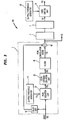
- Fig. 3 shows a block diagram of a device for limiting peaks of a signal according to the present invention.
- the device 100 includes a clipping threshold generator 10 for generating a clipping threshold signal V CL , a peak isolation unit 20 for receiving an input signal S(t) and generating a peak signal P(t) of the input signal S(t) based on the clipping threshold signal V CL , a local extrema isolation unit 30 for receiving the peak signal P(t) and generating an extrema signal E(t) based on the peak signal P(t), a filter 40 for filtering the extrema signal E(t) according to an appropriate impulse response of the filter 40 and generating a peak cancellation signal F(t), a delay unit 50 for delaying the input signal S(t) for a predetermined time period, and an adder 60 for combining the delayed input signal S(t) with the peak cancellation signal F(t) and generating an impulse clipped signal I(t) with a reduced P/A ratio and an improved spectrum response.
- V CL clip
- the clipping threshold generator 10, the peak isolation unit 20, the local extrema isolation unit 30, the filter 40, the delay unit 50, and the adder 60 constitute a single impulse clipping stage 1 of the invention.
- a hard limiting unit 70 may be optionally provided in the device 100 to hard limit the impulse clipped signal I(t) according to a threshold signal so as to prevent formation of small peaks in the impulse clipped signal I(t). These small peaks are rare in the impulse clipped signal I(t), but if present, the hard limiting unit 70 can easily remove the small peaks.
- Another clipping threshold generator 80 provides the threshold signal to the hard limiting unit 70.
- Figs. 4A-4E show examples of different signals output from the components of the device 100 shown in Fig. 3.
- the peak isolation unit 20 receives an input signal S(t), an example of which is shown in Fig. 4A. Based on a certain clipping threshold signal V CL , the peak isolation unit 20 isolates peaks of the input signal S(t) to generate a peak signal P(t), an example of which is shown in Fig. 4B.
- the local extrema isolation unit 30 receives the peak signal P(t) and further isolates the local extrema of the peak signal P(t) to generate an extrema signal E(t).
- the extrema signal E(t) resembles impulse signals, and an example of the extrema signal E(t) is shown in Fig. 4C.
- the filter 40 receives the extrema signal E(t) from the local extrema isolation unit 30 and filters it to generate a peak cancellation signal F(t), an example of which is shown in Fig. 4D.
- the adder 60 subtracts the peak cancellation signal F(t) from a delayed input signal S(t) to generate an impulse clipped signal I(t), an example of which is shown in Fig. 4E.
- I(t) S(t) - F(t).
- the clipping threshold generator 10 of Fig. 3 generates a clipping threshold signal V CL .
- the clipping threshold signal V CL is a certain voltage value at which the input signal S(t) is clipped. This value may be a fixed value stored in a memory of the clipping threshold generator 10, or can be a programmable parameter controlled by the clipping threshold generator 10 or other external devices.
- the clipping threshold generator 10 can be controlled by a CPU or other processors so that the clipping threshold signal V CL is varied according to predetermined conditions, for example, system load or system operation.
- the clipping threshold signal V CL embodying the clipping threshold value is output to the peak isolation unit 20.
- Fig. 5 shows an example of a logic circuit of the peak isolation unit 20 of Fig. 3.
- the peak isolation unit 20 includes a plurality of adders 21 and 22, a comparator 23, and a multiplexer 24.
- the first adder 21 adds the clipping threshold signal V CL and the input signal S(t), and outputs the addition result to a "1" input port of the multiplexer 24.
- the second adder 22 subtracts the clipping threshold signal V CL from the input signal S(t), and outputs the result to a "2" input port of the multiplexer 24.
- the multiplexer 24 includes the "2" input port, the "1" input port, and a grounded “0" input port.
- the comparator 23 of the peak isolation unit 20 receives the clipping threshold signal V CL and the input signal S(t) as THRESHOLD and IN inputs, respectively.
- the comparator 23 compares IN and THREHSOLD inputs to each other. If IN > THRESHOLD, then the comparator 23 generates a selection signal for selecting the "2" input port of the multiplexer 24. If IN ⁇ -THRESHOLD, then the comparator 23 generates a selection signal for selecting the "1" input port of the multiplexer 24. Otherwise, the comparator 23 generates a selection signal for selecting the "0" input port of the multiplexer 24. According to the selection signal from the comparator 23, the multiplexer 24 outputs one of the signals from the "2", “1", and “0” input ports to generate the peak signal P(t).
- the peak signal P(t) is input to the local extrema isolation unit 30 of Fig. 3.
- Fig. 6 shows an exemplary logic circuit of the local extrema isolation unit 30.
- the local extrema isolation unit 30 includes a plurality of delay elements 31 and 32, a plurality of comparators 33a-33c and 34a-34c coupled to the delay elements 31 and 32, a plurality of AND-gates 35 and 36 coupled to the comparators 33a-33c and 34a-34c, an OR-gate 37 coupled to the AND-gates 35 and 36, and a multiplexer 38 coupled to the first delay element 31 and the OR-gate 37.
- the first delay element 31 delays the peak signal P(t) input to the local extrema isolation unit 30 for a predetermined time period.
- the second delay element 31 further delays the signal delayed by the first delay element 32 for the predetermined time period.
- the first comparator 33a receives the output of the first delay element 31 and the peak signal P(t), determines whether the output of the first delay element 31 is greater than or equal to the peak signal P(t), and generates a high level signal if yes and a low level signal if no.
- the second comparator 33b compares the outputs of the first and second delay elements 31 and 32. If the output of the first delay element 31 is greater than or equal to the output of the second delay element 32, the second comparator 33b generates a high level signal.
- the second comparator 33b generates a low level signal to the first AND-gate 35.
- the third comparator 33c determines whether the output of the first delay element 31 is greater than zero, and generates a high level signal if yes, and a low level signal if no.
- the first AND-gate 35 ANDs the outputs of the first, second and third comparators 33a-33c to generate an output signal to the OR-gate 37.
- the comparators 33a-33c process positive-valued samples of the peak signal P(t) whereas the comparators 34a-34c process negative-valued samples of the peak signal P(t).
- the fourth comparator 34a determines whether or not the output of the first delay element 31 is less than or equal to the peak signal P(t), and generates a. high level signal if yes, and a low level signal if no.
- the fifth comparator 34b determines whether or not the output of the first delay element 31 is less than or equal to the output of the second delay element 32, and generates a high level signal if yes, and a low level signal if no.
- the sixth comparator 34c determines whether or not the current value of the peak signal P(t) is negative, and generates a high level signal if yes, and a low level signal if no.
- the outputs of the fourth, fifth, and sixth comparators 34a-34c are output to the second AND-gate 36.
- the outputs of the first and second AND-gates 35 and 36 are received by the OR-gate 37, and the OR-gate 37 generates either a high level signal or a low level signal according to the OR-gate logic. If the OR-gate 37 generates a high level signal to the multiplexer 38, the multiplexer 38 selects the output of the first delay element 31 as its output. If the OR-gate 37 generates a low level signal to the multiplexer 38, the multiplexer 38 selects the ground voltage as its output. Accordingly, the local extrema isolation unit 30 isolates the local extrema of the peak signal P(t) to generate the extrema signal E(t).
- the filter 40 of Fig. 3 convolves (filters) the extrema signal E(t) of the local extrema isolation unit 30 through a filter having a predetermined impulse response.
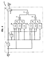
- Fig. 7A shows an example of the filter 40.
- the filter 40 includes a Finite Impulse Response (FIR) filter unit 41 which has a certain filtering characteristic.
- the FIR filter unit 41 provides an impulse response that constricts a majority of the filter's spectral energy to the band-pass region of the original input signal S(t).
- the FIR filter unit 41 can provide an impulse response, such as a window function including a Kaiser window, a Hamming window, a Hanning window, or any other impulse response that has the desired spectral characteristics of a low pass filter.
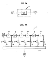
- Fig. 7B shows an exemplary logic circuit of the FIR filter unit 41 of Fig. 7A.
- the FIR filter unit 41 includes a plurality of delay elements 42a-42f connected to each other in series, a plurality of multipliers 44a-44g connected to the plurality of delay elements 44a-44f, and an adder 46 connected to the plurality of multipliers 44a-44g.
- the delay elements 42a-44f delay their input signal for the same delay time period.
- the multipliers 44a-44g multiply the extrema signal E(t) and the output of the delay elements 42a-42f with corresponding filter coefficients g0-g6.
- the first multiplier 44a multiplies the extrema signal E(t) input to the filter unit 41 with the first filter coefficient g0.
- the first delay element 42a delays the extrema signal E(t) by a predetermined delay time period, and outputs the delayed extrema signal E(t) to the second delay element 42b and the second multiplier 44b.
- the second multiplier 44b multiplies the delayed extrema signal E(t) with the second filter coefficient gl.
- the second, third, fourth, fifth and sixth delay elements 42b-42f further delay the delayed extrema signal E(t) by the predetermined delay time period, and output the delayed extrema signal E(t) to the third, fourth, fifth, sixth, and seventh multipliers 44c-44g, respectively.
- the multipliers 44c-44g multiply the delayed extrema signal E(t) with the third, fourth, fifth, sixth, and seventh coefficients g2-g6, respectively. Although six delay elements and seven multipliers have been shown and described, the filter unit 41 can include any number of delay elements and multipliers to provide a desired filter characteristic.
- the outputs of the multipliers 44a-44g are added by the adder 46, and the adder 46 outputs the addition result as the peak cancellation signal F(t).
- the delay unit 50 of Fig. 3 delays the input signal S(t) for a predetermined time period to compensate for the processing delay of the peak isolation unit 20, the local extrema isolation unit 30, and the filter 40.
- the delay unit 50 can be composed of a plurality of shift registers, or in digital memory, the data can be read out after a predetermined time period.
- the delay unit 50 can be implemented as a CCD delay, an RC delay, or other known delays in the art.
- the adder 60 of Fig. 3 adds the input signal S(t) delayed by the delay unit 50 and - (minus) peak cancellation signal F(t) generated by the filter 40.
- the adder 60 can subtract the peak cancellation signal F(t) of the filter 40 from the delayed input signal S(t).
- Such an adder or the like is known in the art.
- Fig. 8 shows an exemplary logic circuit of the hard limiting unit 70 of Fig. 3.
- the hard limiting unit 70 includes a comparator 71, an inverter 72, and a multiplexer 73.
- the inverter 72 inverts a clipping threshold signal V CL generated from a clipping threshold generator 80.
- the clipping threshold generator 80 may be the same as the clipping threshold generator 10, and the same clipping threshold signal V CL may be input to the peak isolation unit 20 and to the hard limiting unit 70.
- the comparator 71 receives the clipping threshold signal V CL and the impulse clipped signal I(t) as THRESHOLD and IN inputs, respectively.
- the comparator 71 determines whether or not IN is greater than or equal to THRESHOLD, and generates a selecting signal for selecting the "2" input port of the multiplexer 73 if yes. If IN is less than -THRESHOLD, then the comparator 71 generates a selection signal for selecting the "1" input port of the multiplexer 73. Otherwise, the comparator 71 generates a selection signal for selecting the "0" input port of the multiplexer 73.
- the multiplexer 73 receives the clipping threshold signal V CL , the output of the inverter 72, and the impulse clipped signal I(t) at its "2", “1", and “0” input ports, respectively. According to the selection signal from the comparator 71, one of the "2", “1", and “0” input ports of the multiplexer 73 is selected. Accordingly, a further peak-limited, impulse clipped signal I'(t) is generated.
- the impulse clipped signal I(t) or I'(t) of the present device 100 is a peak limited signal with a reduced P/A ratio, and is without significant out-of-band spectral artifacts.
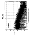
- Fig. 9 shows a graph for comparing the impulse clipped signal I(t) of the present invention with the hard clipped signal H(t) of the conventional art.
- the input signal S(t) is represented with a dash-dot line
- the hard clipped signal H(t) is represented with a solid line
- the impulse clipped signal I(t) (or I'(t)) is represented with a dashed line.
- the hard clipped signal H(t) depicts the input signal S(t) which has been hard-clipped according to the conventional hard clipping process.
- the impulse clipped signal I(t) depicts the input signal S(t) that has been peak-limited according to the impulse clipping operation of the present invention.
- the impulse clipped signal I(t) clearly has smoother peak edges than the hard clipped signal H(t), thereby reducing out-of-band spectral artifacts due to clipping.
- Fig. 10 shows an example of the peak cancellation signal F(t) of the present invention in comparison with a noise-like signal N(t) resulting from the conventional hard clipping process.
- the peak cancellation signal F(t) which is combined with the input signal S(t) in the present invention, has wider and smoother peaks than the noise-like signal N(t).
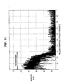
- Fig. 11 illustrates the spectrum of the peak cancellation signal F(t) showing a reduced spectrum emission outside of its pass-band region (about 0.3 frequency units).
- Fig. 12 shows the spectrum of the impulse clipped signal I(t) resulting from adding the input signal S(t) and the peak cancellation signal F(t) according to the present invention. It shows a significantly reduced spectrum emission outside of its pass-band region (about 0.3 frequency units), and a majority of the impulse clipped signal I(t) constrained within its pass-band region.
- the spectrum of the hard clipped signal H(t) of the conventional hard clipping process as shown in Fig. 2B, has a significantly high spectrum emission outside of its pass-band region.
- a clipping threshold signal V CL is generated by the clipping threshold generator 10 and input to the peak isolation unit 20.
- the peak isolation unit 20 isolates the peaks of an input signal S(t) as shown in Fig. 4A to generate a peak signal P(t) as shown in Fig. 4B.
- the local extrema of the peak signal P(t) are isolated by the local extrema isolation unit 30 to generate an extrema signal E(t) as shown in Fig. 4C.
- the extrema signal E(t) is filtered based on the impulse response of the filter 40 to generate a peak cancellation signal F(t) as shown in Fig. 4D.
- the peak cancellation signal F(t) is added with the delayed input signal S(t) to generate an impulse clipped signal I(t) as shown in Fig.
- the impulse clipped signal I(t) can be hard clipped by the hard limiting unit 70 to generate a further limited, impulse clipped signal I'(t).
- the impulse clipped signal I(t) or I'(t) has a reduced P/A ratio compared to the hard clipped signal of the conventional art, and has reduced out-of-band spectral artifacts compared to the window clipped signal of the conventional art.
- both analog and digital signals can be processed to limit their peaks without introducing intolerable levels of splatter, noise, or other characteristics which have been introduced in conventional methods.
Claims (12)
- Procédé de limitation des crêtes d'un signal, comprenant l'étape de :réception d'un signal d'entrée et d'un signal de référence ; caractérisé en ce qu'il comprend en outre les étapes de :fourniture d'un signal d'entrée retardé ;génération d'un signal d'extrema du signal d'entrée en se basant sur le signal de référence, le signal d'extrema correspondant à des crêtes du signal d'entrée ;filtrage du signal d'extrema selon une réponse de filtre prédéterminée pour générer un signal de filtre ; etcombinaison du signal de filtre et du signal d'entrée retardé pour générer un signal découpé par impulsion.
- Procédé selon la revendication 1, dans lequel ladite étape de fourniture comprend l'étape de :retardement du signal d'entrée par un intervalle de temps prédéterminé pour générer le signal d'entrée retardé.
- Procédé selon la revendication 1, dans lequel ladite étape de génération du signal d'extrema comprend l'étape :d'isolement des crêtes du signal d'entrée en sebasant sur le signal de référence pour générer un signal de crête.
- Procédé selon la revendication 3, dans lequel ladite étape d'isolement des crêtes comprend les étapes :d'addition du signal d'entrée et du signal de référence pour générer un premier signal totalisateur ;de soustraction du signal de référence du signal d'entrée pour générer un second signal totalisateur ;de comparaison du signal d'entrée au signal de référence et de génération d'un signal de sélection en se basant sur le résultat de comparaison ; etde sortie d'un parmi le premier signal totalisateur, le second signal totalisateur et d'un signal commun en se basant sur le signal de sélection.
- Procédé selon la revendication 3, dans lequel ladite étape de génération du signal d'extrema comprend en outre les étapes de :détection d'extrema locaux du signal de crête ; etgénération du signal d'extrema représentant les extrema locaux détectés du signal de crête.
- Procédé selon la revendication 5 dans lequel ladite étape de détection des extrema locaux comprend la comparaison du signal de crête avec des signaux de crête retardés.
- Procédé selon la revendication 3, dans lequel ladite étape de génération du signal d'extrema comprend en outre les étapes de :premier retardement du signal de crête pendant un intervalle de temps prédéterminé pour générer un premier signal de crête retardé ; etsecond retardement du premier signal de crête retardé pendant un intervalle de temps prédéterminé pour générer un second signal de crête retardé.
- Procédé selon la revendication 7, dans lequel ladite étape de génération du signal d'extrema comprend en outre l'étape de :comparaison du premier signal de crête retardé au signal de crête, du second signal de crête retardé au premier signal de crête retardé et du premier signal de crête retardé au signal de crête à une valeur de zéro.
- Procédé selon la revendication 8, dans lequel ladite étape de génération du signal d'extrema comprend en outre les étapes :d'intersection des sorties résultant de ladite étape de comparaison ;union des sorties résultant de ladite étape d'intersection ; etgénération d'un parmi le premier signal de crête retardé, le second signal de crête retardé et d'un signal commun en se basant sur une sortie résultant de ladite étape d'union.
- Procédé selon la revendication 1, comprenant en outre :des crêtes d'écrêtage d'un signal de sortie résultant de ladite étape de combinaison en se basant sur le signal de référence.
- Procédé selon la revendication 1, dans lequel dans ladite étape de combinaison, le signal de filtre est soustrait du signal d'entrée retardé.
- Appareil de limitation des crêtes d'un signal comprenant des moyens agencés pour exécuter chaque étape d'un procédé tel que revendiqué dans l'une quelconque des revendications précédentes.
Applications Claiming Priority (2)
| Application Number | Priority Date | Filing Date | Title |
|---|---|---|---|
| US126743 | 1987-11-30 | ||
| US09/126,743 US6356606B1 (en) | 1998-07-31 | 1998-07-31 | Device and method for limiting peaks of a signal |
Publications (3)
| Publication Number | Publication Date |
|---|---|
| EP0977355A2 EP0977355A2 (fr) | 2000-02-02 |
| EP0977355A3 EP0977355A3 (fr) | 2001-03-28 |
| EP0977355B1 true EP0977355B1 (fr) | 2005-09-21 |
Family
ID=22426446
Family Applications (1)
| Application Number | Title | Priority Date | Filing Date |
|---|---|---|---|
| EP99305709A Expired - Lifetime EP0977355B1 (fr) | 1998-07-31 | 1999-07-20 | Dispositif et méthode pour limiter les crêtes d'un signal |
Country Status (9)
| Country | Link |
|---|---|
| US (1) | US6356606B1 (fr) |
| EP (1) | EP0977355B1 (fr) |
| JP (1) | JP3484375B2 (fr) |
| KR (1) | KR20000012107A (fr) |
| CN (1) | CN1248096A (fr) |
| AU (1) | AU4234899A (fr) |
| BR (1) | BR9902933A (fr) |
| CA (1) | CA2273527A1 (fr) |
| DE (1) | DE69927328T2 (fr) |
Cited By (9)
| Publication number | Priority date | Publication date | Assignee | Title |
|---|---|---|---|---|
| US8463312B2 (en) | 2009-06-05 | 2013-06-11 | Mindspeed Technologies U.K., Limited | Method and device in a communication network |
| US8559998B2 (en) | 2007-11-05 | 2013-10-15 | Mindspeed Technologies U.K., Limited | Power control |
| US8712469B2 (en) | 2011-05-16 | 2014-04-29 | Mindspeed Technologies U.K., Limited | Accessing a base station |
| US8798630B2 (en) | 2009-10-05 | 2014-08-05 | Intel Corporation | Femtocell base station |
| US8849340B2 (en) | 2009-05-07 | 2014-09-30 | Intel Corporation | Methods and devices for reducing interference in an uplink |
| US8862076B2 (en) | 2009-06-05 | 2014-10-14 | Intel Corporation | Method and device in a communication network |
| US8904148B2 (en) | 2000-12-19 | 2014-12-02 | Intel Corporation | Processor architecture with switch matrices for transferring data along buses |
| US9042434B2 (en) | 2011-04-05 | 2015-05-26 | Intel Corporation | Filter |
| US9107136B2 (en) | 2010-08-16 | 2015-08-11 | Intel Corporation | Femtocell access control |
Families Citing this family (47)
| Publication number | Priority date | Publication date | Assignee | Title |
|---|---|---|---|---|
| US6104761A (en) * | 1998-08-28 | 2000-08-15 | Sicom, Inc. | Constrained-envelope digital-communications transmission system and method therefor |
| AU2466001A (en) * | 1999-12-30 | 2001-07-16 | Morphics Technology, Inc. | A configurable all-digital coherent demodulator system for spread spectrum applications |
| JP3478496B2 (ja) * | 2000-11-24 | 2003-12-15 | 松下電器産業株式会社 | 送信電力制御方法及びその装置並びに通信装置 |
| US7266354B2 (en) * | 2001-06-25 | 2007-09-04 | Telefonaktiebolaget Lm Ericsson (Publ) | Reducing the peak-to-average power ratio of a communication signal |
| US7170952B2 (en) | 2001-07-02 | 2007-01-30 | Powerwave Technologies, Inc. | System and method for post filtering peak power reduction in communications systems |
| US7095798B2 (en) | 2001-08-02 | 2006-08-22 | Powerwave Technologies, Inc. | System and method for post filtering peak power reduction in multi-carrier communications systems |
| FI20012059A0 (fi) | 2001-10-24 | 2001-10-24 | Nokia Corp | Menetelmä ja järjestely signaalin rajoittamiseksi radiolähettimessä |
| KR20030037108A (ko) * | 2001-11-02 | 2003-05-12 | 엘지전자 주식회사 | 이동통신 기지국 송신부의 피크 제거 장치 |
| US20030086507A1 (en) * | 2001-11-07 | 2003-05-08 | Jaehyeong Kim | Peak limiting architecture and method |
| WO2003075457A2 (fr) * | 2002-03-01 | 2003-09-12 | Andrew Corporation | Reduction du rapport de puissance de signal maximale-moyenne |
| GB0214729D0 (en) * | 2002-06-26 | 2002-08-07 | Koninkl Philips Electronics Nv | Digital receiver arrangement and related method |
| US6891902B2 (en) * | 2002-07-02 | 2005-05-10 | Intel Corporation | System and method for adjusting a power level of a transmission signal |
| US20040076247A1 (en) * | 2002-10-22 | 2004-04-22 | Wiseband Communications Ltd. | Peak-to-average power ratio modifier |
| WO2004051952A1 (fr) * | 2002-11-29 | 2004-06-17 | Telefonaktiebolaget Lm Ericsson (Publ) | Suppression de pic d'amplitude |
| US7260209B2 (en) * | 2003-03-27 | 2007-08-21 | Tellabs Operations, Inc. | Methods and apparatus for improving voice quality in an environment with noise |
| CN1538650B (zh) * | 2003-04-16 | 2010-04-07 | 华为技术有限公司 | 一种多载波信号削波装置及方法 |
| US7809150B2 (en) * | 2003-05-27 | 2010-10-05 | Starkey Laboratories, Inc. | Method and apparatus to reduce entrainment-related artifacts for hearing assistance systems |
| US7295816B2 (en) * | 2003-06-30 | 2007-11-13 | Crestcom, Inc. | Methods and apparatus for controlling signals |
| US7251463B2 (en) * | 2003-06-30 | 2007-07-31 | Crestcom, Inc. | Methods and apparatus for controlling signals |
| US7042287B2 (en) | 2003-07-23 | 2006-05-09 | Northrop Grumman Corporation | System and method for reducing dynamic range and improving linearity in an amplication system |
| JP2005106684A (ja) * | 2003-09-30 | 2005-04-21 | Konica Minolta Medical & Graphic Inc | 放射線画像変換パネル及びその製造方法 |
| US7187206B2 (en) * | 2003-10-30 | 2007-03-06 | International Business Machines Corporation | Power savings in serial link transmitters |
| FI20055012A0 (fi) * | 2005-01-07 | 2005-01-07 | Nokia Corp | Lähetyssignaalin leikkaaminen |
| US8553899B2 (en) * | 2006-03-13 | 2013-10-08 | Starkey Laboratories, Inc. | Output phase modulation entrainment containment for digital filters |
| US8116473B2 (en) | 2006-03-13 | 2012-02-14 | Starkey Laboratories, Inc. | Output phase modulation entrainment containment for digital filters |
| JP4750592B2 (ja) * | 2006-03-17 | 2011-08-17 | 富士通株式会社 | ピーク抑圧方法、ピーク抑圧装置、無線送信装置 |
| JP4878198B2 (ja) * | 2006-03-31 | 2012-02-15 | 日本無線株式会社 | 振幅制限装置 |
| US7783260B2 (en) * | 2006-04-27 | 2010-08-24 | Crestcom, Inc. | Method and apparatus for adaptively controlling signals |
| US8199948B2 (en) * | 2006-10-23 | 2012-06-12 | Starkey Laboratories, Inc. | Entrainment avoidance with pole stabilization |
| US8681999B2 (en) * | 2006-10-23 | 2014-03-25 | Starkey Laboratories, Inc. | Entrainment avoidance with an auto regressive filter |
| US8452034B2 (en) * | 2006-10-23 | 2013-05-28 | Starkey Laboratories, Inc. | Entrainment avoidance with a gradient adaptive lattice filter |
| WO2008051571A1 (fr) * | 2006-10-23 | 2008-05-02 | Starkey Laboratories, Inc. | Évitement de l'entrainement des filtres par algorithme de transformée du domaine de fréquence |
| EP1924044A1 (fr) * | 2006-11-16 | 2008-05-21 | Nokia Siemens Networks Gmbh & Co. Kg | Dispositif et procédé pour la génération d'un signal pour la réduction du PAR dans un système à multiporteuses |
| JP5098548B2 (ja) * | 2007-10-03 | 2012-12-12 | ヤマハ株式会社 | 増幅器 |
| CN101076008B (zh) * | 2007-07-17 | 2010-06-09 | 华为技术有限公司 | 信号的削波处理方法和设备 |
| US20090149152A1 (en) * | 2007-12-06 | 2009-06-11 | Motorola, Inc. | Method and device for maintaining average power of a baseband signal |
| CN101640559B (zh) * | 2008-07-31 | 2012-12-05 | 中兴通讯股份有限公司 | 一种降低数字中频信号峰均比的方法 |
| CN101834822B (zh) * | 2009-03-13 | 2012-10-10 | 电信科学技术研究院 | 一种基于峰值消除的峰值抵消方法和装置 |
| US8824574B2 (en) * | 2009-09-11 | 2014-09-02 | Crestcom, Inc. | Transmitting unit that reduces PAPR and method therefor |
| US8185065B2 (en) * | 2009-10-15 | 2012-05-22 | Crestcom, Inc. | Transmitting unit that reduces PAPR using out-of-band distortion and method therefor |
| KR101714784B1 (ko) * | 2010-01-25 | 2017-03-10 | 삼성전자주식회사 | 피크 윈도윙을 이용한 피크대평균전력비 감소 방법 및 장치 |
| US9654885B2 (en) | 2010-04-13 | 2017-05-16 | Starkey Laboratories, Inc. | Methods and apparatus for allocating feedback cancellation resources for hearing assistance devices |
| US8478325B2 (en) * | 2010-09-15 | 2013-07-02 | Telefonaktiebolaget L M Ericsson (Publ) | Low sample rate peak power reduction |
| GB2489716B (en) | 2011-04-05 | 2015-06-24 | Intel Corp | Multimode base system |
| US9848342B1 (en) | 2016-07-20 | 2017-12-19 | Ccip, Llc | Excursion compensation in multipath communication systems having performance requirements parameters |
| US11119063B2 (en) * | 2018-06-19 | 2021-09-14 | Samsung Electronics Co., Ltd. | Apparatus and method measuring bioimpedance and impedance |
| CN112968854B (zh) * | 2021-02-03 | 2022-03-29 | 青岛鼎信通讯股份有限公司 | 一种适用于中压载波系统的分段阈值削峰方法 |
Family Cites Families (11)
| Publication number | Priority date | Publication date | Assignee | Title |
|---|---|---|---|---|
| CH505510A (de) * | 1969-08-29 | 1971-03-31 | Patelhold Patentverwertung | Verfahren zur Mitübertragung der tiefen Signalfrequenzkomponenten eines Nachrichtensignals |
| US4208548A (en) * | 1977-07-19 | 1980-06-17 | Orban Associates, Inc. | Apparatus and method for peak-limiting audio frequency signals |
| US4295106A (en) * | 1979-10-04 | 1981-10-13 | Leonard Kahn | Method and means for introducing additional asymmetry into audio waves |
| US4667237A (en) * | 1982-05-12 | 1987-05-19 | Canon Kabushiki Kaisha | Image signal processing device |
| US4495643A (en) * | 1983-03-31 | 1985-01-22 | Orban Associates, Inc. | Audio peak limiter using Hilbert transforms |
| FI89846C (fi) | 1991-11-29 | 1993-11-25 | Nokia Mobile Phones Ltd | En deviationsbegraensare foer en fraon en radiotelefon utsaend signal |
| US5287387A (en) | 1992-03-06 | 1994-02-15 | Motorola, Inc. | Low splatter peak-to-average signal reduction |
| US5638403A (en) | 1995-04-28 | 1997-06-10 | Motorola, Inc. | Low-splatter peak-to-average signal reduction with interpolation |
| US5762068A (en) | 1995-11-27 | 1998-06-09 | Quinton Instrument Company | ECG filter and slew rate limiter for filtering an ECG signal |
| DE19548172A1 (de) | 1995-12-22 | 1996-05-23 | Michael Quaschnowitz | Verfahren zur verzerrungsarmen Amplitudenbegrenzung elektrischer Signale |
| US5737434A (en) * | 1996-08-26 | 1998-04-07 | Orban, Inc. | Multi-band audio compressor with look-ahead clipper |
-
1998
- 1998-07-31 US US09/126,743 patent/US6356606B1/en not_active Expired - Lifetime
-
1999
- 1999-06-03 CA CA002273527A patent/CA2273527A1/fr not_active Abandoned
- 1999-07-19 BR BR9902933-2A patent/BR9902933A/pt not_active Application Discontinuation
- 1999-07-20 EP EP99305709A patent/EP0977355B1/fr not_active Expired - Lifetime
- 1999-07-20 DE DE69927328T patent/DE69927328T2/de not_active Expired - Lifetime
- 1999-07-28 AU AU42348/99A patent/AU4234899A/en not_active Abandoned
- 1999-07-29 CN CN99110553A patent/CN1248096A/zh active Pending
- 1999-07-30 JP JP21606799A patent/JP3484375B2/ja not_active Expired - Fee Related
- 1999-07-30 KR KR1019990031344A patent/KR20000012107A/ko not_active Application Discontinuation
Cited By (10)
| Publication number | Priority date | Publication date | Assignee | Title |
|---|---|---|---|---|
| US8904148B2 (en) | 2000-12-19 | 2014-12-02 | Intel Corporation | Processor architecture with switch matrices for transferring data along buses |
| US8559998B2 (en) | 2007-11-05 | 2013-10-15 | Mindspeed Technologies U.K., Limited | Power control |
| US8849340B2 (en) | 2009-05-07 | 2014-09-30 | Intel Corporation | Methods and devices for reducing interference in an uplink |
| US8463312B2 (en) | 2009-06-05 | 2013-06-11 | Mindspeed Technologies U.K., Limited | Method and device in a communication network |
| US8862076B2 (en) | 2009-06-05 | 2014-10-14 | Intel Corporation | Method and device in a communication network |
| US8892154B2 (en) | 2009-06-05 | 2014-11-18 | Intel Corporation | Method and device in a communication network |
| US8798630B2 (en) | 2009-10-05 | 2014-08-05 | Intel Corporation | Femtocell base station |
| US9107136B2 (en) | 2010-08-16 | 2015-08-11 | Intel Corporation | Femtocell access control |
| US9042434B2 (en) | 2011-04-05 | 2015-05-26 | Intel Corporation | Filter |
| US8712469B2 (en) | 2011-05-16 | 2014-04-29 | Mindspeed Technologies U.K., Limited | Accessing a base station |
Also Published As
| Publication number | Publication date |
|---|---|
| EP0977355A3 (fr) | 2001-03-28 |
| BR9902933A (pt) | 2000-03-08 |
| US6356606B1 (en) | 2002-03-12 |
| KR20000012107A (ko) | 2000-02-25 |
| JP2000216654A (ja) | 2000-08-04 |
| CN1248096A (zh) | 2000-03-22 |
| EP0977355A2 (fr) | 2000-02-02 |
| JP3484375B2 (ja) | 2004-01-06 |
| DE69927328T2 (de) | 2006-06-14 |
| AU4234899A (en) | 2000-03-09 |
| DE69927328D1 (de) | 2005-10-27 |
| CA2273527A1 (fr) | 2000-01-31 |
Similar Documents
| Publication | Publication Date | Title |
|---|---|---|
| EP0977355B1 (fr) | Dispositif et méthode pour limiter les crêtes d'un signal | |
| EP1821474B1 (fr) | Appareil de suppression de pics de voltage d' un signal | |
| KR102175019B1 (ko) | 상쇄 펄스 파고율 저감 | |
| WO2003001697A2 (fr) | Reduction du rapport valeur de crete sur valeur moyenne de la puissance d'un signal de communication | |
| US20160028574A1 (en) | Device of crest factor reduction | |
| EP3175594B1 (fr) | Réduction de facteur de crête | |
| US7702175B2 (en) | Image processing apparatus for enhancing high frequency components | |
| US20060120479A1 (en) | System and method for crest factor reduction | |
| US7362819B2 (en) | Device and method for reducing peaks of a composite signal | |
| CN114500211B (zh) | 高精度多相cfr系统及方法 | |
| EP0834998A2 (fr) | Récepteur à spectre étalé avec élimination d'interférence à bande étroite | |
| US20100310007A1 (en) | Filter Device | |
| de Barcellos et al. | Optimization of FRM filters using the WLS–Chebyshev approach | |
| KR100782610B1 (ko) | 적응성 라인 인핸서 | |
| JP2626536B2 (ja) | リンギング除去装置 | |
| US6233022B1 (en) | Video signal enhancement through non-linear combination of left and right different signals | |
| US5495496A (en) | Method and apparatus for suppressing linear amplitude interference from bandspread communication signals | |
| US6844791B2 (en) | Digital pulse shaper with variable weighting function | |
| KR100195861B1 (ko) | 디지탈 로우 패스 필터 | |
| JP4745001B2 (ja) | ピーク抑圧装置および送信装置 | |
| Dolecek et al. | Computationally efficient FIR filter design based on impulse response rounding and sharpening | |
| JPH0770957B2 (ja) | Firフィルタ | |
| WO2002015396A1 (fr) | Conformateur d'impulsion numerique dote d'une fonction de pesee | |
| WO1997012482A1 (fr) | Traitement de signaux video |
Legal Events
| Date | Code | Title | Description |
|---|---|---|---|
| PUAI | Public reference made under article 153(3) epc to a published international application that has entered the european phase |
Free format text: ORIGINAL CODE: 0009012 |
|
| AK | Designated contracting states |
Kind code of ref document: A2 Designated state(s): DE FI FR GB SE |
|
| AX | Request for extension of the european patent |
Free format text: AL;LT;LV;MK;RO;SI |
|
| PUAL | Search report despatched |
Free format text: ORIGINAL CODE: 0009013 |
|
| AK | Designated contracting states |
Kind code of ref document: A3 Designated state(s): AT BE CH CY DE DK ES FI FR GB GR IE IT LI LU MC NL PT SE |
|
| AX | Request for extension of the european patent |
Free format text: AL;LT;LV;MK;RO;SI |
|
| 17P | Request for examination filed |
Effective date: 20010913 |
|
| AKX | Designation fees paid |
Free format text: DE FI FR GB SE |
|
| GRAP | Despatch of communication of intention to grant a patent |
Free format text: ORIGINAL CODE: EPIDOSNIGR1 |
|
| GRAS | Grant fee paid |
Free format text: ORIGINAL CODE: EPIDOSNIGR3 |
|
| GRAA | (expected) grant |
Free format text: ORIGINAL CODE: 0009210 |
|
| AK | Designated contracting states |
Kind code of ref document: B1 Designated state(s): DE FI FR GB SE |
|
| REG | Reference to a national code |
Ref country code: GB Ref legal event code: FG4D |
|
| RIN1 | Information on inventor provided before grant (corrected) |
Inventor name: HAHM, MARK DAVID |
|
| REF | Corresponds to: |
Ref document number: 69927328 Country of ref document: DE Date of ref document: 20051027 Kind code of ref document: P |
|
| PG25 | Lapsed in a contracting state [announced via postgrant information from national office to epo] |
Ref country code: SE Free format text: LAPSE BECAUSE OF FAILURE TO SUBMIT A TRANSLATION OF THE DESCRIPTION OR TO PAY THE FEE WITHIN THE PRESCRIBED TIME-LIMIT Effective date: 20051221 |
|
| ET | Fr: translation filed | ||
| PLBE | No opposition filed within time limit |
Free format text: ORIGINAL CODE: 0009261 |
|
| STAA | Information on the status of an ep patent application or granted ep patent |
Free format text: STATUS: NO OPPOSITION FILED WITHIN TIME LIMIT |
|
| 26N | No opposition filed |
Effective date: 20060622 |
|
| REG | Reference to a national code |
Ref country code: GB Ref legal event code: 732E Free format text: REGISTERED BETWEEN 20131121 AND 20131127 |
|
| REG | Reference to a national code |
Ref country code: FR Ref legal event code: CD Owner name: ALCATEL-LUCENT USA INC. Effective date: 20131122 |
|
| REG | Reference to a national code |
Ref country code: FR Ref legal event code: GC Effective date: 20140410 |
|
| REG | Reference to a national code |
Ref country code: FR Ref legal event code: RG Effective date: 20141015 |
|
| REG | Reference to a national code |
Ref country code: FR Ref legal event code: PLFP Year of fee payment: 17 |
|
| PGFP | Annual fee paid to national office [announced via postgrant information from national office to epo] |
Ref country code: FI Payment date: 20150713 Year of fee payment: 17 |
|
| REG | Reference to a national code |
Ref country code: FR Ref legal event code: PLFP Year of fee payment: 18 |
|
| PGFP | Annual fee paid to national office [announced via postgrant information from national office to epo] |
Ref country code: DE Payment date: 20160722 Year of fee payment: 18 Ref country code: GB Payment date: 20160721 Year of fee payment: 18 |
|
| PGFP | Annual fee paid to national office [announced via postgrant information from national office to epo] |
Ref country code: FR Payment date: 20160721 Year of fee payment: 18 |
|
| PG25 | Lapsed in a contracting state [announced via postgrant information from national office to epo] |
Ref country code: FI Free format text: LAPSE BECAUSE OF NON-PAYMENT OF DUE FEES Effective date: 20160720 |
|
| REG | Reference to a national code |
Ref country code: DE Ref legal event code: R119 Ref document number: 69927328 Country of ref document: DE |
|
| GBPC | Gb: european patent ceased through non-payment of renewal fee |
Effective date: 20170720 |
|
| REG | Reference to a national code |
Ref country code: FR Ref legal event code: ST Effective date: 20180330 |
|
| PG25 | Lapsed in a contracting state [announced via postgrant information from national office to epo] |
Ref country code: DE Free format text: LAPSE BECAUSE OF NON-PAYMENT OF DUE FEES Effective date: 20180201 Ref country code: GB Free format text: LAPSE BECAUSE OF NON-PAYMENT OF DUE FEES Effective date: 20170720 |
|
| PG25 | Lapsed in a contracting state [announced via postgrant information from national office to epo] |
Ref country code: FR Free format text: LAPSE BECAUSE OF NON-PAYMENT OF DUE FEES Effective date: 20170731 |
|
| REG | Reference to a national code |
Ref country code: DE Ref legal event code: R081 Ref document number: 69927328 Country of ref document: DE Owner name: WSOU INVESTMENTS, LLC, LOS ANGELES, US Free format text: FORMER OWNER: LUCENT TECHNOLOGIES INC., MURRAY HILL, N.J., US |