EP0977272A1 - Konstantstromgeber - Google Patents
Konstantstromgeber Download PDFInfo
- Publication number
- EP0977272A1 EP0977272A1 EP99410092A EP99410092A EP0977272A1 EP 0977272 A1 EP0977272 A1 EP 0977272A1 EP 99410092 A EP99410092 A EP 99410092A EP 99410092 A EP99410092 A EP 99410092A EP 0977272 A1 EP0977272 A1 EP 0977272A1
- Authority
- EP
- European Patent Office
- Prior art keywords
- type
- conductivity
- trigger
- current
- thyristor
- Prior art date
- Legal status (The legal status is an assumption and is not a legal conclusion. Google has not performed a legal analysis and makes no representation as to the accuracy of the status listed.)
- Withdrawn
Links
- 239000000758 substrate Substances 0.000 claims description 15
- 230000000694 effects Effects 0.000 claims description 3
- 239000004065 semiconductor Substances 0.000 claims description 2
- 238000001465 metallisation Methods 0.000 description 13
- 238000010586 diagram Methods 0.000 description 5
- XUIMIQQOPSSXEZ-UHFFFAOYSA-N Silicon Chemical compound [Si] XUIMIQQOPSSXEZ-UHFFFAOYSA-N 0.000 description 3
- 238000002955 isolation Methods 0.000 description 2
- 230000037452 priming Effects 0.000 description 2
- 229910052710 silicon Inorganic materials 0.000 description 2
- 239000010703 silicon Substances 0.000 description 2
- 241001080024 Telles Species 0.000 description 1
- 239000000969 carrier Substances 0.000 description 1
- 230000015556 catabolic process Effects 0.000 description 1
- 239000000470 constituent Substances 0.000 description 1
- 230000005684 electric field Effects 0.000 description 1
- 230000000977 initiatory effect Effects 0.000 description 1
- 238000004519 manufacturing process Methods 0.000 description 1
- 230000001052 transient effect Effects 0.000 description 1
Images
Classifications
-
- H—ELECTRICITY
- H01—ELECTRIC ELEMENTS
- H01L—SEMICONDUCTOR DEVICES NOT COVERED BY CLASS H10
- H01L29/00—Semiconductor devices specially adapted for rectifying, amplifying, oscillating or switching and having potential barriers; Capacitors or resistors having potential barriers, e.g. a PN-junction depletion layer or carrier concentration layer; Details of semiconductor bodies or of electrodes thereof ; Multistep manufacturing processes therefor
- H01L29/66—Types of semiconductor device ; Multistep manufacturing processes therefor
- H01L29/68—Types of semiconductor device ; Multistep manufacturing processes therefor controllable by only the electric current supplied, or only the electric potential applied, to an electrode which does not carry the current to be rectified, amplified or switched
- H01L29/70—Bipolar devices
- H01L29/74—Thyristor-type devices, e.g. having four-zone regenerative action
Definitions
- the present invention relates to generators or limiters current and more particularly current limiters capable of being inserted into power circuits to which high voltages can be applied, for example greater than a hundred volts.
- a current limiter is a component arranged in series in a circuit and intended to limit the current in the circuit at a constant value. So a current limiter is also often called a current generator.
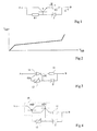
- FIG. 1 Another simple circuit for making a generator current is shown in figure 1.
- This circuit is connected between terminals A and B, terminal A being normally positive relative to terminal B, and includes the serial connection of a transistor T and a resistor R2.
- a resistor R1 is connected between base and collector of transistor T.
- a reference diode or avalanche diode Z is connected between the base of the transistor T and terminal B.
- the emitter current Ie, which flows in the resistance R2 is equal to (Vz-Vbe) / R2.
- the values Vz and Vbe being substantially constant, this current Ie is substantially constant.
- This circuit is however widely used and preferred to components of the source depletion MOS transistor type and grid interconnected because the limiting current can be easily fixed by external components (Vz, R1 ...), then that, in the case of the MOS transistor, the adjustment parameters are internal (channel resistance, threshold voltage, etc.).
- the present invention aims to achieve a generator of constant current which overcomes one or more of the disadvantages of each of the known current limiters.
- Another object of the present invention is to provide such a constant current generator which can be produced under form of monolithic component, possibly associated with other power components.
- this invention provides a constant current generator connected between first and second terminals, comprising a thyristor type openable by the trigger in series with a resistance; a current limiting component connected between the anode trigger and thyristor cathode trigger; and an voltage reference connected between the cathode and the trigger thyristor cathode.
- the voltage reference is an avalanche diode whose cathode is connected to the cathode of the opening thyristor by the trigger.
- the current limiting element is a resistor.
- the current limiting element is a saturable resistance.
- saturable resistance includes a box of a first type of conductivity comprising first and second zones of the second type of conductivity connected by a third area of the second type of conductivity at low doping level, the first zone of the second type of conductivity being connected to a heavily doped region of the first type of conductivity connected to the substrate, the box being brought to a first potential and the second zone of the second type of conductivity being connected to a second potential.
- the present invention relates to an embodiment of a generator current formed in an area of a semiconductor substrate of a first type of conductivity, comprising a first region of a second type of conductivity formed on the side of the rear face ; a first box of the second type of conductivity formed on the side of the upper face; a second region of the first type of conductivity formed in the first box; a second box of the second type of conductivity formed on the side of the face superior; a third region formed on the surface side upper in the second box; a band of the second type conductivity formed on the side of the upper face of the substrate.
- the vertical set of the first region, the substrate, the first caisson and the last region forms an opening thyristor by the trigger; the second caisson and the third region form an avalanche diode; a portion of the second box forms resistance; and said strip forms a second resistance.
- said band is a low doping band, hence it results that the second resistance is a saturable resistance to pinch effect.
- FIG. 3 represents the circuit of a generator current according to the present invention.
- This includes between terminals A and B a thyristor 10 of the type with opening by the trigger (GTO) with an anode trigger and a cathode trigger.
- This GTO thyristor is connected by its anode to terminal A and by its cathode at the first terminal of a resistor 11 whose second terminal is connected to terminal B.
- a limiting element current 12 is inserted between the anode trigger GA and the thyristor GK cathode trigger 10.
- An avalanche diode Z is connected by its cathode to the cathode trigger GK of the thyristor 10 and by its anode at terminal B.
- the current in resistor 11 or thyristor cathode current 10 is equal to (Vz-Vbe) / R, R being the value of resistance 11 and Vbe denoting the voltage drop between the cathode trigger and the thyristor cathode.
- R being the value of resistance 11 and Vbe denoting the voltage drop between the cathode trigger and the thyristor cathode.
- FIG 4 shows the same diagram as that of Figure 3 but in which the thyristor type openable by trigger 10 has been replaced by its diagram equivalent to two transistors.
- a GTO 10 corresponds to the association of two PNP and NPN transistors, the PNP transmitter corresponding to the anode A of the thyristor, the base of the PNP being connected to the NPN collector and corresponding to the trigger anode of the thyristor, the PNP collector being connected to the NPN base and corresponding to the cathode trigger and the emitter NPN corresponding to the thyristor cathode.
- thyristors and more particularly the thyristors open by the trigger (GTO) are used in switching mode, i.e. they are ordered to be either in a blocked state or in a fully conductive state, the intermediate state being only a transient state.
- GTO thyristors and more particularly the thyristors open by the trigger
- the product of current gains (Hfe) of the two transistors is less than 1.
- a current tends to flow from terminal A, through the emitter / base junction of the PNP transistor, of the resistor 12, of the base / emitter junction of the NPN transistor, and of the resistor 11, towards terminal B.
- the priming occurs because the gains PNP and NPN transistors increase as the current increases. This increase in current corresponds to a current of trigger.
- the system stabilizes at a product greater than 1. It self-maintains and the system remains conductive even if there is no more trigger current. However, the system tends to reblock when the earnings product which was greater than 1 tends to become less than 1.
- the initiation is caused by using simultaneously the anode trigger and the cathode trigger through the resistance 12, which makes it possible to solicit at the same time the PNP and NPN transistors.
- Vz more appreciably 0.7 volt corresponding to the base / emitter voltage of the NPN transistor
- the voltage is canceled across the transmitter base and brings in the system under regulation.
- a negative trigger current will get out of the NPN base.
- the thyristor being of the opening type by the trigger, its anode current, and therefore the current in the resistance 11, will tend to decrease.
- the voltage across the resistance 11, of value R therefore becomes less than Vz + 0.7 V and the cathode trigger current becomes positive again.
- the whole structure regulates the current up to a voltage limited by the voltage that can withstand its various elements, namely the GTO 10 thyristor, and the resistors 11 and 12.
- the resistors can be resistors high voltage and the GTO thyristor is naturally itself a high voltage component. With relatively components current regulation can be effective while the terminal voltage goes up to values of several hundred of volts, for example 600 volts or more.
- these architectures support tensions inverses of the same amplitude as the maximum forward voltage.
- the anode trigger junction of a thyristor can support conversely substantially the same voltage as the voltage reverse of the component, for example 600 volts. This is due, if we consider the diagram equivalent to the architecture of the transistor Classic PNP of a thyristor. Indeed, this PNP transistor is symmetrical and therefore supports the same reverse and direct voltage.
- a GTO thyristor adapted by example of letting currents of the order of the ampere pass, can be designed with a very high gain on closing (closing by trigger currents on the order of a tenth of a micro-amp), and be blocked by weak trigger currents (a few milliamps). We will therefore obtain a particular regulation satisfactory.
- the circuit according to the present invention illustrated in Figure 3, also compared to the conventional circuit of the figure 1 the advantage of being able to withstand high voltages both live and reverse, which in particular makes it possible to avoid associate it with a serial diode.
- a current limiting element 12 instead of a simple resistance a current limiting element such as a resistance saturable.
- This component will have a voltage / current such as that shown in Figure 5 having for example a value of the order of 75 ⁇ at zero voltage and a value limiting its current to an intensity of the order of a milliampere for high voltages, for example up to 600 volts.
- variable resistance can for example be produced in silicon as illustrated in FIG. 6.
- the component is formed in a substrate 20 type N including the rear side possibly overdoped is covered with a metallization M1 connected to the GA terminal.
- a metallization M1 connected to the GA terminal.
- two P-type regions are formed heavily doped 21 and 22 between which a region is formed P-type lightly doped 23.
- a region is formed 24 of heavily doped N type adjacent to region 22.
- the upper faces of the regions 22 and 24 are connected by a metallization M2 not connected to an external terminal.
- the upper face of the region 21 is in contact with a metallization M3 connected to the terminal GK. If a positive voltage is applied to the GA terminal with respect to the GK terminal, it can be considered that this voltage exists throughout the substrate region 20 and in the heavily doped N-type region 24, that is to say that metallization M2 is also at the positive potential of terminal GA. Thus, a current will flow from metallization M2 to metallization M3 in the weakly doped P-type layer 23. If the voltage between the terminals GA and GK increases, this current I will increase until the limit speed of the carriers is reached in the layer 23.
- the electric field at the junction between the substrate N and the lightly doped P-type region 23 will increase.
- the PN junction being a reverse junction will deplete and pinch the current in the region 23 which compensates for the increase in voltage which tends to occur.
- the configuration of the region 23 and an appropriate choice of its doping make it possible to adjust the pinch current Is (see FIG. 5).
- Those skilled in the art will be able to optimize these values.
- doping of the region 23 of 10 12 atoms / cm 2 redistributed over a depth of 5 to 10 ⁇ m with a length of the region 23 of the order of 100 ⁇ m makes it possible to hold more than 100 volts and to limit the current below 1 milliampere.
- FIG. 6 does not constitute that a possible embodiment of a current limiter used in place of resistor 12 in Figures 3 and 4. This embodiment has been described in detail because it can be used in a monolithic embodiment of the circuit of FIG. 3.
- FIG. 7 represents a monolithic embodiment of the component of FIG. 3 in the case where the current limiter 12 is of the type described previously in relation to FIG. 6.
- the structure is formed in an N-type substrate 30 the lower face of which carries a layer 31 of type P.
- the structure is surrounded by an isolation wall 32 of the type P.
- the part 30 of the substrate surrounded by the isolation wall 32 can be part of a larger component including other structures, for example other power components and possibly logical components.
- Thyristor 20 is made in vertical form. Its anode corresponds to the region P 31, its anode trigger to the N-type substrate 30, its trigger cathode with a box P 33 and its cathode with a region 34 of type N formed in box P 33.
- Another box of type P 36 is formed on the side of the upper face of the substrate 30 and contains an N 37 type region.
- region 21 is in fact formed of a part of the box 33.
- a metallization M11 which corresponds to the anode of the thyristor.
- Metallization M3 already described in relation to FIG. 6, is connected to an M12 metallization integral with region 37 of cathode of the avalanche diode Z.
- the metallization M13 corresponds to the terminal B which is connected to a first terminal of the resistor 11 and the metallization M14 corresponds to the second terminal of resistor 11 and extends to form the cathode metallization of the thyristor.
Landscapes
- Engineering & Computer Science (AREA)
- Microelectronics & Electronic Packaging (AREA)
- Power Engineering (AREA)
- Physics & Mathematics (AREA)
- Ceramic Engineering (AREA)
- Condensed Matter Physics & Semiconductors (AREA)
- General Physics & Mathematics (AREA)
- Computer Hardware Design (AREA)
- Thyristors (AREA)
Applications Claiming Priority (2)
| Application Number | Priority Date | Filing Date | Title |
|---|---|---|---|
| FR9809947A FR2781899B1 (fr) | 1998-07-30 | 1998-07-30 | Generateur de courant constant |
| FR9809947 | 1998-07-30 |
Publications (1)
| Publication Number | Publication Date |
|---|---|
| EP0977272A1 true EP0977272A1 (de) | 2000-02-02 |
Family
ID=9529345
Family Applications (1)
| Application Number | Title | Priority Date | Filing Date |
|---|---|---|---|
| EP99410092A Withdrawn EP0977272A1 (de) | 1998-07-30 | 1999-07-29 | Konstantstromgeber |
Country Status (3)
| Country | Link |
|---|---|
| US (1) | US7433166B1 (de) |
| EP (1) | EP0977272A1 (de) |
| FR (1) | FR2781899B1 (de) |
Cited By (1)
| Publication number | Priority date | Publication date | Assignee | Title |
|---|---|---|---|---|
| CN110597349A (zh) * | 2018-06-12 | 2019-12-20 | 恩智浦美国有限公司 | 具有可变电阻器电路的电流源 |
Families Citing this family (2)
| Publication number | Priority date | Publication date | Assignee | Title |
|---|---|---|---|---|
| DE102008044827B3 (de) * | 2008-08-28 | 2010-04-08 | Siemens Aktiengesellschaft | Verfahren und Vorrichtung zum Erzeugen einer zeitrasterangepassten Messsequenz für einen Magnetresonanz-Scanner, die auf einem Zeitraster des Magnetresonanz-Scanners ausführbar ist |
| US9653913B2 (en) * | 2015-02-17 | 2017-05-16 | Littelfuse, Inc. | Resistance change device providing overcurrent protection |
Citations (6)
| Publication number | Priority date | Publication date | Assignee | Title |
|---|---|---|---|---|
| JPH0360160A (ja) * | 1989-07-28 | 1991-03-15 | Toyo Electric Mfg Co Ltd | 自己消弧形サイリスタ |
| JPH06188410A (ja) * | 1992-10-21 | 1994-07-08 | Sanken Electric Co Ltd | 半導体装置 |
| JPH0778970A (ja) * | 1993-06-18 | 1995-03-20 | Sanken Electric Co Ltd | 半導体装置 |
| JPH07143733A (ja) * | 1993-11-16 | 1995-06-02 | Fuji Electric Co Ltd | スナバ回路 |
| EP0785577A1 (de) * | 1996-01-19 | 1997-07-23 | Sgs Thomson Microelectronics Sa | Telefonleitungs-Interface-Schutzbauelement |
| US5657195A (en) * | 1994-04-13 | 1997-08-12 | Sgs-Thomson Microelectronics S.A. | Overcurrent protection device |
Family Cites Families (16)
| Publication number | Priority date | Publication date | Assignee | Title |
|---|---|---|---|---|
| US3434038A (en) * | 1966-05-27 | 1969-03-18 | Carl W Vette | Dc current regulator |
| US4302687A (en) * | 1978-04-20 | 1981-11-24 | Nippon Electric Co., Ltd. | Semiconductor switch |
| FR2449369A1 (fr) * | 1979-02-13 | 1980-09-12 | Thomson Csf | Circuit logique comportant une resistance saturable |
| US4489340A (en) * | 1980-02-04 | 1984-12-18 | Nippon Telegraph & Telephone Public Corporation | PNPN Light sensitive semiconductor switch with phototransistor connected across inner base regions |
| JPS60187058A (ja) * | 1984-03-07 | 1985-09-24 | Hitachi Ltd | 半導体装置 |
| US5504449A (en) * | 1992-04-09 | 1996-04-02 | Harris Corporation | Power driver circuit |
| DE4303147C1 (de) * | 1993-01-30 | 1994-06-16 | Licentia Gmbh | GTO-Stromrichter mit quasi-resonantem Gleichspannungszwischenkreis |
| FR2727571A1 (fr) * | 1994-11-25 | 1996-05-31 | Sgs Thomson Microelectronics | Thyristor a sensibilite en retournement controlee |
| FR2745669B1 (fr) * | 1996-02-29 | 1998-05-22 | Sgs Thomson Microelectronics | Interrupteur statique monolithique a trois etats |
| FR2746998B1 (fr) * | 1996-03-26 | 1998-06-26 | Sgs Thomson Microelectronics | Protection contre les surtensions d'une interface de lignes telephoniques |
| US5663860A (en) * | 1996-06-28 | 1997-09-02 | Harris Corporation | High voltage protection circuits |
| FR2754392B1 (fr) * | 1996-10-04 | 1999-04-30 | Centre Nat Rech Scient | Thyristor dual normalement passant blocable par une impulsion appliquee sur la gachette |
| FR2770656B1 (fr) * | 1997-10-31 | 2000-01-14 | Sgs Thomson Microelectronics | Circuit de regulation de tension continue commutable |
| FR2782207B1 (fr) * | 1998-08-04 | 2000-11-03 | St Microelectronics Sa | Circuit de production d'arcs electriques |
| FR2782859B1 (fr) * | 1998-08-28 | 2000-11-17 | St Microelectronics Sa | Circuit de commutation |
| FR2809545B1 (fr) * | 2000-05-23 | 2002-10-11 | St Microelectronics Sa | Dispositif de protection serie pour une ligne de transmission de donnees ou d'energie |
-
1998
- 1998-07-30 FR FR9809947A patent/FR2781899B1/fr not_active Expired - Fee Related
-
1999
- 1999-07-29 EP EP99410092A patent/EP0977272A1/de not_active Withdrawn
- 1999-07-29 US US09/363,768 patent/US7433166B1/en not_active Expired - Fee Related
Patent Citations (6)
| Publication number | Priority date | Publication date | Assignee | Title |
|---|---|---|---|---|
| JPH0360160A (ja) * | 1989-07-28 | 1991-03-15 | Toyo Electric Mfg Co Ltd | 自己消弧形サイリスタ |
| JPH06188410A (ja) * | 1992-10-21 | 1994-07-08 | Sanken Electric Co Ltd | 半導体装置 |
| JPH0778970A (ja) * | 1993-06-18 | 1995-03-20 | Sanken Electric Co Ltd | 半導体装置 |
| JPH07143733A (ja) * | 1993-11-16 | 1995-06-02 | Fuji Electric Co Ltd | スナバ回路 |
| US5657195A (en) * | 1994-04-13 | 1997-08-12 | Sgs-Thomson Microelectronics S.A. | Overcurrent protection device |
| EP0785577A1 (de) * | 1996-01-19 | 1997-07-23 | Sgs Thomson Microelectronics Sa | Telefonleitungs-Interface-Schutzbauelement |
Cited By (1)
| Publication number | Priority date | Publication date | Assignee | Title |
|---|---|---|---|---|
| CN110597349A (zh) * | 2018-06-12 | 2019-12-20 | 恩智浦美国有限公司 | 具有可变电阻器电路的电流源 |
Also Published As
| Publication number | Publication date |
|---|---|
| FR2781899A1 (fr) | 2000-02-04 |
| US7433166B1 (en) | 2008-10-07 |
| FR2781899B1 (fr) | 2000-10-06 |
Similar Documents
| Publication | Publication Date | Title |
|---|---|---|
| EP0579561B1 (de) | Schutzschaltung gegen Überspannungen für Leistungsbauteil | |
| EP0714139B1 (de) | Zweipoliges Bauteil zur Überkopfzündung mit kontrollierter Empfindlichkeit | |
| EP0357528B1 (de) | MOS-Transistor und Anwendung bei einer Freilaufdiode | |
| EP0388329B1 (de) | Steuerschaltung für einen MOS-Leistungstransistor mit induktiver Last | |
| FR2533369A1 (fr) | Circuit de protection pour dispositifs a circuit integre et structure de semi-conducteur pour proteger un circuit integre | |
| FR2503456A1 (fr) | Dispositif de protection pour circuits integres | |
| EP0742591B1 (de) | Bauelement für den vollständigen Schutz einer Schnittstellenschaltung von Teilnehmerleitungen | |
| EP0780952B1 (de) | Monolithischer und statischer Strombegrenzer und Schutzschalter | |
| EP0359680B1 (de) | Integrierbare, aktive Diode | |
| FR3039014B1 (fr) | Protection de ligne telephonique contre les surtensions | |
| EP0872891A1 (de) | Bauteil zum Schnittstellenschutz von Telefonleitungen | |
| FR2572600A1 (fr) | Stabilisateur electronique de tension, utilisable en particulier dans l'automobile, avec protection contre les surtensions transitoires de polarite opposee a celle du generateur | |
| EP2348528A1 (de) | Schutzvorrichtung für einen integrierten Schaltkreis gegen elektrostatische Entladungen | |
| EP0977272A1 (de) | Konstantstromgeber | |
| FR2494040A1 (fr) | Dispositif a circuits integres a semiconducteurs proteges contre les surtensions accidentelles | |
| EP0742592A1 (de) | Empfindliches Schutzbauelement für Schnittstellenschaltung von Teilnehmerleitungen | |
| CH651160A5 (fr) | Amplificateur differentiel a transistors bipolaires realises en technologie cmos. | |
| FR2462025A1 (fr) | Circuit integre monolithique a transistors mos complementaires | |
| EP0881681B1 (de) | Anordnung zum Schützen einer integrierten MOS-Vorrichtung gegen Spannungsabfälle | |
| EP0820135B1 (de) | Statischer selbsthaltender Mikroschalter | |
| EP0704903A1 (de) | Halbleitervorrichtung zur Speisung, Rückleitung und Entmagnetisierung einer induktiven Last | |
| FR2745669A1 (fr) | Interrupteur statique monolithique a trois etats | |
| FR2738682A1 (fr) | Dispositif de protection contre des surtensions | |
| EP1290734B1 (de) | Anodenspannungssensor eines vertikalen leistungsbauelementes und verwendung zum schutz von kurzschlüssen | |
| EP1017103B1 (de) | Leistungsschalter mit DI/DT Regelung |
Legal Events
| Date | Code | Title | Description |
|---|---|---|---|
| PUAI | Public reference made under article 153(3) epc to a published international application that has entered the european phase |
Free format text: ORIGINAL CODE: 0009012 |
|
| AK | Designated contracting states |
Kind code of ref document: A1 Designated state(s): DE FR GB IT |
|
| AX | Request for extension of the european patent |
Free format text: AL;LT;LV;MK;RO;SI |
|
| 17P | Request for examination filed |
Effective date: 20000710 |
|
| AKX | Designation fees paid |
Free format text: DE FR GB IT |
|
| RAP1 | Party data changed (applicant data changed or rights of an application transferred) |
Owner name: STMICROELECTRONICS S.A. |
|
| 17Q | First examination report despatched |
Effective date: 20060726 |
|
| STAA | Information on the status of an ep patent application or granted ep patent |
Free format text: STATUS: THE APPLICATION IS DEEMED TO BE WITHDRAWN |
|
| 18D | Application deemed to be withdrawn |
Effective date: 20100202 |