EP0976173B1 - Mikrowellen-reflektorantenne - Google Patents
Mikrowellen-reflektorantenne Download PDFInfo
- Publication number
- EP0976173B1 EP0976173B1 EP99907317A EP99907317A EP0976173B1 EP 0976173 B1 EP0976173 B1 EP 0976173B1 EP 99907317 A EP99907317 A EP 99907317A EP 99907317 A EP99907317 A EP 99907317A EP 0976173 B1 EP0976173 B1 EP 0976173B1
- Authority
- EP
- European Patent Office
- Prior art keywords
- reflector
- antenna
- microwaves
- metallization
- subreflector
- Prior art date
- Legal status (The legal status is an assumption and is not a legal conclusion. Google has not performed a legal analysis and makes no representation as to the accuracy of the status listed.)
- Expired - Lifetime
Links
- 230000010287 polarization Effects 0.000 claims description 23
- 238000001465 metallisation Methods 0.000 claims description 20
- 230000005684 electric field Effects 0.000 claims description 15
- 230000010363 phase shift Effects 0.000 claims description 8
- 239000000758 substrate Substances 0.000 claims description 5
- 239000004020 conductor Substances 0.000 claims description 2
- 238000004519 manufacturing process Methods 0.000 description 8
- 238000010586 diagram Methods 0.000 description 6
- 238000000034 method Methods 0.000 description 5
- 238000004364 calculation method Methods 0.000 description 3
- 230000000737 periodic effect Effects 0.000 description 3
- 238000011161 development Methods 0.000 description 2
- 230000018109 developmental process Effects 0.000 description 2
- 239000003989 dielectric material Substances 0.000 description 2
- 238000009826 distribution Methods 0.000 description 2
- 230000001902 propagating effect Effects 0.000 description 2
- 238000004458 analytical method Methods 0.000 description 1
- 238000003491 array Methods 0.000 description 1
- 238000004590 computer program Methods 0.000 description 1
- 230000001934 delay Effects 0.000 description 1
- 238000005516 engineering process Methods 0.000 description 1
- 239000002184 metal Substances 0.000 description 1
- 238000005457 optimization Methods 0.000 description 1
- 238000007493 shaping process Methods 0.000 description 1
- 230000003595 spectral effect Effects 0.000 description 1
Images

Classifications
-
- H—ELECTRICITY
- H01—ELECTRIC ELEMENTS
- H01Q—ANTENNAS, i.e. RADIO AERIALS
- H01Q19/00—Combinations of primary active antenna elements and units with secondary devices, e.g. with quasi-optical devices, for giving the antenna a desired directional characteristic
- H01Q19/10—Combinations of primary active antenna elements and units with secondary devices, e.g. with quasi-optical devices, for giving the antenna a desired directional characteristic using reflecting surfaces
- H01Q19/18—Combinations of primary active antenna elements and units with secondary devices, e.g. with quasi-optical devices, for giving the antenna a desired directional characteristic using reflecting surfaces having two or more spaced reflecting surfaces
- H01Q19/185—Combinations of primary active antenna elements and units with secondary devices, e.g. with quasi-optical devices, for giving the antenna a desired directional characteristic using reflecting surfaces having two or more spaced reflecting surfaces wherein the surfaces are plane
-
- H—ELECTRICITY
- H01—ELECTRIC ELEMENTS
- H01Q—ANTENNAS, i.e. RADIO AERIALS
- H01Q15/00—Devices for reflection, refraction, diffraction or polarisation of waves radiated from an antenna, e.g. quasi-optical devices
- H01Q15/14—Reflecting surfaces; Equivalent structures
- H01Q15/22—Reflecting surfaces; Equivalent structures functioning also as polarisation filter
-
- H—ELECTRICITY
- H01—ELECTRIC ELEMENTS
- H01Q—ANTENNAS, i.e. RADIO AERIALS
- H01Q19/00—Combinations of primary active antenna elements and units with secondary devices, e.g. with quasi-optical devices, for giving the antenna a desired directional characteristic
- H01Q19/10—Combinations of primary active antenna elements and units with secondary devices, e.g. with quasi-optical devices, for giving the antenna a desired directional characteristic using reflecting surfaces
- H01Q19/18—Combinations of primary active antenna elements and units with secondary devices, e.g. with quasi-optical devices, for giving the antenna a desired directional characteristic using reflecting surfaces having two or more spaced reflecting surfaces
- H01Q19/19—Combinations of primary active antenna elements and units with secondary devices, e.g. with quasi-optical devices, for giving the antenna a desired directional characteristic using reflecting surfaces having two or more spaced reflecting surfaces comprising one main concave reflecting surface associated with an auxiliary reflecting surface
- H01Q19/195—Combinations of primary active antenna elements and units with secondary devices, e.g. with quasi-optical devices, for giving the antenna a desired directional characteristic using reflecting surfaces having two or more spaced reflecting surfaces comprising one main concave reflecting surface associated with an auxiliary reflecting surface wherein a reflecting surface acts also as a polarisation filter or a polarising device
-
- H—ELECTRICITY
- H01—ELECTRIC ELEMENTS
- H01Q—ANTENNAS, i.e. RADIO AERIALS
- H01Q3/00—Arrangements for changing or varying the orientation or the shape of the directional pattern of the waves radiated from an antenna or antenna system
- H01Q3/44—Arrangements for changing or varying the orientation or the shape of the directional pattern of the waves radiated from an antenna or antenna system varying the electric or magnetic characteristics of reflecting, refracting, or diffracting devices associated with the radiating element
- H01Q3/46—Active lenses or reflecting arrays
Definitions
- the invention relates to a polarized microwave reflector antenna having a primary radiator, a subreflector permeable to microwaves of a desired polarization, and a main reflector for collimated reflection of the microwaves with a polarization rotated in the desired direction according to the preamble of claim 1.
- a polarized microwave reflector antenna having a primary radiator, a subreflector permeable to microwaves of a desired polarization, and a main reflector for collimated reflection of the microwaves with a polarization rotated in the desired direction according to the preamble of claim 1.
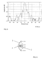
- FIG Fig. 6 An embodiment of a known antenna is shown in FIG Fig. 6 shown.
- the subreflector 2 has the property of a polarizing filter and is arranged to reflect waves of this polarization.
- the wave thus passes to the main reflector 3, where it is reflected again while being rotated in its polarization direction in such a way (twist reflector) that it can now pass unhindered through the sub-reflector 2.
- the field propagating from such an antenna is not obstructed by feeders, primary emitters, subreflectors or the like, as is the case with other reflector antennas which are not limited to one polarization direction.
- the bundling takes place in that the main reflector 3 for converting the spherical wave in a plane wave has a metallic reflector with a parabolic shape.
- bundling may be done according to WO 95/18980 Also done with a microwave lens, which is arranged in front of or behind the sub-reflector 2.
- microwave antennas of this type have several disadvantages.
- a parabolic reflector When a parabolic reflector is used for focusing, there is the difficulty of adapting the twist reflector to the parabolic shape without affecting the rotation of the polarization direction or the properties of the parabolic reflector.
- special requirements For the mechanical production of such an antenna special requirements must therefore be made in terms of accuracy and allowable tolerances, resulting in significant cost disadvantages.
- the invention is therefore an object of the invention to provide a microwave antenna for polarized microwaves, in which the cost of mechanical production is much lower, without having to be taken into account in view of the directional characteristics significant restrictions.
- a reflector antenna of the type mentioned which is characterized in that the primary radiator is arranged in the plane of the main reflector, wherein the dipoles have a predeterminable length and width, whereby between the reflected electric field components E yaus , E xaus parallel and perpendicular to the respective dipole axis, a phase shift of 180 ° is formed and at each dipole the phase of the reflected electric field E out relative to the phase of the incident electric field E in is shifted in such a way that the total field generated by all dipoles predetermined (eg ) Has wavefronts.
- the type of wavefronts specified depends on the requirements of the respective applications.
- antennas with PencilBeam characteristic are e.g. Antennas with fan beam or Cosecans characteristic possible or antennas with multiple lobes.
- a particular advantage of the solution with flat wavefronts is that the advantages of a folded reflector antenna with polarization rotation, namely a small depth of the antenna without limiting the maximum geometric aperture, with the advantages of planar manufacturing technology, which are primarily due to their much lower technical effort, are connected.
- the accuracy of the antenna or the characteristic of the antenna diagram is determined by the number and density of the dipoles.
- the focus of the effort required for the production is thus shifted from the mechanical manufacturing to the calculation of the individual dipoles.
- Such a calculation can be carried out with appropriate computer programs and thus does not cost so much in weight.
- photolitographic o. ⁇ . Method can be used with which even the smallest metallic structures can be produced in a known manner.
- the main reflector is formed, in particular, by a dielectric plate with a low loss factor, on which the dipoles in the form of a metallization structure are located on the side facing the incident microwaves, and a continuous metallization layer on the side facing away from the incident microwaves is applied.
- the metallization structures according to the invention have a rectangular shape, but they can e.g. have the shape of a cross or a disc.
- the subreflector according to the invention is a substrate with a metallization in the form of a polarization grating.
- the subreflector may additionally have metallization structures for beam shaping of the microwaves emanating from the primary radiator and / or the main reflector.
- the primary radiator may preferably be a horn antenna or a microstrip line antenna. It is also conceivable, however, any other antenna form that illuminates the reflector in a suitable manner.
- FIG. 1 embodiment of the invention shown has a primary radiator 1, which is directed to a sub-reflector 2.
- the subreflector 2 has the property of a polarization filter.
- the primary radiator 1 lies in the plane of a main reflector 3, which is arranged parallel to the sub-reflector 2 and has the property that it reflects the polarization plane of an incident wave rotated by 90 ° and also delays its phase in such a way that the reflected waves in total form even wavefronts.
- the antenna operates in such a way that the primary radiator 1 generates polarized waves which propagate spherically and strike the subreflector 2.
- the polarization plane of these waves and the forward direction of the subreflector 2 form an angle of 90 °, so that the waves are reflected and then fall on the main reflector 3.
- the main reflector 3 reflects the waves with a polarization plane rotated by 90 °, the re-reflected waves can now pass through the subreflector 2 and also have planar wavefronts (here in the example).
- the primary radiator 1 is a horn antenna known per se, but may alternatively be a microstrip line antenna. It is also conceivable, however, any other antenna form that illuminates the reflector in a suitable manner.
- the subreflector 2 is a polarizing filter in the form of a substrate 21 with corresponding metallization 22nd realized and is arranged relative to the polarization axis of the electric field of the primary radiator 1 so that this field is reflected.
- the main reflector 3 consists of a planar dielectric 31 with a low loss factor, which is provided on the rear side (ie on the side facing away from the incident microwaves) with a continuous metallic layer 32.
- On the front side of the dielectric 31 is an arrangement of individual metallization structures 33, which have a substantially rectangular basic shape, the dimensions of which, however, are very different depending on their location on the main reflector 3 (cf. FIG. 3 ).
- the structures 33 are aligned parallel to one another with their axis enclosing an angle of typically 45 ° with the polarization direction of the electric field.
- One of these metallization structures 33 is associated with the corresponding field components in FIG FIG. 2 shown.
- the incident electric field E can in parallel and a portion E xin be decomposed perpendicular to the axis of the metallization structure 33 in a portion E yin.
- the light reflected at the structure of field E is correspondingly from a content E and a content E Yau parallel xaus perpendicular to the axis of the structure 33 together.
- phase shift .DELTA. ⁇ is selected depending on the coordinates of the individual metallization on the main reflector in each case so that here in the example, the waves reflected at all structures have a total of a planar wavefront, ie are bundled.
- a first step for a plane wave incident on a periodic arrangement of these structures, all of which have a certain selected length and width, one first calculates the phases of the reflection factor for the polarization of the wave parallel and perpendicular to the axis of the structures.
- Several such datasets are determined for arrays of structures each having different lengths and widths.
- a structure at a particular location of the main reflector is given dimensions in which the corresponding measured arrangement of identical structures causes a phase shift of 180 ° between the two components E yaus and E x out of the reflected electric field ( FIG. that is to say, a rotation of the plane of polarization of the reflected electric field in relation to that of the incident electric field of 90 °) and, in addition, a phase shift ⁇ required for the bundling of the total wave.
- the computational determination of the relationship between the dimensions of the structures and the phase of the reflection factor can be done for example by means of a field-theoretical method.
- the spectral range method is particularly suitable for this purpose.
- In the air and in the dielectric development for the field strengths are set, whose coefficients can be determined by the boundary or continuity conditions on the metal or the dielectric surfaces.
- this is to the comments in " Numerical Techniques for Microwave and Millimeter-Wave Passive Structures "by Tatsuo Itho, John Wiley & Sons, 1989 , in particular pages 334 ff, referenced.
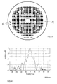
- the in Fig. 3 illustrated arrangement of metallization 33 on the planar dielectric 31.
- the arrangement according to the invention has a total of 364 rectangular structures whose centers form a grid with a mesh size of 6 x 6 mm.
- the dimensions of the structures vary according to the invention, depending on the above-described phase conditions in the range between 1 mm and 5.8 mm.
- a polarizing filter with conductor tracks with a width of 120 microns and a distance of 600 microns, which are located on a substrate with a height of 254 microns and a dielectric constant of 2.5.
- the sub-reflector has a distance of 45 mm from the main reflector.
- the diameter of the antenna is 150 mm.
- Fig. 4 shows for this antenna the measured far field diagram in the H plane, while in Fig. 5 represents the far field diagram in the E plane.
- the subreflector 2 may additionally have a beam-forming property. This can be achieved by obtaining the inner side of the polarization grating in a single-layered structure, or other metallization structures in the case of a multilayer structure. As a result, for example, an additional bundling is possible through which the focal length or the depth of the antenna is further reduced.
- the antenna is designed so that the main reflector has the property of generating wavefronts that lead to a far-field diagram that does not have the greatest gain, but e.g. has a so-called fan beam or a so-called Cosecans form or even several lobes as far field characteristic.
Landscapes
- Physics & Mathematics (AREA)
- Electromagnetism (AREA)
- Aerials With Secondary Devices (AREA)
Description
- Die Erfindung betrifft eine Reflektorantenne für polarisierte Mikrowellen mit einem Primärstrahler, einem für Mikrowellen einer gewünschten Polarisation durchlässigen Subreflektor und einem Hauptreflektor zur gebündelten Reflektion der Mikrowellen mit einer in die gewünschte Richtung gedrehten Polarisation gemäß dem Oberbegriff des Patentanspruchs 1. Eine solche Antenne ist bereits aus "Antenne Engineering Handbook"; 2nd Edition; Editors: R.C. Johnson, H.Jasik (McGraw-Hill, New York, 1961) Seiten 17-28 bis 17-30 bekannt. Aus Sikora J."FLAPS™ Reflector Antennas"; Atlanta, June 16-17,1993; Seiten 233-238 ist eine Antenne bekannt, bei welcher der Hauptreflektor außerdem eine Mehrzahl von in einer Ebene liegenden Dipolen mit zueinander parallele Achsen aufweist, die einen Winkel von 45° zu dem Vektor des einfallenden elektrischen Feldes aufweisen.
- Eine Ausführungsform einer bekannten Antenne ist in
Fig. 6 gezeigt. Mit dem im Bereich des Hauptreflektors 3 angeordneten und auf den Subreflektor 2 gerichteten Primärstrahler 1 wird eine sich kugelförmig ausbreitende Mikrowelle mit einer bestimmten Polarisation erzeugt. Der Subreflektor 2 hat die Eigenschaft eines Polarisationsfilters und ist so angeordnet, daß er Wellen mit dieser Polarisation reflektiert. Die Welle gelangt somit zu dem Hauptreflektor 3, an dem sie erneut reflektiert und dabei in ihrer Polarisationsrichtung in der Weise gedreht wird (Twistreflektor), daß sie nun ungehindert durch den Subreflektor 2 hindurchtreten kann. Das sich von einer solchen Antenne ausbreitende Feld wird nicht durch Speiseleitungen, Primärstrahler, Subreflektor oder ähnliches behindert, wie es bei anderen, nicht auf eine Polarisationsrichtung beschränkten Reflektorantennen der Fall ist. - Die Bündelung erfolgt dabei dadurch, daß der Hauptreflektor 3 zur Umwandlung der Kugelwelle in eine ebene Welle einen metallischen Reflektor mit einer parabolischen Form aufweist. Alternativ dazu kann die Bündelung gemäß der
WO 95/18980 - Mikrowellenantennen dieser Art haben jedoch verschiedene Nachteile. Wenn zur Bündelung ein parabolischer Reflektor verwendet wird, besteht die Schwierigkeit, den Twistreflektor an die parabolische Form anzupassen, ohne dadurch die Drehung der Polarisationsrichtung oder die Eigenschaften des Parabolreflektors zu beeinträchtigen. An die mechanische Fertigung einer solchen Antenne müssen deshalb im Hinblick auf die Genauigkeit und die zulässigen Toleranzen besondere Anforderungen gestellt werden, was zu erheblichen Kostennachteilen führt.
- Auch der Einsatz einer Mikrowellenlinse anstelle eines Parabolreflektors kann hier nur geringfügig Abhilfe schaffen, da auch die Fertigung von Linsen relativ aufwendig ist und diese gegenüber Reflektoren andere Nachteile aufweisen.
- Der Erfindung liegt deshalb die Aufgabe zugrunde, eine Mikrowellenantenne für polarisierte Mikrowellen zu schaffen, bei der der Aufwand für die mechanische Fertigung wesentlich geringer ist, ohne dass im Hinblick auf die Richtcharakteristik wesentliche Einschränkungen in Kauf genommen werden müssen.
- Die erfindungsgemäße Lösung dieser Aufgabe ist durch die Merkmale des Patentanspruchs 1 wiedergegeben. Die weiteren Ansprüche enthalten vorteilhafte Aus- und Weiterbildungen der Erfindung.
- Gelöst wird die Aufgabe mit einer Reflektorantenne der eingangs genannten Art, die sich dadurch auszeichnet, dass der Primärstrahler in der Ebene des Hauptreflektors angeordnet ist, wobei die Dipole eine vorgebbare Länge und Breite aufweisen, wodurch zwischen den reflektierten elektrischen Feldkomponenten Eyaus, Exaus parallel und senkrecht zu der jeweiligen Dipolachse eine Phasenverschiebung von 180° entsteht und an jedem Dipol die Phase des reflektierten elektrischen Feldes Eaus gegenüber der Phase des einfallenden elektrischen Feldes Ein in der Weise verschoben ist, dass das von allen Dipolen erzeugte Gesamtfeld vorgegebene (z.B. ebene) Wellenfronten aufweist.
- Die Art der vorgegebenen Wellenfronten richtet sich dabei nach den Erfordernissen der jeweiligen Anwendungen. Neben Antennen mit PencilBeam-Charakteristik sind z.B. Antennen mit Fan-Beam- oder Cosecans-Charakteristik möglich oder Antennen mit mehreren Keulen.
- Ein besonderer Vorteil der Lösung mit ebenen Wellenfronten besteht darin, dass die vorteile einer gefalteten Reflektor antenne mit Polarisationsdrehung, nämlich eine geringe Tiefe der Antenne ohne Einschränkung der maximalen geometrischen Apertur, mit den Vorteilen der planaren Herstellungstechnik, die in erster Linie in ihrem wesentlich geringeren technischen Aufwand liegen, verbunden werden.
- Die Genauigkeit der Antenne bzw. die Charakteristik des Antennendiagramms wird durch die Anzahl und Dichte der Dipole bestimmt. Der Schwerpunkt des zur Herstellung erforderlichen Aufwands wird somit von der mechanischen Fertigung auf die Berechnung der einzelnen Dipole verlagert. Eine solche Berechnung kann mit entsprechenden Rechnerprogrammen durchgeführt werden und fällt somit kostenmässig nicht so stark ins Gewicht. Zur mechanischen Fertigung können fotolitographische o. ä. Verfahren angewandt werden, mit denen in bekannter Weise auch kleinste metallische Strukturen erzeugt werden können.
- In der erfindungsgemäßen Reflektorantenne ist der Hauptreflektor insbesondere durch eine dielektrische Platte mit niedrigem Verlustfaktor gebildet, auf der sich auf der den einfallenden Mikrowellen zugewandten Seite die Dipole in Form von jeweils einer Metallisierungsstruktur befinden, und bei der auf der den einfallenden Mikrowellen abgewandten Seite eine durchgehende Metallisierungsschicht aufgebracht ist.
- Die Metallisierungsstrukturen haben erfindungsgemäß eine rechteckige Form, sie können jedoch z.B. die Form eines Kreuzes oder einer Scheibe aufweisen.
- Der Subreflektor ist erfindungsgemäß ein Substrat mit einer Metallisierung in Form eines Polarisationsgitters.
- Der Subreflektor kann zusätzlich Metallisierungsstrukturen zur Strahlformung der von dem Primärstrahler und/oder dem Hauptreflektor ausgehenden Mikrowellen aufweisen.
- Der Primärstrahler kann vorzugsweise eine Hornantenne oder eine Mikrostreifenleitungsantenne sein. Denkbar ist jedoch auch jede andere Antennenform, die den Reflektor in geeigneter Weise ausleuchtet.
- Weitere Einzelheiten, Merkmale und Vorteile der Erfindung ergeben sich aus der nachfolgenden Beschreibung einer bevorzugten Ausführungsform anhand der Zeichnungen.
- Es zeigen:
- FIG. 1
- einen schematischen Querschnitt durch eine bevorzugte Ausführungsform der erfindungsgemäßen Reflektorantenne
- FIG. 2
- eine Darstellung der elektrischen Feldkomponenten an einem einzelnen Dipol der Reflektorantenne gemäß
FIG. 1 - FIG. 3
- eine Draufsicht auf den Hauptreflektor der Reflektorantenne gemäß
FIG. 1 - FIG. 4
- ein Diagramm des Verlaufs der Feldstärke in der H-Ebene der Reflektorantenne gemäß
FIG. 1 - FIG. 5
- ein Diagramm des Verlaufs der Feldstärke in der E-Ebene der Reflektorantenne gemäß
FIG. 1 - FIG. 6
- eine bekannte Reflektorantenne für polarisierte Mikrowellen.
- Die in
Figur 1 gezeigte Ausführungsform der Erfindung weist einen Primärstrahler 1 auf, der auf einen Subreflektor 2 gerichtet ist. Der Subreflektor 2 hat die Eigenschaft eines Polarisationsfilters. Der Primärstrahler 1 liegt in der Ebene eines Hauptreflektors 3, der parallel zu dem Subreflektor 2 angeordnet ist und die Eigenschaft hat, daß er die Polarisationsebene einer einfallenden Welle um 90° gedreht reflektiert und außerdem ihre Phase in der Weise verzögert, daß die reflektierten Wellen insgesamt ebene Wellenfronten bilden. - Die Antenne arbeitet in der Weise, daß der Primärstrahler 1 polarisierte Wellen erzeugt, die sich kugelförmig ausbreiten und auf den Subreflektor 2 treffen. Die Polarisationsebene dieser Wellen und die Durchlaßrichtung des Subreflektors 2 bilden einen Winkel von 90°, so daß die Wellen reflektiert werden und anschließend auf den Hauptreflektor 3 fallen.
- Da der Hauptreflektor 3 die Wellen mit einer um 90° gedrehten Polarisationsebene reflektiert, können die erneut reflektierten Wellen nun durch den Subreflektor 2 hindurchtreten und weisen außerdem (hier im Beispiel) ebene Wellenfronten auf.
- Der Primärstrahler 1 ist eine an sich bekannte Hornantenne, kann aber alternativ hierzu auch eine Mikrostreifenleitungsantenne sein. Denkbar ist jedoch auch jede andere Antennenform, die den Reflektor in geeigneter Weise ausleuchtet.
- Der Subreflektor 2 ist als Polarisationsfilter in Form eines Substrates 21 mit entsprechender Metallisierung 22 realisiert und ist relativ zu der Polarisationsachse des elektrischen Feldes des Primärstrahlers 1 so angeordnet, daß dieses Feld reflektiert wird.
- Der Hauptreflektor 3 besteht aus einem planaren Dielektrikum 31 mit niedrigem Verlustfaktor, das auf der Rückseite (das heißt auf der den einfallenden Mikrowellen abgewandten Seite) mit einer durchgehenden metallischen Schicht 32 versehen ist. Auf der Vorderseite des Dielektrikums 31 befindet sich eine Anordnung von einzelnen Metallisierungsstrukturen 33, die eine im wesentlichen rechteckige Grundform aufweisen, deren Abmessungen jedoch in Abhängigkeit von ihrem Ort auf dem Hauptreflektor 3 sehr unterschiedlich sind (vgl. hierzu auch
FIG. 3 ). Die Strukturen 33 sind parallel zueinander ausgerichtet, wobei ihre Achse mit der Polarisationsrichtung des elektrischen Feldes einen Winkel von typischerweise 45° einschließt. - Eine dieser Metallisierungsstrukturen 33, die jeweils die Eigenschaft eines Dipols haben, ist mit den entsprechenden Feldkomponenten in
Figur 2 gezeigt. Das einfallende elektrische Feld E in kann in einen Anteil E yin parallel und einen Anteil E xin senkrecht zur Achse der Metallisierungsstruktur 33 zerlegt werden. Das an der Struktur reflektierte Feld E aus setzt sich entsprechend aus einem Anteil E yaus parallel und einem Anteil E xaus senkrecht zu der Achse der Struktur 33 zusammen. Durch geeignete Wahl der Länge und Breite der Struktur kann nun erreicht werden, daß die Anteile E yaus und E xaus einerseits eine Phasenverschiebung von 180° zueinander und andererseits eine zusätzliche gleiche Phasenverschiebung ΔØ gegenüber der einfallenden Welle Ein aufweisen. - Durch die Phasenverschiebung von 180° zwischen den Anteilen E yaus und E xaus an jeder Metallisierungsstruktur wird erreicht, daß die Polarisationsebene der reflektierten Welle um 90° gegenüber der Polarisationsebene der einfallenden Welle gedreht ist (vgl.
Figur 2 ). Die zusätzliche Phasenverschiebung ΔØ wird in Abhängigkeit von den Koordinaten der einzelnen Metallisierungsstruktur auf dem Hauptreflektor jeweils so gewählt, daß hier im Beispiel die an allen Strukturen reflektierten Wellen insgesamt eine ebene Wellenfront aufweisen, d.h. gebündelt sind. - Zur Vereinfachung der Dimensionierung der einzelnen Metallisierungsstrukturen geht man von einer periodischen Gesamtanordnung aus. In einem ersten Schritt errechnet man zunächst für eine ebene Welle, die auf eine periodische Anordnung dieser Strukturen einfällt, die alle eine bestimmte gewählte Länge und Breite aufweisen, die Phasen des Reflexionsfaktors für die Polarisation der Welle parallel sowie senkrecht zu der Achse der Strukturen. Es werden mehrere solche Datensätze für Anordnungen von Strukturen mit jeweils anderen Längen und Breiten ermittelt.
- Zu der Dimensionierung des Hauptreflektors erhält dann in einem zweiten Schritt eine Struktur an einem bestimmten Ort des Hauptreflektors diejenigen Abmessungen, bei denen die entsprechende gemessene Anordnung aus gleichen Strukturen eine Phasenverschiebung von 180° zwischen den beiden Komponenten E yaus und E xaus des reflektierten elektrischen Feldes (das heißt also eine Drehung der Polarisationsebene des reflektierten elektrischen Feldes gegenüber der des einfallenden elektrischen Feldes von 90°) und zusätzlich eine für die Bündelung der Gesamtwelle erforderliche Phasenverschiebung ΔØ zeigte.
- Die rechnerische Bestimmung des Zusammenhangs zwischen den Abmessungen der Strukturen und der Phase des Reflexionsfaktors kann zum Beispiel mit Hilfe eines feldtheoretischen Verfahrens erfolgen. Hierfür eignet sich besonders das Spektralbereichsverfahren. In der Luft und im Dielektrikum werden Entwicklungen für die Feldstärken angesetzt, deren Koeffizienten durch die Rand- bzw. Stetigkeitsbedingungen auf den Metall- bzw. den dielektrischen Oberflächen ermittelt werden können. Im einzelnen sei hierzu auf die Ausführungen in "Numerical Techniques for Microwave and Millimeter-Wave Passive Structures" von Tatsuo Itho, John Wiley & Sons, 1989, insbesondere die Seiten 334 ff, verwiesen.
- Da eine periodische Anordnung der Strukturen nur eine Annäherung an die tatsächlichen Verhältnisse darstellt, kann eine Optimierung durch eine Berechnung der Gesamtanordnung erfolgen.
- Für regelmäßige Strukturen aus Rechtecken, Kreuzen, Scheiben und ähnlichem können Ganzbereichsfunktionen für die Entwicklung der unbekannten Stromdichteverteilungen in bekannten Basisfunktionen verwendet werden. Mit Hilfe des an sich bekannten Galerkinverfahrens (vgl. z.B. den zuvor genannten Artikel von T. Itho et al.) können dann die Koeffizienten der Basisfunktionen bestimmt werden. Durch eine Überlagerung der Felder, die durch die berechneten Stromdichteverteilungen erregt werden, mit den Feldern, die durch Streuung der einfallenden Wellen an den Dielektrika errechnet werden, lassen sich präzise Aussagen über das Streuverhalten der Anordnung aus metallischen Strukturen und Dielektrika machen. Aus der Kenntnis des Zusammenhangs zwischen den geometrischen Abmessungen und dem daraus folgenden Streuverhalten lassen sich dann Designregeln für die Herstellung des Hauptreflektors ermittelt. Hierzu wird auf die Ausführungen in "Proceedings of APMC I; Seiten 225 bis 227 vom Dezember 1997 mit dem Titel "Full Wave Analysis of a Planar Reflektor Antenna" von D. Pilz und W. Menzel verwiesen.
- Für eine erfindungsgemäß realisierte Antenne mit einer Mittenfrequenz von 20 GHz ergibt sich die in
Fig. 3 dargestellte Anordnung von Metallisierungsstrukturen 33 auf dem planaren Dielektrikum 31. Die Anordnung weist erfindungsgemäß insgesamt 364 rechteckige Strukturen auf, deren Mittelpunkte ein Gitter mit einer Maschenweite von 6 x 6 mm bilden. Die Abmessungen der Strukturen variieren erfindungsgemäß in Abhängigkeit von den oben erläuterten Phasenbedingungen im Bereich zwischen 1 mm und 5,8 mm. - Gemäß der Erfindung dient als Subreflektor für diese Antenne ein Polarisationsfilter mit Leiterbahnen mit einer Breite von 120 µm und einem Abstand von 600 µm, die sich auf einem Substrat mit einer Höhe von 254 µm und einer Dielektrizitätszahl von 2,5 befinden. Der Subreflektor hat dabei einen Abstand von 45 mm von dem Hauptreflektor. Der Durchmesser der Antenne beträgt 150 mm.
-
Fig. 4 zeigt für diese Antenne das gemessene Fernfelddiagramm in der H-Ebene, während inFig. 5 das Fernfelddiagramm in der E-Ebene darstellt ist. - Bei einer anderen Ausführungsform der Erfindung kann der Subreflektor 2 zusätzlich eine strahlformende Eigenschaft haben. Dies kann dadurch erreicht werden, dass bei einer einschichtigen Struktur die Innenseite des Polarisationsgitters, oder bei einer mehrschichtigen Struktur andere Lagen weitere Metallisierungsstrukturen erhalten. Dadurch ist zum Beispiel eine zusätzliche Bündelung möglich, durch die die Brennweite bzw. die Tiefe der Antenne weiter vermindert wird.
- Ferner ist denkbar, daß die Antenne so gestaltet wird, daß der Hauptreflektor die Eigenschaft besitzt, Wellenfronten zu erzeugen, die zu einem Fernfelddiagramm führen, das nicht den größten Gewinn besitzt, sondern z.B. als Fernfeldcharakteristik einen sogenannten Fan-Beam oder eine sogenannte Cosecans-Form oder auch mehrere Keulen besitzt.
Claims (4)
- Reflektorantenne für polarisierte Mikrowellen mit einem Primärstrahler (1), einem für Mikrowellen einer gewünschten Polarisation durchlässigen Subreflektor (2) und einem Hauptreflektor (3) zur gebündelten Reflektion der Mikrowellen mit einer in die gewünschte Richtung gedrehten Polarisation, wobei der Hauptreflektor (3) eine Mehrzahl von in einer Ebene liegenden Dipolen (33) mit zueinander parallele Achsen aufweist, die einen Winkel von 45° zu dem Vektor des einfallenden elektrischen Feldes aufweisen,
wobei der Primärstrahler (1) in der Ebene des Hauptreflektors (3) angeordnet ist und dass die Dipole (33) eine vorgegebene Länge und Breite aufweisen, wodurch zwischen den reflektierten elektrischen Feldkomponenten Eyaus, Exaus parallel und senkrecht zu der jeweiligen Dipolachse eine Phasenverschiebung von 180° entsteht und an jedem Dipol (33) die Phase des reflektierten elektrischen Feldes Eaus gegenüber der Phase des einfallenden elektrischen Feldes Ein in der Weise verschoben ist, dass das von allen Dipolen (33) erzeugte Gesamtfeld vorgegebene Wellenfronten aufweist,
wobei die vorgegebenen Wellenfronten ebene Wellenfronten sind,
wobei der Hauptreflektor (3) eine dielektrische Platte (31) mit niedrigem Verlustfaktor aufweist, auf der sich auf der den einfallenden Mikrowellen zugewandten Seite die Dipole in Form von jeweils einer Metallisierungsstruktur (33) befinden und bei der auf der den einfallenden Mikrowellen abgewandten Seite eine durchgehende Metallisierungsschicht (32) aufgebracht ist,
wobei die Metallisierungsstrukturen (33) jeweils eine rechteckige Form aufweisen und wobei der Subreflektor (2) ein Substrat mit einer Metallisierung In Form eines Polarisationsgitters (21) ist,
dadurch gekennzeichnet, dass,
insbesondere für eine Mittenfrequenz von 20 GHz, der Hauptreflektor 364 rechteckige Metallisierungsstrukturen aufweist, deren Mittelpunkte ein Gitter mit einer Maschenweite von 6 x 6 mm bilden und dass der Subreflektor Leiterbahnen mit einer Breite von 120 µm und einem Abstand von 600 µm auf einem Substrat mit einer Dicke von 254 µm und einer Dielektrizitätszahl von 2,5 aufweist,
wobei die Abmessungen der Metallisierungsstrukturen (33) in Abhängigkeit von den oben erläuterten Phasenbedingungen im Bereich zwischen 1 mm und 5,8 mm variieren. - Reflektorantenne nach Anspruch 1, dadurch gekennzeichnet, dass der Primärstrahler (1) eine Homantenne ist.
- Reflektorantenne nach einem der Ansprüche 1, dadurch gekennzeichnet, dass der Primärstrahler (1) eine Mikrostreifenleitungsantenne ist.
- Reflektorantenne nach einem der vorangehenden Ansprüche, dadurch gekennzeichnet, dass der Durchmesser der Antenne 150 mm und der Abstand zwischen dem Hauptreflektor und dem Subreflektor 45 mm beträgt.
Applications Claiming Priority (5)
| Application Number | Priority Date | Filing Date | Title |
|---|---|---|---|
| DE19806887 | 1998-02-19 | ||
| DE19806887 | 1998-02-19 | ||
| DE19848722A DE19848722B4 (de) | 1998-02-19 | 1998-10-22 | Mikrowellen-Reflektorantenne |
| DE19848722 | 1998-10-22 | ||
| PCT/DE1999/000354 WO1999043049A1 (de) | 1998-02-19 | 1999-02-10 | Mikrowellen-reflektorantenne |
Publications (2)
| Publication Number | Publication Date |
|---|---|
| EP0976173A1 EP0976173A1 (de) | 2000-02-02 |
| EP0976173B1 true EP0976173B1 (de) | 2012-09-26 |
Family
ID=26043971
Family Applications (1)
| Application Number | Title | Priority Date | Filing Date |
|---|---|---|---|
| EP99907317A Expired - Lifetime EP0976173B1 (de) | 1998-02-19 | 1999-02-10 | Mikrowellen-reflektorantenne |
Country Status (2)
| Country | Link |
|---|---|
| EP (1) | EP0976173B1 (de) |
| WO (1) | WO1999043049A1 (de) |
Families Citing this family (4)
| Publication number | Priority date | Publication date | Assignee | Title |
|---|---|---|---|---|
| DE102004049626A1 (de) * | 2004-10-11 | 2006-04-13 | A.D.C. Automotive Distance Control Systems Gmbh | Radarantennenanordnung |
| CN104466429A (zh) * | 2013-11-08 | 2015-03-25 | 北京东方安高微电子科技有限公司 | 一种毫米波一维单脉冲双平面反射天线 |
| EP3531508B1 (de) * | 2016-11-30 | 2022-01-05 | Huawei Technologies Co., Ltd. | Reflektierende antennengruppe und kommunikationsvorrichtung |
| DE102019200411A1 (de) | 2019-01-16 | 2020-07-16 | Zf Friedrichshafen Ag | Verkehrsfahrzeug |
Family Cites Families (2)
| Publication number | Priority date | Publication date | Assignee | Title |
|---|---|---|---|---|
| US4905014A (en) * | 1988-04-05 | 1990-02-27 | Malibu Research Associates, Inc. | Microwave phasing structures for electromagnetically emulating reflective surfaces and focusing elements of selected geometry |
| US5455589A (en) * | 1994-01-07 | 1995-10-03 | Millitech Corporation | Compact microwave and millimeter wave radar |
-
1999
- 1999-02-10 WO PCT/DE1999/000354 patent/WO1999043049A1/de not_active Ceased
- 1999-02-10 EP EP99907317A patent/EP0976173B1/de not_active Expired - Lifetime
Also Published As
| Publication number | Publication date |
|---|---|
| WO1999043049A1 (de) | 1999-08-26 |
| EP0976173A1 (de) | 2000-02-02 |
Similar Documents
| Publication | Publication Date | Title |
|---|---|---|
| DE68910677T2 (de) | Mikrostreifenantenne. | |
| DE69612779T2 (de) | Antennensystem mit gesteuerter Ablenkung | |
| DE69013839T2 (de) | Zwei dielektrische Anpassungsschichten aufweisende Struktur für Radome und Linsen für grosse Einfallswinkel. | |
| DE69602052T2 (de) | Phasengesteuerte Gruppenantenne für Mehrbandbetrieb unter wechselseitiger Verwendung von Strahlern aus Hohlleitern und sich verjüngten Elementen | |
| DE69111757T2 (de) | Flache Mikrowellen-Schlitzantenne. | |
| DE19600609B4 (de) | Polarisator zur Umwandlung von einer linear polarisierten Welle in eine zirkular polarisierte Welle oder in eine linear polarisierte Welle mit gedrehter Polarisation und umgekehrt | |
| EP2622366B1 (de) | Antennensystem für radarsensoren | |
| DE112017001941T5 (de) | Antennenapparat | |
| DE69316962T2 (de) | Hohlleiter-Mikrostreifenleiterübergang | |
| DE60014594T2 (de) | Doppelspiralige Schlitzantenne für Zirkulare Polarisation | |
| DE4010101A1 (de) | Flachantenne | |
| DE69833070T2 (de) | Gruppenantennen mit grosser Bandbreite | |
| DE2821781A1 (de) | Hochfrequenzantenne | |
| DE69314412T2 (de) | Antenne mit Nebenkeulenunterdrückung | |
| DE3524503A1 (de) | Ebene mikrowellenantenne | |
| DE68917548T2 (de) | Koaxialer Wellenleiterphasenschieber. | |
| DE202022102307U1 (de) | Mehrbandantenne | |
| DE2810483C2 (de) | Antenne mit einem Schlitze aufweisenden Speisehohlleiter und einer mit diesem einen Winkel einschließenden Strahlerzeile | |
| DE19848722B4 (de) | Mikrowellen-Reflektorantenne | |
| EP0956615A1 (de) | Transmissions-polarisator | |
| DE4014133A1 (de) | Planarantenne | |
| DE19600516A1 (de) | Antenne | |
| EP0976173A1 (de) | Mikrowellen-reflektorantenne | |
| DE69408303T2 (de) | Antennensystem | |
| EP1006608B1 (de) | Mehrlagige Antennenanordnung |
Legal Events
| Date | Code | Title | Description |
|---|---|---|---|
| PUAI | Public reference made under article 153(3) epc to a published international application that has entered the european phase |
Free format text: ORIGINAL CODE: 0009012 |
|
| 17P | Request for examination filed |
Effective date: 19991026 |
|
| AK | Designated contracting states |
Kind code of ref document: A1 Designated state(s): AT BE CH DE DK ES FI FR GB IT LI NL SE |
|
| RAP1 | Party data changed (applicant data changed or rights of an application transferred) |
Owner name: EADS DEUTSCHLAND GMBH |
|
| 17Q | First examination report despatched |
Effective date: 20061116 |
|
| GRAP | Despatch of communication of intention to grant a patent |
Free format text: ORIGINAL CODE: EPIDOSNIGR1 |
|
| GRAS | Grant fee paid |
Free format text: ORIGINAL CODE: EPIDOSNIGR3 |
|
| GRAA | (expected) grant |
Free format text: ORIGINAL CODE: 0009210 |
|
| AK | Designated contracting states |
Kind code of ref document: B1 Designated state(s): AT BE CH DE DK ES FI FR GB IT LI NL SE |
|
| REG | Reference to a national code |
Ref country code: GB Ref legal event code: FG4D Free format text: NOT ENGLISH |
|
| REG | Reference to a national code |
Ref country code: CH Ref legal event code: EP |
|
| REG | Reference to a national code |
Ref country code: AT Ref legal event code: REF Ref document number: 577396 Country of ref document: AT Kind code of ref document: T Effective date: 20121015 |
|
| REG | Reference to a national code |
Ref country code: DE Ref legal event code: R096 Ref document number: 59915356 Country of ref document: DE Effective date: 20121129 |
|
| REG | Reference to a national code |
Ref country code: SE Ref legal event code: TRGR |
|
| REG | Reference to a national code |
Ref country code: NL Ref legal event code: T3 |
|
| REG | Reference to a national code |
Ref country code: ES Ref legal event code: FG2A Ref document number: 2393666 Country of ref document: ES Kind code of ref document: T3 Effective date: 20121227 |
|
| PG25 | Lapsed in a contracting state [announced via postgrant information from national office to epo] |
Ref country code: FI Free format text: LAPSE BECAUSE OF FAILURE TO SUBMIT A TRANSLATION OF THE DESCRIPTION OR TO PAY THE FEE WITHIN THE PRESCRIBED TIME-LIMIT Effective date: 20120926 |
|
| PGFP | Annual fee paid to national office [announced via postgrant information from national office to epo] |
Ref country code: ES Payment date: 20130227 Year of fee payment: 15 Ref country code: SE Payment date: 20130219 Year of fee payment: 15 |
|
| PGFP | Annual fee paid to national office [announced via postgrant information from national office to epo] |
Ref country code: NL Payment date: 20130219 Year of fee payment: 15 |
|
| PG25 | Lapsed in a contracting state [announced via postgrant information from national office to epo] |
Ref country code: DK Free format text: LAPSE BECAUSE OF FAILURE TO SUBMIT A TRANSLATION OF THE DESCRIPTION OR TO PAY THE FEE WITHIN THE PRESCRIBED TIME-LIMIT Effective date: 20120926 |
|
| PLBE | No opposition filed within time limit |
Free format text: ORIGINAL CODE: 0009261 |
|
| STAA | Information on the status of an ep patent application or granted ep patent |
Free format text: STATUS: NO OPPOSITION FILED WITHIN TIME LIMIT |
|
| BERE | Be: lapsed |
Owner name: EADS DEUTSCHLAND G.M.B.H. Effective date: 20130228 |
|
| 26N | No opposition filed |
Effective date: 20130627 |
|
| REG | Reference to a national code |
Ref country code: CH Ref legal event code: PL |
|
| REG | Reference to a national code |
Ref country code: DE Ref legal event code: R097 Ref document number: 59915356 Country of ref document: DE Effective date: 20130627 |
|
| PG25 | Lapsed in a contracting state [announced via postgrant information from national office to epo] |
Ref country code: LI Free format text: LAPSE BECAUSE OF NON-PAYMENT OF DUE FEES Effective date: 20130228 Ref country code: CH Free format text: LAPSE BECAUSE OF NON-PAYMENT OF DUE FEES Effective date: 20130228 |
|
| PG25 | Lapsed in a contracting state [announced via postgrant information from national office to epo] |
Ref country code: BE Free format text: LAPSE BECAUSE OF NON-PAYMENT OF DUE FEES Effective date: 20130228 |
|
| REG | Reference to a national code |
Ref country code: AT Ref legal event code: MM01 Ref document number: 577396 Country of ref document: AT Kind code of ref document: T Effective date: 20130210 |
|
| PGFP | Annual fee paid to national office [announced via postgrant information from national office to epo] |
Ref country code: DE Payment date: 20140219 Year of fee payment: 16 |
|
| PG25 | Lapsed in a contracting state [announced via postgrant information from national office to epo] |
Ref country code: AT Free format text: LAPSE BECAUSE OF NON-PAYMENT OF DUE FEES Effective date: 20130210 |
|
| PGFP | Annual fee paid to national office [announced via postgrant information from national office to epo] |
Ref country code: FR Payment date: 20140219 Year of fee payment: 16 Ref country code: IT Payment date: 20140225 Year of fee payment: 16 |
|
| PGFP | Annual fee paid to national office [announced via postgrant information from national office to epo] |
Ref country code: GB Payment date: 20140218 Year of fee payment: 16 |
|
| REG | Reference to a national code |
Ref country code: NL Ref legal event code: V1 Effective date: 20140901 |
|
| REG | Reference to a national code |
Ref country code: SE Ref legal event code: EUG |
|
| REG | Reference to a national code |
Ref country code: DE Ref legal event code: R081 Ref document number: 59915356 Country of ref document: DE Owner name: AIRBUS DEFENCE AND SPACE GMBH, DE Free format text: FORMER OWNER: DAIMLERCHRYSLER AEROSPACE AKTIENGESELLSCHAFT, 80995 MUENCHEN, DE Effective date: 20120926 Ref country code: DE Ref legal event code: R081 Ref document number: 59915356 Country of ref document: DE Owner name: AIRBUS DEFENCE AND SPACE GMBH, DE Free format text: FORMER OWNER: EADS DEUTSCHLAND GMBH, 85521 OTTOBRUNN, DE Effective date: 20140916 |
|
| PG25 | Lapsed in a contracting state [announced via postgrant information from national office to epo] |
Ref country code: NL Free format text: LAPSE BECAUSE OF NON-PAYMENT OF DUE FEES Effective date: 20140901 |
|
| PG25 | Lapsed in a contracting state [announced via postgrant information from national office to epo] |
Ref country code: SE Free format text: LAPSE BECAUSE OF NON-PAYMENT OF DUE FEES Effective date: 20140211 |
|
| REG | Reference to a national code |
Ref country code: ES Ref legal event code: FD2A Effective date: 20150406 |
|
| PG25 | Lapsed in a contracting state [announced via postgrant information from national office to epo] |
Ref country code: ES Free format text: LAPSE BECAUSE OF NON-PAYMENT OF DUE FEES Effective date: 20140211 |
|
| REG | Reference to a national code |
Ref country code: DE Ref legal event code: R119 Ref document number: 59915356 Country of ref document: DE |
|
| GBPC | Gb: european patent ceased through non-payment of renewal fee |
Effective date: 20150210 |
|
| REG | Reference to a national code |
Ref country code: FR Ref legal event code: ST Effective date: 20151030 |
|
| PG25 | Lapsed in a contracting state [announced via postgrant information from national office to epo] |
Ref country code: IT Free format text: LAPSE BECAUSE OF NON-PAYMENT OF DUE FEES Effective date: 20150210 |
|
| PG25 | Lapsed in a contracting state [announced via postgrant information from national office to epo] |
Ref country code: DE Free format text: LAPSE BECAUSE OF NON-PAYMENT OF DUE FEES Effective date: 20150901 Ref country code: GB Free format text: LAPSE BECAUSE OF NON-PAYMENT OF DUE FEES Effective date: 20150210 |
|
| PG25 | Lapsed in a contracting state [announced via postgrant information from national office to epo] |
Ref country code: FR Free format text: LAPSE BECAUSE OF NON-PAYMENT OF DUE FEES Effective date: 20150302 |