EP0975013A2 - Verfahren zur Herstellung einer Oxydschicht auf einen GaAs-basierten Halbleiterkörper - Google Patents
Verfahren zur Herstellung einer Oxydschicht auf einen GaAs-basierten Halbleiterkörper Download PDFInfo
- Publication number
- EP0975013A2 EP0975013A2 EP99305512A EP99305512A EP0975013A2 EP 0975013 A2 EP0975013 A2 EP 0975013A2 EP 99305512 A EP99305512 A EP 99305512A EP 99305512 A EP99305512 A EP 99305512A EP 0975013 A2 EP0975013 A2 EP 0975013A2
- Authority
- EP
- European Patent Office
- Prior art keywords
- mos
- gaas
- oxide
- region
- fet
- Prior art date
- Legal status (The legal status is an assumption and is not a legal conclusion. Google has not performed a legal analysis and makes no representation as to the accuracy of the status listed.)
- Withdrawn
Links
Images


Classifications
-
- H—ELECTRICITY
- H10—SEMICONDUCTOR DEVICES; ELECTRIC SOLID-STATE DEVICES NOT OTHERWISE PROVIDED FOR
- H10D—INORGANIC ELECTRIC SEMICONDUCTOR DEVICES
- H10D64/00—Electrodes of devices having potential barriers
- H10D64/60—Electrodes characterised by their materials
- H10D64/66—Electrodes having a conductor capacitively coupled to a semiconductor by an insulator, e.g. MIS electrodes
- H10D64/68—Electrodes having a conductor capacitively coupled to a semiconductor by an insulator, e.g. MIS electrodes characterised by the insulator, e.g. by the gate insulator
- H10D64/691—Electrodes having a conductor capacitively coupled to a semiconductor by an insulator, e.g. MIS electrodes characterised by the insulator, e.g. by the gate insulator comprising metallic compounds, e.g. metal oxides or metal silicates
-
- H10P10/00—
-
- C—CHEMISTRY; METALLURGY
- C23—COATING METALLIC MATERIAL; COATING MATERIAL WITH METALLIC MATERIAL; CHEMICAL SURFACE TREATMENT; DIFFUSION TREATMENT OF METALLIC MATERIAL; COATING BY VACUUM EVAPORATION, BY SPUTTERING, BY ION IMPLANTATION OR BY CHEMICAL VAPOUR DEPOSITION, IN GENERAL; INHIBITING CORROSION OF METALLIC MATERIAL OR INCRUSTATION IN GENERAL
- C23C—COATING METALLIC MATERIAL; COATING MATERIAL WITH METALLIC MATERIAL; SURFACE TREATMENT OF METALLIC MATERIAL BY DIFFUSION INTO THE SURFACE, BY CHEMICAL CONVERSION OR SUBSTITUTION; COATING BY VACUUM EVAPORATION, BY SPUTTERING, BY ION IMPLANTATION OR BY CHEMICAL VAPOUR DEPOSITION, IN GENERAL
- C23C14/00—Coating by vacuum evaporation, by sputtering or by ion implantation of the coating forming material
- C23C14/06—Coating by vacuum evaporation, by sputtering or by ion implantation of the coating forming material characterised by the coating material
- C23C14/08—Oxides
-
- H—ELECTRICITY
- H10—SEMICONDUCTOR DEVICES; ELECTRIC SOLID-STATE DEVICES NOT OTHERWISE PROVIDED FOR
- H10D—INORGANIC ELECTRIC SEMICONDUCTOR DEVICES
- H10D30/00—Field-effect transistors [FET]
- H10D30/01—Manufacture or treatment
- H10D30/021—Manufacture or treatment of FETs having insulated gates [IGFET]
-
- H—ELECTRICITY
- H10—SEMICONDUCTOR DEVICES; ELECTRIC SOLID-STATE DEVICES NOT OTHERWISE PROVIDED FOR
- H10D—INORGANIC ELECTRIC SEMICONDUCTOR DEVICES
- H10D30/00—Field-effect transistors [FET]
- H10D30/60—Insulated-gate field-effect transistors [IGFET]
-
- H10D64/01332—
-
- H10D64/01358—
-
- H—ELECTRICITY
- H10—SEMICONDUCTOR DEVICES; ELECTRIC SOLID-STATE DEVICES NOT OTHERWISE PROVIDED FOR
- H10D—INORGANIC ELECTRIC SEMICONDUCTOR DEVICES
- H10D84/00—Integrated devices formed in or on semiconductor substrates that comprise only semiconducting layers, e.g. on Si wafers or on GaAs-on-Si wafers
- H10D84/01—Manufacture or treatment
- H10D84/02—Manufacture or treatment characterised by using material-based technologies
- H10D84/05—Manufacture or treatment characterised by using material-based technologies using Group III-V technology
-
- H—ELECTRICITY
- H10—SEMICONDUCTOR DEVICES; ELECTRIC SOLID-STATE DEVICES NOT OTHERWISE PROVIDED FOR
- H10H—INORGANIC LIGHT-EMITTING SEMICONDUCTOR DEVICES HAVING POTENTIAL BARRIERS
- H10H20/00—Individual inorganic light-emitting semiconductor devices having potential barriers, e.g. light-emitting diodes [LED]
- H10H20/80—Constructional details
- H10H20/84—Coatings, e.g. passivation layers or antireflective coatings
-
- H—ELECTRICITY
- H01—ELECTRIC ELEMENTS
- H01S—DEVICES USING THE PROCESS OF LIGHT AMPLIFICATION BY STIMULATED EMISSION OF RADIATION [LASER] TO AMPLIFY OR GENERATE LIGHT; DEVICES USING STIMULATED EMISSION OF ELECTROMAGNETIC RADIATION IN WAVE RANGES OTHER THAN OPTICAL
- H01S5/00—Semiconductor lasers
- H01S5/02—Structural details or components not essential to laser action
- H01S5/028—Coatings ; Treatment of the laser facets, e.g. etching, passivation layers or reflecting layers
-
- H—ELECTRICITY
- H10—SEMICONDUCTOR DEVICES; ELECTRIC SOLID-STATE DEVICES NOT OTHERWISE PROVIDED FOR
- H10D—INORGANIC ELECTRIC SEMICONDUCTOR DEVICES
- H10D62/00—Semiconductor bodies, or regions thereof, of devices having potential barriers
- H10D62/80—Semiconductor bodies, or regions thereof, of devices having potential barriers characterised by the materials
- H10D62/85—Semiconductor bodies, or regions thereof, of devices having potential barriers characterised by the materials being Group III-V materials, e.g. GaAs
Definitions
- This invention pertains to methods of making articles that comprise an oxide layer on a GaAs-based semiconductor body, typically GaAs-based field effect transistors (FETs).
- FETs field effect transistors
- GaAs-based transistors and circuits are used in, for instance, wireless communication apparatus, due inter alia to the relatively high electron mobility in GaAs, the availability of semi-insulating GaAs substrates, and the relative simplicity of the manufacturing processes.
- Si-based metal oxide semiconductor (MOS) field effect transistors FETs
- MOS metal oxide semiconductor
- FETs field effect transistors
- advantages of Si-based MOS-FETs are simplicity, low power and low cost.
- the most common Si-based MOS-FET is the enhancement-type MOS-FET, which is "normally off' with zero gate voltage.
- Si MOS-FET technology As is well known, an important factor in Si MOS-FET technology is the ease with which a high quality stable and controllable silicon oxide layer can be formed on the conventional (100) surface of a Si wafer. This includes a very low (e.g., 10 10 cm -2 eV -1 or less) surface state density at the Si/silicon oxide interface.
- US patent 5,451,548 discloses formation of a Ga 2 O 3 film on GaAs by e-beam evaporation from a high purity single crystal of Gd 3 Ga 5 O 12 .
- US patent 5,550,089 discloses GaAs/Ga 2 O 3 structures with low midgap interface state density.
- M. Passlack et al. Applied Physics Letters, Vol. 69(3), p. 302 (July 1996) which reports on the thermodynamic and photochemical stability of low interface state density GaAs/Ga 2 O 3 /SiO 2 structures that were fabricated using in situ molecular beam epitaxy.
- GaAs-based integrated circuits In the absence of a commercially viable GaAs-based MOS-FET technology, GaAs-based integrated circuits for instance require double supply voltages and have relatively high power consumption, resulting in turn in relatively short battery lifetime and requiring relatively complex circuitry in, for instance, battery-powered personal communication devices. Such ICs are of limited usefulness.
- a currently preferred exemplary embodiment of the invention is a method of making an article that comprises a GaAs-based (e.g., GaAs or a ternary or quaternary III-V alloy that comprises Ga and As) semiconductor body having a major surface, and that further comprises a layer of oxide dielectric material disposed on the major surface.
- a GaAs-based e.g., GaAs or a ternary or quaternary III-V alloy that comprises Ga and As
- the method comprises providing the semiconductor body, and forming the layer of oxide dielectric material on the major surface, said forming comprising completion (at a time t m ) of a first monolayer of the oxide dielectric material on the major surface.
- the major surface is prepared (e.g., by MBE growth of a semiconductor layer on a substrate body, and/or by appropriate cleaning or cleaving in UHV) such that, at a given point (t c ) in time the major surface is substantially atomically clean and substantially atomically ordered.
- a (100)-oriented surface is considered to be "substantially atomically clean" if surface coverage by impurity atoms is less than (typically substantially less than) 1% of a monolayer, preferably less than 0.1% of a monolayer.
- the degree of coverage by impurity atoms can be measured by a known technique (XPS). See, for instance, P. Pianetta et al., Phys. Rev. Letters, Vol. 35 (20), p.
- this condition is typically met if the pressure p(t) is selected such that is at most 100 Langmuir.
- a "Langmuir" is a conventional measure of surface exposure, namely 1 x 10 -6 Torr ⁇ seconds. In preferred embodiments the value of the integral is less than 50, even less than 10 Langmuir.
- p(t) is the pressure due to impurity species such as O 2 , CO, H 2 O, and does not include the pressure due to growth species or surface stabilizers such as As.
- substantially atomically ordered (100) GaAs surface we mean herein a (100) GaAs surface exhibiting a 2x4 (or possibly 4x6 or other) RHEED (reflection high energy electron diffraction) pattern. Methods that can be used to produce a substantially atomically ordered (100) GaAs surface are known.
- GaAs-based semiconductor/oxide interfaces formed according to our technique not only can have very low density of interface states (exemplarily ⁇ 10 11 /cm 2 ⁇ eV) and low surface recombination velocity (exemplarily ⁇ 10 4 cm/s), with inversion observed in both n-type and p-type material, but also have high thermochemical and photochemical stability. These values pertain to room temperature (20°C). All of these advantageous properties are observed on (100)-oriented interfaces, and thus are directly applicable to electronic devices such as MOS-FETs.
- the instant invention exemplarily is embodied in a method of making an article (e.g., an IC, or a personal communication device that comprises the IC) that comprises a GaAs-based MOS-FET having improved characteristics, including a low gate oxide/semiconductor midgap interface state density.
- an article e.g., an IC, or a personal communication device that comprises the IC
- GaAs-based MOS-FET having improved characteristics, including a low gate oxide/semiconductor midgap interface state density.
- the invention is embodied in a method of making an article that comprises a GaAs-based MOS-FET comprising a GaAs-based substrate having a major surface, two spaced apart regions of a first conductivity type extending from the major surface into the substrate (designated "source” and “drain”, respectively), a metal contact disposed on each of said source and drain, with an oxide layer (designated “gate oxide”) disposed on the major surface between the source and the drain, and with a gate metal contact disposed on the gate oxide layer.
- a GaAs-based MOS-FET comprising a GaAs-based substrate having a major surface, two spaced apart regions of a first conductivity type extending from the major surface into the substrate (designated “source” and “drain”, respectively), a metal contact disposed on each of said source and drain, with an oxide layer (designated “gate oxide”) disposed on the major surface between the source and the drain, and with a gate metal contact disposed on the gate oxide layer.
- the MOS-FET is a planar device (i.e., the semiconductor surface is planar, without etched recesses or epitaxial regrowth), the source and drain regions extend into the GaAs-based material of a second conductivity type, associated with the gate oxide/semiconductor interface is a midgap interface state density of at most 10 11 cm -2 eV -1 , and the MOS-FET exemplarily is an enhancement-mode MOS-FET adapted for forming a first conductivity type channel between source and drain upon application of a voltage to the gate metal contact.
- the gate oxide layer has overall composition Ga x A y O z , where Ga substantially is in a 3+ oxidation state, where A is one or more electropositive stabilizer element for stabilizing Ga in the 3+ oxidation state, x is greater than or equal to zero, y/(x+y) is greater than or equal to 0.1, and z is sufficient to satisfy the requirement that Ga and A are substantially fully oxidized.
- Ga and A each are considered to be "substantially fully oxidized” if at least 80% (preferably at least 90%) of the respective element is fully oxidized, i.e., is in the highest oxidation state of the element.
- the highest oxidation state of Ga is 3+.
- the highest oxidation state of A depends on A. For instance, if A is an alkaline earth, then the state is 2+, and if A is Sc, Y, or a rare earth element, then the state is frequently, but not always, 3+.
- the method of making the article comprises the steps of providing the GaAs-based semiconductor body, treating the body such that at least a portion of a major surface of the body is essentially atomically clean and essentially atomically ordered, forming, substantially without exposure of the semiconductor body to contamination, the oxide layer on the essentially atomically clean and ordered surface, and forming the metal contacts.
- the first forming step comprises forming the oxide layer such that the oxide layer has overall composition Ga x A y O z , as defined above.
- the oxide contains both Ga and A, and the stabilizer element A is Sc, Y or a rare earth (atomic number 57-71) element.
- the oxide layer is an essentially Ga-free oxide of a stabilizer element.
- the oxide layer is formed by simultaneous deposition from two (or possibly more) deposition sources, with one of the sources containing Ga 2 O 3 (typically in powder form), and the other containing an oxide of a stabilizer element (e.g., Gd 2 O 3 ), typically also in powder form.
- the oxide layer is formed by deposition from a single deposition source containing an oxide of a stabilizer element, e.g., Gd 2 O 3 .
- the exposure of the surface to impurities desirably is such that, at t m , impurity coverage of the surface is less than 1% of a monolayer, exemplarily such that the exposure of the surface to impurities is at most 100 Langmuirs (preferably less than 50 or 10 Langmuir.
- the apparatus typically will comprise one or more UHV chambers.
- UHV chambers In the case of multichamber apparatus, two chambers will generally be linked together by a transfer module which facilitates transfer of the semiconductor body from one chamber to the other without exposure of the body to the ambient atmosphere. Typically the transfer is under UHV conditions.
- a transfer module which facilitates transfer of the semiconductor body from one chamber to the other without exposure of the body to the ambient atmosphere.
- the transfer is under UHV conditions.
- Such apparatus is known. See, for instance, M. Hong et al., J. Electronic Materials, Vol. 23, 625 (1994).
- our apparatus comprises a MBE growth chamber (background pressure typically about 2 x 10 -11 Torr), a dielectric film deposition chamber (typically about 1 x 10 -10 Torr), and a transfer module (typically about 6 x 10 -11 Torr) that links the former chambers.
- a MBE growth chamber background pressure typically about 2 x 10 -11 Torr
- a dielectric film deposition chamber typically about 1 x 10 -10 Torr
- a transfer module typically about 6 x 10 -11 Torr
- a conventional (100)-oriented GaAs substrate was introduced into the MBE growth chamber, and a 1.5 ⁇ m thick GaAs n-type (2 x 10 16 cm -3 ) layer was grown by conventional MBE on the wafer.
- the wafer was transferred under UHV to the dielectric growth chamber.
- the wafer was heated in UHV to 400°C, and the dielectric layer deposited substantially as described below.
- the pressure in the chamber unavoidably increased to about 3 x 10 -7 Torr. According to our present understanding, the interface properties are substantially fixed as soon as the first monolayer of the dielectric has been deposited.
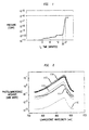
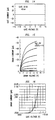
- FIG. 1 shows a schematic curve of pressure vs. time during manufacture in our apparatus of an exemplary GaAs/oxide structure.
- the oxide growth rate is 0.016 nm/s.
- the total exposure is less than about 10 Langmuir.
- the time of completion of the substantially atomically clean (100)-oriented GaAs surface (t c ) is taken to correspond to the origin of the time axis.
- the pressure in the chamber unavoidably rises during deposition above the background pressure. However, in our apparatus completion of the first monolayer of the oxide typically takes only a few seconds (the exact value depending on the deposition rate).
- the O 2 pressure was below the detection limit, and the total background pressure was about 2 x 10 -11 Torr.
- presently preferred embodiments of the invention comprise As-stabilization of the GaAs surface. Exemplarily, this is done by maintaining the As flux after termination of the Ga flux until the sample has cooled to 500°C.
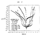
- FIG. 2 shows exemplary photoluminescence data that demonstrates the surprisingly high thermochemical stability of some GaAs/oxide interfaces.
- Curve 110 was obtained from bare GaAs and is provided for comparison purposes.
- the remaining curves were obtained from (100) GaAs/oxide structures according to the invention that were annealed for 120 seconds in forming gas.
- the structures were substantially identical, all having a 26.2 nm SiO 2 cap layer for purposes of the annealing experiment.
- the parameter that distinguishes curves in FIG. 2 is the annealing temperature.
- Curves 111 pertain to 800 and 900°C, 112 to 750 and 1000°C, 113 to 700°C, 114 to 650°C, with the remaining curves (which are almost identical) pertaining to 400, 500, 550 and 600°C, and to an as-deposited structure.
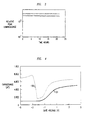
- FIG. 3 shows exemplary photoluminescence data that demonstrates the photochemical stability of an exemplary GaAs/oxide interface.
- Curve 120 pertains to a structure that was annealed at 1000°C for 30 seconds in forming gas, and curve 121 pertains to an analogous as-deposited structure.
- FIG. 4 presents exemplary capacitance vs. gate voltage data for a MOS structure, with curve 130 showing the quasi-static response, and curve 131 showing the high frequency (100 kHz and 1MHz) response.
- the oxide thickness was 46 nm
- the contact size was 2 x 10 -3 cm 2
- the semiconductor was n-type (2 x 10 16 cm -3 )
- the sweep rate was 100 mV/s.
- the data of FIG. 4 demonstrates the existence of inversion as well as of accumulation.
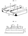
- FIG. 5 schematically depicts an exemplary electronic device, namely, a GaAs-based MOS-FET.
- Numerals 140-147 refer, respectively, to the GaAs body (exemplarily p-type), the source region (exemplarily n-type), the drain region (exemplarily n-type), the drain contact, the source contact, the gate oxide, the gate contact and the field oxide.
- Associated with the interface between 140 and 145 is an interface state density ⁇ 10 11 /cm 2 .eV, and typically a recombination velocity ⁇ 10 4 cm/s.
- FIG. 6 schematically depicts another exemplary electronic device, namely, a GaAs-based HBT.
- Numerals 150-158 refer, respectively, to the collector contact, the GaAs substrate (typically n + ), the GaAs collector layer (typically n - ), the GaAs base layer (typically p + ), the emitter layer (exemplarily n-type graded AlGaAs), the emitter contact layer (exemplarily n + AlGaAs), the base contact, the emitter contact and the oxide passivation layer.
- the oxide passivation layer Associated with the interface between the semiconductor material and oxide layer 158 are the above specified values.
- devices according to the invention are structurally similar or identical to the corresponding (existing or proposed) prior art structures.
- these devices will have substantially improved characteristics.
- the presence of the improved oxide passivation layer will result in significantly reduced recombination in the extrinsic base region, with attendant improvement in device characteristics.
- FIG. 7 shows in flow chart form a MOS-FET manufacturing process according to the instant invention
- FIGs. 8-12 schematically depict various steps of device processing.
- Steps A and B of FIG. 7 respectively require provision of a GaAs substrate and formation of a patterned implant mask.
- the substrate typically is a conventional semi-insulating GaAs wafer, but could be such a wafer with one or more epitaxial layers thereon.
- the discussion below will be in terms of a conventional (100) semi-insulating GaAs substrate.
- Formation of a patterned implant mask exemplarily involves deposition of a thin layer of dielectric material (e.g., SiO 2 , SiN x , SiO x N y , exemplarily 40-200 nm thick) on the major surface of the substrate, deposition of a conventional photoresist layer on the dielectric layer, and patterning of the photoresist layer such that appropriate windows are formed through the photoresist of the dielectric. This is followed by ion implantation (see step C) into the GaAs material that underlies the windows. Steps B and C will typically be repeated one or more times, to attain the dopant distribution shown in FIG. 8. Provision of the dielectric layer is optional but preferred.
- dielectric material e.g., SiO 2 , SiN x , SiO x N y , exemplarily 40-200 nm thick
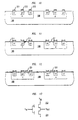
- FIG. 8 shows semi-insulating GaAs substrate 181 and dielectric layer 182. Implanted regions are shown, the implants selected to facilitate formation of a p- MOS-FET 180 and a n-MOS-FET 188. Only the steps leading to formation of the p-MOS-FET will be discussed in detail, since those leading to the n-MOS-FET are either identical or are obvious variations, e.g., substitution of a p-implant for an n-implant.
- n-type region 183 is formed by implantation of Si or S through dielectric layer 182 in photoresist-defined areas of the wafer. After removal of the photoresist mask, a new mask for implantation of additional Si or S into channel contact 184 is provided, and the n + channel contact is formed. This is followed by formation (by Be or Zn implantation) of p + source 185 and p + drain 186. This in turn is optionally followed by formation (by ion implantation) of p source and drain regions 187 and 189, respectively.
- Step D of FIG. 7 involves annealing of the ion implanted substrate under conditions effective for activating the implanted ions, with or without dielectric layer 182 on the substrate.
- the implant activation anneal exemplarily is accomplished in rapid thermal anneal (RTA) apparatus, typically at a temperature in the range 780-860°C for a time in the range 2-5 minutes.
- RTA rapid thermal anneal
- the dielectric layer is removed (e.g., with HF), and the wafer is heated in an evacuable reactor to a temperature in the above range, with the wafer in contact with an As-containing atmosphere.
- the wafer when the wafer reached 300°C, the wafer was maintained at that temperature for 5 minutes under flowing H 2 , followed by heating to 825°C under H 2 and AsH 3 (H 2 : AsH 3 flow 70:1). The wafer was maintained at 825°C for 5 minutes, followed by cooling to room temperature.
- H 2 + arsine elemental arsenic vapor could be used.
- the atmosphere contains enough As or As-containing species (e.g., arsine) to prevent net loss of As from the substrate surface.
- the required partial pressure of As or As-containing species depends inter alia on the annealing temperature, and thus cannot be specificed in generality. However, a minor amount of experimentation will typically suffice to determine appropriate conditions.
- Step E of FIG. 7 typically involves formation of a dielectric layer (exemplarily about 200 nm of SiO 2 ) on the wafer surface, followed by formation of an appropriately patterned photoresist layer that has windows for channel contact, source contact and drain contact. In the window regions, the dielectric material is removed by conventional etch, e.g., with HF.
- numeral 191 refers to the dielectric layer, and 192 to the photoresist.
- Step E of FIG. 7 further comprises deposition of ohmic contacts.
- p-contact metal exemplarily 25 nm AuBe/200 nm Au
- a new photoresist layer is deposited and patterned for n-contact metallization, using, for instance, 5 nm Ni/5 nm Ge/10 nm AuGe/20 nm Mo/200 nm Au.
- FIG. 10 shows the result of the metallization, wherein numeral 201 refers to the n-contact metal of the channel contact, and numerals 202 and 203 refer to the p-contact metal of the source and drain contact, respectively.
- Ohmic contact deposition prior to gate oxide formation is not a requirement, and the deposition could be performed subsequent to gate oxide formation.
- Step F of FIG. 7 involves removal of native oxides (and possibly other contaminants) from the wafer surface.
- the removal has to be carried out such that an essentially atomically clean, essentially atomically ordered, surface results.
- Creation of such a "reconstructed" surface is an important aspect of the process according to the invention. It can be accomplished in any appropriate manner, and will typically be carried out under high vacuum (e.g., pressure ⁇ 10 -8 Torr).
- high vacuum e.g., pressure ⁇ 10 -8 Torr.
- thermal desorption e.g., 5 minutes at 580°C, As overpressure at 10 -6 Torr to protect the wafer surface
- low damage dry etching techniques such as ECR with H 2 plasma or atomic hydrogen.
- the gate oxide layer is formed (step G of FIG. 7) in situ on the reconstructed surface, i.e., without removal of the wafer from the high vacuum. Not only is the oxide layer grown in situ, but the time between completion of surface reconstruction and commencement of oxide deposition is desirably kept to a minimum, in order to avoid significant (e.g., in excess of 100 Langmuirs) contamination of the surface.
- the wafer is maintained at a temperature of at most 580°C under arsenic overpressure (e.g., 10 -6 Torr As) during gate oxide deposition.
- arsenic overpressure e.g. 10 -6 Torr As
- the oxide typically is deposited substantially uniformly over the whole wafer surface, but deposition could, at least in principle, be limited to particular portions of the surface, these portions including the gate region between source and drain of at least one MOS-FET. Further details of gate oxide formation are discussed below.
- the oxide is patterned to expose the previously formed channel, source and drain contacts of the MOS-FETs, as indicated by step H of FIG. 7.
- the patterning can be done using conventional photolithography and etching, e.g., in HCl solution.
- FIG. 11 schematically shows two devices after gate oxide patterning with numeral 211 referring to the patterned gate oxide.
- Patterning of the gate oxide layer is followed by gate metallization, also per step H of FIG. 7.
- This can be conventional, involving for instance e-beam deposition of 25 mm Ti/50 nm Pt/300 nm Au, and lift-off.
- this step can also include formation of interconnections, including providing connections (not shown in FIG. 12) to channel, source, drain and gate contacts of the various MOS-FETs.
- numerals 221 and 222 refer to the gate contact of the p-MOS-FET and n-MOS-FET, respectively.
- Step I of FIG. 7 refers to a variety of, typically conventional, steps that will typically be required to complete an IC according to the invention, e.g., testing, dicing of the wafer into chips, wire bonding, encapsulation, etc.
- MOS-FET desirably will be electrically connected in conventional manner to other electronic devices, including other MOS-FETs, to form an integrated circuit.
- the complementary MOS-FETs of FIG. 12 can be connected as shown in FIG. 13 to provide an inverter.
- numeral 231 refers to a n-channel enhancement mode GaAs MOS-FET substantially as shown in FIG. 12
- 232 refers to a p-channel enhancement mode GaAs MOS-FET, also substantially as shown in FIG. 12.
- the circuit per se is conventional, but the implementation in GaAs MOS-FET technology is novel, to the best of our knowledge.
- the combination of FIG. 13 is representative of circuits according to the invention.
- the above described process not only is suitable for producing GaAs-based planar n-channel and p-channel MOS-FETs on the same substrate, but can also be used to combine such MOS-FETs with GaAs (metal-semiconductor) MES-FETs.
- the gate oxide exemplarily is removed from the respective gate region, and an appropriate metal (e.g., Ti/Pt/Au) is deposited in the gate region to provide a Schottky barrier contact.
- GaAs-based MES-FETs are known and do not require detailed description.
- GaAs MES-FETs with GaAs MOS-FETs (including complementary enhancement type GaAs-MOSFETs) does, to the best of our knowledge, not exist in the prior art. Availability of this ability is expected to provide circuit designers with greater design freedom, and to lead to manufacture of a wide range of GaAs-based digital (but not excluding analog) ICs.
- GaAs MOS-FETs Some differences between prior art GaAs MOS-FETs and GaAs MOS-FETs according to the invention may bear further recitation.
- the source and drain regions are connected by a channel of the same conductivity type as the regions. See, for instance, the above cited paper by Colquhoun et al. Such devices do not exhibit inversion in the channel.
- Some prior art devices require selective etching of the surface of the GaAs wafer, typically to form a notch in the surface to thereby reduce the channel width. See, for instance, the above cited paper by T. Mimura et al., FIGs. 7 and 8, and the Colquhoun et al. paper. No such etching is required for GaAs MOS-FETs according to the invention.
- ohmic contacts can be formed after gate oxide deposition.
- oxide layers as described above can also be used for passivation purposes, exemplarily for opto-electronic devices.
- Non-optional features of the inventive process which are currently deemed necessary for the production of GaAs-based MOS-FETs of acceptable characteristics.
- reconstruction of the relevant areas of the implanted wafer such that the surface areas are essentially atomically clean and ordered, and in situ growth of the gate oxide on the reconstructed surface regions.
- the method is carried out such that the device is, after gate oxide formation, not subjected to a temperature above about 300°C in air, or ⁇ 700°C in UHV.
- a highly preferred feature is implant activation anneal in an As-containing atmosphere, with the partial pressure of As or As-containing species selected to prevent net loss of As from the surface.
- MOS-FETs produced according to the invention have been tested in conventional fashion, and have been found to have excellent characteristics.
- the '768 patent teaches use of different evaporation source materials that "contain” Ga 2 O 3 and another oxide having a melting temperature that is more than 700° C above the sublimation temperature of Ga 2 O 3 .
- One such material is MgGa 2 O 4 , which is said to "contain” MgO and Ga 2 O 3 .
- MgGa 2 O 4 instead of GGG is said to result in " ⁇ drastically reduced incorporation of the undesired specie in the oxide film and in significantly lower bulk trap density in the oxide film.” See col. 3, lines 18-21 of the '768 patent. However, the '768 patent does not provide any experimental data.
- the oxide thin film desirably contains a substantial amount of Gd (or other appropriate metal element).
- Gd or other appropriate metal element
- a film that is formed by evaporation from pure Ga 2 O 3 powder (and thus is essentially pure Ga oxide) is generally not of device quality
- a film that is formed by evaporation from pure Gd 2 O 3 (and thus is essentially pure Gd oxide) is generally of device quality, with low interface state density.
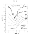
- FIG. 17 shows data on the I-V (current-voltage) characteristics of very thin oxide layers on GaAs, with a conventional metal contact defining the area of the MOS capacitor.
- a 40 nm thick Ga 2 O 3 film has essentially zero breakdown voltage for negative bias, with relatively high leakage for positive bias, and thus is unsuitable for most device applications, whereas a 18.5 nm thick Gd 2 O 3 film conducts a mere 10 -8 A/cm 2 at + or -3V.
- Films of intermediate composition show intermediate breakdown voltages.
- a thin oxide film that is formed by in situ coevaporation from two separate sources generally will be of device quality, provided the evaporation rates are selected such that the content of Gd (or other appropriate metal element) is at least about 10 atomic % of the total metal content, preferably at least 20 atomic %.
- GaAs substrates were prepared as described above (resulting in an essentially atomically clean and atomically ordered surface), with the evaporations carried out in situ, without exposure of the samples to the atmosphere.
- Ga can exist in the 1+, 2+ and 3+ oxidation states, and that there are electro-positive elements (to be termed "stabilizers") that can stabilize Ga in the 3+ state.
- the stabilizers for Ga is Gd, having Pauling electronegativity 1.1.
- the stabilizers for Ga are Sc, Y, the other rare earths, the alkaline earths and the alkalis.
- the oxide film is formed by deposition from 2 (or more) separate deposition sources (e.g., e-beam evaporation sources), with the deposition parameters selected such that the resulting film has overall composition Ga x A y O z , where A is one or more electropositive stabilizer element for stabilizing Ga in the 3+ oxidation state, and x > 0.
- y/(x+y) is greater than or equal to 0.1, preferably ⁇ 0.2, and z is selected to satisfy the requirement that both Ga and A are substantially fully oxidized.
- the oxide film is formed by deposition of A-oxide, without deposition of Ga-oxide.
- the film thus has overall composition AO z , with z selected such that A is substantially fully oxidized.
- A is selected from the group consisting of Sc, Y, the rare earth metals (atomic number 57-71), the alkaline earths (e.g., Be, Mg, Ca, Sr, Ba), and the alkalis (e.g., Li, Na, K, Rb, Cs).
- the alkali elements generally are not preferred, due to their relative instability to moisture and incompatibility with semiconductor device processing conditions.
- the currently preferred stabilizer elements are Sc, Y, the rare earths (atomic number 57-71) and the alkaline earths, with Sc, Y, La, Nd, Gd, Dy, Ho, Er and Lu being currently most preferred.
- Ga (and A) are substantially fully oxidized does not mean that 100% of all Ga ions have to be in the 3+ ionization state. Typically acceptable results are obtained if 80% or more of all Ga is in the 3+ state, with 80% or more of A also being fully oxidized.
- a mixed oxide of composition Ga x A y y O z is not necessarily a homogeneous material of that composition.
- the material contains microscopic regions of Ga-oxide as well as microscopic regions of A-oxide.
- FIG. 18 shows C-V (capacitance-voltage) data for a 19 nm thick film of Gd 2 O 3 on n-type (4.10 17 cm -3 ) GaAs of (100) orientation.
- the area of the MOS capacitor was 4.4 x 10 -5 cm 2 .
- FIG. 18 clearly shows accumulation and inversion at low frequency. The data establishes the suitability of the oxide film for device applications, including for MOS-FETs.
- FIG. 19 shows similar data for a 32 nm thick Ga- and Gd-containing mixed oxide film, with about 22 atomic % of the total metal content being Gd.
- the data also shows accumulation and inversion, substantially as the data of FIG. 18.
- the article comprises a planar enhancement mode MOS-FET with inversion channel.
- a p-MOS-FET was fabricated as follows.
- a conventional semi-insulating (100) oriented GaAs wafer (sheet resistivity about 10 8 ⁇ cm) was provided.
- a 50 nm layer of SiO 2 was deposited, by conventional PECVD, a 50 nm layer of SiO 2 .
- a 2.2 ⁇ m layer of conventional photoresist (AZ 1818) was formed on the SiO 2 layer and patterned to form an ion implantation mask, with a window through the mask that defined the n channel for the p-MOS-FET.
- Si ions were then implanted through the window (150 keV, 5 x 10 13 cm -2 ).
- Implant conditions were, respectively, as follows: 75 KeV, 6 x 10 13 cm -2 , Si; 30 KeV, 7 x 10 13 cm -2 , Be; and 25 KeV, 3 x 10 12 cm -2 , Be.
- the resist and SiO 2 were removed with acetone and HF (1:1 HF: H 2 O), respectively.
- Implant activation was carried out in the reactor of a MOCVD system. The temperature of the wafer was raised, with H 2 admitted into the reactor when the wafer temperature had reached 300°C. The wafer was maintained under these conditions for 5 minutes, followed by admission of arsine and raising of the temperature to 825°C, and maintenance of the wafer under these conditions for 5 minutes.
- the arsine: H 2 flow ratio and system pressure were 1:70 and 45 Torr, respectively.
- the wafer was allowed to cool to 450°C under arsine/H 2 , and then to room temperature under H 2 , and transferred to a MBE system for surface reconstruction and gate oxide deposition.
- the wafer was mounted on a Mo block with indium and heated to 580°C for 5 minutes to desorb surface contaminants such as native oxides.
- the background pressure in the reactor of the MBE system was 10 -10 Torr, and an arsenic pressure of 10 -6 Torr was maintained in the reactor to protect the wafer surface.
- RHEED was used to monitor the sample surface. The above described treatment resulted in an essentially atomically clean, atomically ordered wafer surface.
- the wafer Upon completion of surface reconstruction, the wafer was transferred under UHV (10 -10 Torr) to a second chamber of the MBE system.
- a 40 nm layer of Ga-Gd-oxide is deposited over the wafer surface at a rate of about 0.02 nm/sec.
- the wafer is at 550°C
- the background pressure in the chamber is less than 10 -9 Torr
- the Ga-Gd-oxide is formed by simultaneous e-beam evaporation from Gd 2 O 3 powder and Ga 2 O 3 powder, with deposition conditions adjusted such that the resulting Ga-Gd-oxide layer has overall composition Ga x Gd y O z , with x being about 0.8 and y being about 0.2.
- the oxygen content is selected such that both Ga and Gd are fully oxidized, exemplarily z is about 3.
- a conventional photoresist layer (AZ 1818) is applied and patterned in conventional manner such that the gate source and drain contact regions are exposed.
- the gate oxide is then removed from the exposed regions with 1:1 HCl:H 2 O, and contact metal (25 nm AuBe/200 nm Au) is deposited by means of an e-beam deposition system.
- a conventional acetone lift-off technique is used to remove the undesired metallization.
- a 1.2 ⁇ m resist layer (AZ 1811) is applied and patterned, and used to define gate and final metal contacts at the same time.
- a Pt/Ti/Pt/Au layer (5 nm/25 nm/50 nm/300 nm, respectively) is deposited by means of an e-beam deposition system. Unwanted metallization is removed with a conventional acetone lift-off technique, leaving channel, source, drain and gate contacts.
- the thus produced device (40 x 50 ⁇ m 2 gate geometry) is tested, and is found to have characteristics substantially as shown in FIGs. 14-16.
- the gate oxide has breakdown voltage of about 3.6 x 10 6 Volt/cm.
- the transconductance is about 0.3 mS/mm.
- FIG. 15 shows the drain I-V characteristics and FIG. 16 shows drain current vs. gate voltage.
- a pair of complementary MOS-FETs on a common substrate are produced substantially as described above, except that the ion implantation is modified to produce implanted regions substantially as shown in FIG. 8.
- the pair of MOS-FETs is connected as shown in FIG. 13 to form an inverter circuit. The circuit is tested and performs as expected.
- a multiplicity of n-MOS-FETs, p-MOS-FETs and n- and p-MES-FETs are formed on a common substrate, substantially as described in Example 2, except that the gate oxide is removed from some of the n-type devices and some of the p-type devices, and 5 nm Pt/25 nm Ti/30 nm Pt/300 nm Au is deposited in the gate regions of these devices. After provision of conductive interconnects between the devices, the resulting circuit is tested and performs as expected.
- a MOS-FET is fabricated substantially as in Example 1, except that the oxide deposition conditions are selected such that the gate oxide film is Gd 2 O 3 .
- the MOS-FET performs substantially as the device of Example 1.
Landscapes
- Chemical & Material Sciences (AREA)
- Engineering & Computer Science (AREA)
- Metallurgy (AREA)
- Chemical Kinetics & Catalysis (AREA)
- Organic Chemistry (AREA)
- Mechanical Engineering (AREA)
- Materials Engineering (AREA)
- Insulated Gate Type Field-Effect Transistor (AREA)
- Power Engineering (AREA)
- Condensed Matter Physics & Semiconductors (AREA)
- General Physics & Mathematics (AREA)
- Microelectronics & Electronic Packaging (AREA)
- Physics & Mathematics (AREA)
- Computer Hardware Design (AREA)
- Manufacturing & Machinery (AREA)
- Electrodes Of Semiconductors (AREA)
- Junction Field-Effect Transistors (AREA)
- Bipolar Transistors (AREA)
- Metal-Oxide And Bipolar Metal-Oxide Semiconductor Integrated Circuits (AREA)
Applications Claiming Priority (2)
| Application Number | Priority Date | Filing Date | Title |
|---|---|---|---|
| US122558 | 1980-02-19 | ||
| US09/122,558 US6271069B1 (en) | 1994-03-23 | 1998-07-24 | Method of making an article comprising an oxide layer on a GaAs-based semiconductor body |
Publications (2)
| Publication Number | Publication Date |
|---|---|
| EP0975013A2 true EP0975013A2 (de) | 2000-01-26 |
| EP0975013A3 EP0975013A3 (de) | 2000-05-10 |
Family
ID=22403411
Family Applications (1)
| Application Number | Title | Priority Date | Filing Date |
|---|---|---|---|
| EP99305512A Withdrawn EP0975013A3 (de) | 1998-07-24 | 1999-07-12 | Verfahren zur Herstellung einer Oxydschicht auf einen GaAs-basierten Halbleiterkörper |
Country Status (4)
| Country | Link |
|---|---|
| US (1) | US6271069B1 (de) |
| EP (1) | EP0975013A3 (de) |
| JP (1) | JP2000101081A (de) |
| KR (1) | KR20000011954A (de) |
Cited By (1)
| Publication number | Priority date | Publication date | Assignee | Title |
|---|---|---|---|---|
| CN111463129A (zh) * | 2020-06-18 | 2020-07-28 | 浙江集迈科微电子有限公司 | 基于原位钝化及氧化工艺的GaN器件及其制备方法 |
Families Citing this family (8)
| Publication number | Priority date | Publication date | Assignee | Title |
|---|---|---|---|---|
| US6326732B1 (en) * | 1999-02-16 | 2001-12-04 | International Business Machines Corporation | Apparatus and method for non-contact stress evaluation of wafer gate dielectric reliability |
| US6756320B2 (en) * | 2002-01-18 | 2004-06-29 | Freescale Semiconductor, Inc. | Method of forming article comprising an oxide layer on a GaAs-based semiconductor structure |
| US7442654B2 (en) * | 2002-01-18 | 2008-10-28 | Freescale Semiconductor, Inc. | Method of forming an oxide layer on a compound semiconductor structure |
| JP2004193332A (ja) * | 2002-12-11 | 2004-07-08 | Oki Electric Ind Co Ltd | 成膜方法 |
| US6963090B2 (en) * | 2003-01-09 | 2005-11-08 | Freescale Semiconductor, Inc. | Enhancement mode metal-oxide-semiconductor field effect transistor |
| US20100244105A1 (en) * | 2009-03-31 | 2010-09-30 | Kiuchul Hwang | Transistors having temperature stable schottky contact metals |
| FI20106181A0 (fi) * | 2010-11-11 | 2010-11-11 | Pekka Laukkanen | Menetelmä substraatin muodostamiseksi ja substraatti |
| FI128613B (en) * | 2019-06-19 | 2020-08-31 | Comptek Solutions Oy | Optoelectronic device |
Family Cites Families (3)
| Publication number | Priority date | Publication date | Assignee | Title |
|---|---|---|---|---|
| US3663870A (en) | 1968-11-13 | 1972-05-16 | Tokyo Shibaura Electric Co | Semiconductor device passivated with rare earth oxide layer |
| JPH0682651B2 (ja) | 1985-05-30 | 1994-10-19 | 株式会社日立製作所 | 半導体装置用エピタキシヤル絶縁膜とその製造方法 |
| US5903037A (en) | 1997-02-24 | 1999-05-11 | Lucent Technologies Inc. | GaAs-based MOSFET, and method of making same |
-
1998
- 1998-07-24 US US09/122,558 patent/US6271069B1/en not_active Expired - Lifetime
-
1999
- 1999-07-12 EP EP99305512A patent/EP0975013A3/de not_active Withdrawn
- 1999-07-23 JP JP11208326A patent/JP2000101081A/ja active Pending
- 1999-07-24 KR KR1019990030180A patent/KR20000011954A/ko not_active Withdrawn
Cited By (1)
| Publication number | Priority date | Publication date | Assignee | Title |
|---|---|---|---|---|
| CN111463129A (zh) * | 2020-06-18 | 2020-07-28 | 浙江集迈科微电子有限公司 | 基于原位钝化及氧化工艺的GaN器件及其制备方法 |
Also Published As
| Publication number | Publication date |
|---|---|
| US6271069B1 (en) | 2001-08-07 |
| KR20000011954A (ko) | 2000-02-25 |
| EP0975013A3 (de) | 2000-05-10 |
| JP2000101081A (ja) | 2000-04-07 |
Similar Documents
| Publication | Publication Date | Title |
|---|---|---|
| US5962883A (en) | Article comprising an oxide layer on a GaAs-based semiconductor body | |
| US6469357B1 (en) | Article comprising an oxide layer on a GaAs or GaN-based semiconductor body | |
| US5616947A (en) | Semiconductor device having an MIS structure | |
| US4477311A (en) | Process and apparatus for fabricating a semiconductor device | |
| EP0561567A2 (de) | Legierungen die Gallium und Aluminium enthalten, für Halbleiterkontakte | |
| US9780190B2 (en) | InP-based transistor fabrication | |
| US7187045B2 (en) | Junction field effect metal oxide compound semiconductor integrated transistor devices | |
| US20110233689A1 (en) | Semiconductor device, process for producing semiconductor device, semiconductor substrate, and process for producing semiconductor substrate | |
| Ohmi | ULSI reliability through ultraclean processing | |
| US6989556B2 (en) | Metal oxide compound semiconductor integrated transistor devices with a gate insulator structure | |
| KR900005560B1 (ko) | 반도체장치 및 그 제조방법 | |
| US6271069B1 (en) | Method of making an article comprising an oxide layer on a GaAs-based semiconductor body | |
| EP0863552B1 (de) | GaAs-basierender MOSFET und Verfahren zur Herstellung | |
| KR100516252B1 (ko) | 반도체소자를가진물품및그제조방법 | |
| EP0208851B1 (de) | Herstellung eines Halbleiterbauelementes mittels Molekularstrahlepitaxie | |
| EP0987746B1 (de) | Methode zur Herstellung einer integrierten Schaltung mit einer Oxidschicht auf einem GaAs Halbleitersubstrat | |
| US5399900A (en) | Isolation region in a group III-V semiconductor device and method of making the same | |
| KR900001233B1 (ko) | 고캐리어 농도를 갖는 화합물 반도체층 및 그의 제조방법 | |
| JP3126890B2 (ja) | Mis構造を有する半導体装置及びその製造方法 | |
| Ohmi | Technology for High-Power Devices | |
| Murakami et al. | Effects of interfacial microstructure on ohmic contacts to GaAs | |
| JPH1174515A (ja) | 化合物半導体装置の製造方法及び化合物半導体装置 | |
| JPH11274168A (ja) | ヘテロ接合バイポーラトランジスタの製造方法 | |
| Jiang et al. | P-type doping of GaAs by carbon implantation | |
| Luo et al. | GROWTH OF MAGNESIUM OXIDE AND SCANDIUM OXIDE ON GaN FOR USE AS GATE AND FIELD PASSIVATION DIELECTRICS |
Legal Events
| Date | Code | Title | Description |
|---|---|---|---|
| PUAI | Public reference made under article 153(3) epc to a published international application that has entered the european phase |
Free format text: ORIGINAL CODE: 0009012 |
|
| AK | Designated contracting states |
Kind code of ref document: A2 Designated state(s): DE FR GB |
|
| AX | Request for extension of the european patent |
Free format text: AL;LT;LV;MK;RO;SI |
|
| PUAL | Search report despatched |
Free format text: ORIGINAL CODE: 0009013 |
|
| AK | Designated contracting states |
Kind code of ref document: A3 Designated state(s): AT BE CH CY DE DK ES FI FR GB GR IE IT LI LU MC NL PT SE |
|
| AX | Request for extension of the european patent |
Free format text: AL;LT;LV;MK;RO;SI |
|
| 17P | Request for examination filed |
Effective date: 20001026 |
|
| AKX | Designation fees paid |
Free format text: DE FR GB |
|
| STAA | Information on the status of an ep patent application or granted ep patent |
Free format text: STATUS: THE APPLICATION IS DEEMED TO BE WITHDRAWN |
|
| 18D | Application deemed to be withdrawn |
Effective date: 20050201 |