EP0974247B1 - Schaltungsanordnung zum betrieb mindestens einer elektrodenlosen entladungslampe - Google Patents
Schaltungsanordnung zum betrieb mindestens einer elektrodenlosen entladungslampe Download PDFInfo
- Publication number
- EP0974247B1 EP0974247B1 EP99907281A EP99907281A EP0974247B1 EP 0974247 B1 EP0974247 B1 EP 0974247B1 EP 99907281 A EP99907281 A EP 99907281A EP 99907281 A EP99907281 A EP 99907281A EP 0974247 B1 EP0974247 B1 EP 0974247B1
- Authority
- EP
- European Patent Office
- Prior art keywords
- circuit
- discharge lamp
- circuit arrangement
- voltage
- electrodeless discharge
- Prior art date
- Legal status (The legal status is an assumption and is not a legal conclusion. Google has not performed a legal analysis and makes no representation as to the accuracy of the status listed.)
- Expired - Lifetime
Links
- 230000006698 induction Effects 0.000 claims description 32
- 238000012544 monitoring process Methods 0.000 claims description 10
- 238000011156 evaluation Methods 0.000 claims description 8
- 230000005684 electric field Effects 0.000 claims description 2
- 239000003990 capacitor Substances 0.000 description 78
- 238000010586 diagram Methods 0.000 description 10
- 238000011144 upstream manufacturing Methods 0.000 description 4
- 238000004804 winding Methods 0.000 description 4
- 230000010355 oscillation Effects 0.000 description 3
- 101001114407 Haloarcula marismortui (strain ATCC 43049 / DSM 3752 / JCM 8966 / VKM B-1809) 30S ribosomal protein S6e Proteins 0.000 description 2
- 101000718286 Halobacterium salinarum (strain ATCC 700922 / JCM 11081 / NRC-1) 30S ribosomal protein S13 Proteins 0.000 description 2
- 230000002950 deficient Effects 0.000 description 2
- 230000000052 comparative effect Effects 0.000 description 1
- 230000006378 damage Effects 0.000 description 1
- 230000001066 destructive effect Effects 0.000 description 1
- 238000001514 detection method Methods 0.000 description 1
- 238000000034 method Methods 0.000 description 1
- 230000001681 protective effect Effects 0.000 description 1
- 238000010079 rubber tapping Methods 0.000 description 1
- 229910000859 α-Fe Inorganic materials 0.000 description 1
Images


Classifications
-
- H—ELECTRICITY
- H05—ELECTRIC TECHNIQUES NOT OTHERWISE PROVIDED FOR
- H05B—ELECTRIC HEATING; ELECTRIC LIGHT SOURCES NOT OTHERWISE PROVIDED FOR; CIRCUIT ARRANGEMENTS FOR ELECTRIC LIGHT SOURCES, IN GENERAL
- H05B41/00—Circuit arrangements or apparatus for igniting or operating discharge lamps
- H05B41/14—Circuit arrangements
- H05B41/26—Circuit arrangements in which the lamp is fed by power derived from DC by means of a converter, e.g. by high-voltage DC
- H05B41/28—Circuit arrangements in which the lamp is fed by power derived from DC by means of a converter, e.g. by high-voltage DC using static converters
- H05B41/2806—Circuit arrangements in which the lamp is fed by power derived from DC by means of a converter, e.g. by high-voltage DC using static converters with semiconductor devices and specially adapted for lamps without electrodes in the vessel, e.g. surface discharge lamps, electrodeless discharge lamps
- H05B41/2813—Arrangements for protecting lamps or circuits against abnormal operating conditions
-
- Y—GENERAL TAGGING OF NEW TECHNOLOGICAL DEVELOPMENTS; GENERAL TAGGING OF CROSS-SECTIONAL TECHNOLOGIES SPANNING OVER SEVERAL SECTIONS OF THE IPC; TECHNICAL SUBJECTS COVERED BY FORMER USPC CROSS-REFERENCE ART COLLECTIONS [XRACs] AND DIGESTS
- Y02—TECHNOLOGIES OR APPLICATIONS FOR MITIGATION OR ADAPTATION AGAINST CLIMATE CHANGE
- Y02B—CLIMATE CHANGE MITIGATION TECHNOLOGIES RELATED TO BUILDINGS, e.g. HOUSING, HOUSE APPLIANCES OR RELATED END-USER APPLICATIONS
- Y02B20/00—Energy efficient lighting technologies, e.g. halogen lamps or gas discharge lamps
-
- Y—GENERAL TAGGING OF NEW TECHNOLOGICAL DEVELOPMENTS; GENERAL TAGGING OF CROSS-SECTIONAL TECHNOLOGIES SPANNING OVER SEVERAL SECTIONS OF THE IPC; TECHNICAL SUBJECTS COVERED BY FORMER USPC CROSS-REFERENCE ART COLLECTIONS [XRACs] AND DIGESTS
- Y10—TECHNICAL SUBJECTS COVERED BY FORMER USPC
- Y10S—TECHNICAL SUBJECTS COVERED BY FORMER USPC CROSS-REFERENCE ART COLLECTIONS [XRACs] AND DIGESTS
- Y10S315/00—Electric lamp and discharge devices: systems
- Y10S315/07—Starting and control circuits for gas discharge lamp using transistors
Definitions
- the invention relates to a circuit arrangement for operating at least one electrodeless Discharge lamp according to the preamble of patent claim 1.
- the term electrodeless discharge lamp here denotes an inductively excited one Gas discharge lamp.
- This gas discharge lamp has a translucent discharge vessel with an included ionizable, stimulable for gas discharge Filling.
- the gas discharge is excited by means of one or more Induction coils with closed ferrite core, the outside of the discharge vessel are attached.
- the induction coils with a high frequency AC voltage are applied, are arranged such that they create an electric field in the discharge vessel Feed in the ionizable filling inside the discharge vessel stimulates gas discharge.
- This gas discharge has - in difference to the gas discharge that occurs in the widely used fluorescent lamps in the discharge vessel protruding electrodes takes place - a closed ring Discharge.
- a more detailed description of an electrodeless discharge lamp is, for example, in international laid-open publication WO 97/10610 disclosed.
- the invention particularly relates to a circuit arrangement for operation such an electrodeless discharge lamp.
- a circuit arrangement corresponding to the preamble of claim 1 is described, for example, in US Pat. No. 5,063,332.
- This circuit arrangement has a half-bridge inverter with a resonance circuit to which the induction coil of an electrodeless discharge lamp is connected is.
- a disadvantage of this circuit arrangement is that it is also works with missing lamp.
- the laid-open specification WO 96/30983 discloses a circuit arrangement for a Fluorescent lamp with an inverter, a control circuit for the inverter and a protective circuit for detecting the lamp current.
- the protection circuit is coupled to the control circuit so that the inverter is switched off if no lamp is connected.
- the published patent application EP 0 198 632 A2 discloses a circuit arrangement for Fluorescent lamps with a transistor oscillator and defective detection means Lamp electrodes and for switching off the transistor oscillator in the case of one defective lamp electrode.
- the circuit arrangement according to the invention for operating at least one electrodeless Discharge lamp has at least one voltage input for voltage supply the circuitry and electrical connections for at least an electrodeless discharge lamp and is according to the invention with control means equipped, the presence or absence of at least one electrodeless Determine discharge lamp and the provision of the ignition and / or operating voltage only then for the at least one electrodeless discharge lamp enable when the at least one electrodeless discharge lamp connected to the electrical Connections is connected.
- the control means of the invention Circuit arrangements have a current path and a current or voltage detector on, the current path having a first electrical resistance value, if the at least one discharge lamp is connected to the circuit arrangement and has a different electrical resistance when there is no discharge lamp is connected to the circuit arrangement, and the current or voltage detector the current flow or the voltage drop in the current path supervised.
- To the presence or absence of at least one electrodeless To be able to determine discharge lamp with simple means is at least one Induction coil of the at least one electrodeless discharge lamp in the Current path arranged.
- the current path is advantageously designed such that it is interrupted in the absence of the at least one electrodeless discharge lamp is.
- the electrical connections for the at least one are electrodeless Discharge lamp advantageously arranged in the current path. With the current path it is advantageously a direct current path.
- the circuit arrangement according to the invention advantageously has at least a voltage converter and a control circuit for the at least one voltage converter as well as one downstream of the at least one voltage converter Load circuit, the control means cooperating with the control circuit in such a way that the control circuit only then drive pulses for the least a voltage converter is generated if the at least one electrodeless Discharge lamp is connected to the electrical connections.
- This can the voltage converter only starts operating when the minimum an electrodeless discharge lamp to the electrical connections provided connected.
- the voltage converter is advantageously an inverter formed with a downstream resonant circuit so that the ignition the gas discharge required in the at least one electrodeless discharge lamp Ignition voltage in a simple manner by means of the method of excessive resonance can be generated.
- the control circuit of the voltage divider is advantageous designed as an integrated circuit.
- a circuit arrangement for operation has at least been particularly advantageous an electrodeless discharge lamp with at least one voltage input for Power supply for the circuit arrangement and electrical connections for proven at least one electrodeless discharge lamp, the at least one Voltage converter and a control circuit designed as an integrated circuit for the at least one voltage converter and one for the at least one Voltage converter downstream load circuit, and that as a control means, which indicates the presence or absence of at least one electrodeless discharge lamp on the electrical connections and the provision of the Ignition or operating voltage for the at least one electrodeless discharge lamp only allow if the at least one Electrodeless discharge lamp connected to the electrical connections is, one to a voltage supply connection of the integrated Circuit connected current path, which in the absence of at least one electrodeless discharge lamp at the electrical connections is interrupted. If there is no lamp, this will give the Integrated circuit controlling at least one voltage converter no supply voltage, so that the voltage converter defies its operation switched on mains voltage at the voltage input of the circuit arrangement - cannot record.
- control means comprise advantageously a tap in the load circuit of the at least one Voltage converter and a monitoring element, the electrical Potential at this tap has a first value if the minimum a discharge lamp is connected to the circuit arrangement, and has a second, different value if no discharge lamp is connected to the Circuit arrangement is connected, and wherein the monitoring element the electrical potential at the tap is monitored and the electrical one Potential corresponding evaluation signal for the control circuit of the generated at least one voltage converter.
- the monitoring link is advantageously designed as a logic circuit, which in the control circuit integrated or upstream of the control circuit.
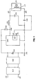
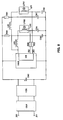
- the circuit arrangement according to the first embodiment of the invention has a mains voltage input with the mains voltage connections j10, j11, which supply voltage to the circuit arrangement serve.
- a filter and a filter are connected to the mains voltage input downstream mains voltage rectifier GL1 connected.
- the filter reduces the amount fed into the power grid by the circuit arrangement high-frequency voltage components.
- To the DC voltage output a step-up converter HS1 is connected to the mains voltage rectifier GL1, which ensures a sinusoidal current draw from the power grid.
- An intermediate circuit capacitor is connected in parallel to the output of the step-up converter HS1 C10 switched on which the supply voltage for the downstream half-bridge inverter HW1 is provided.
- the control of the switching transistors of the half-bridge inverter HW1 and also the step-up converter HS1 takes place with the help of the integrated Circuit IC1, its supply voltage via the voltage supply connection J14 and another grounding j15 receives.
- On the half-bridge inverter HW1 is a resonance circuit trained load circuit connected to the resonance inductance L10, the Capacitors C11, C12 and the electrical connections j12, j13.
- the electrical connections j12, j13 are parallel to the capacitors C11, C12 switched and are used to connect the electrodeless discharge lamp LP1, that is, for connecting at least one induction coil L11 the electrodeless discharge lamp LP1.
- One connection of the capacitors C10, C11, C12 is at the branch point on ground V11 connected.
- the capacitor C12 decouples the connection j13 DC from the ground terminal V11.
- the first exemplary embodiment shown in FIG. 1 also has an ohmic resistor R10, on the one hand with the positive pole of the intermediate circuit capacitor C10 and on the other hand with the tap V10 is connected in the load circuit.
- the supply current for the integrated Circuit IC1 flows from the positive pole of the intermediate circuit capacitor C10, via the resistor R10, the resonance inductance L10, the electrical connection j12, the at least one induction coil L11 of the electrodeless Discharge lamp LP1 and the electrical connection j13 to positive voltage connection j14 of the integrated circuit IC1.
- the lamp LP1 is missing, that is, if the induction coil is not connected L11 the DC path between the connections j12, j13 is interrupted. Then the integrated circuit receives IC1, despite at the voltage input j10, j11 mains voltage present, no supply voltage. As a result, neither the half-bridge inverter HW1 nor the Boost converter HS1 commence operation. The start of the half-bridge inverter HW1 and the step-up converter HS1 only takes place after previously the DC path by connecting the at least one Induction coil L11 of the lamp LP1 closed at the connections j12, j13 has been.
- the electrodeless discharge lamp LP1 has several Induction coils L11, for example two, so these induction coils also connected to terminals j12, j13, so that they are parallel are connected to the induction coil L11.
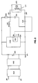
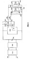
- FIG 2 is the second embodiment of the circuit arrangement according to the invention shown in a schematic representation.
- the circuit arrangement according to the second embodiment has a mains voltage input with the mains voltage connections j20, j21, one filter and one Mains voltage rectifier GL2, a downstream step-up converter HS2, one connected to the output of the step-up converter HS2 DC link capacitor C20, the supply voltage for one Half-bridge inverter HW2 delivers.
- the half-bridge inverter HW2 is connected downstream of a load circuit designed as a resonance circuit Resonance inductor L20, the capacitors C21, C22 and two electrical Has connections j22, j23 for an electrodeless discharge lamp LP2.
- the half-bridge inverter HW2 is controlled with the help an integrated circuit IC2, which also the drive pulses for generates the step-up converter HS2.
- the integrated circuit IC2 is about the terminal j25 on the ground and the other terminal j24 its Supply voltage supplied.
- the circuit arrangement has an ohmic resistor R20, on the one hand to the positive pole of the intermediate circuit capacitor C20 and on the other hand to a tap between the resonance inductance L20 and the electrical connection j22 in Load circuit is connected.
- the supply current for the integrated Circuit IC2 flows from the positive pole of the intermediate circuit capacitor C20, via the resistor R20, the electrical connection j22, the at least one induction coil L21 of the electrodeless discharge lamp LP2 and the electrical connection j23 to the positive voltage supply connection j24 of the integrated circuit IC2.
- the capacitor C22 DC-decouples terminal j23 from the ground terminal V21.
- the lamp LP2 is missing, that is, if the induction coil is not connected L21 the direct current path between the connections j22, j23 is interrupted. Then the integrated circuit receives IC2, despite at the voltage input j20, j21 mains voltage present, no supply voltage. As a result, neither the half-bridge inverter HW2 nor the Boost converter HS2 commence operation.
- the circuit arrangement this second embodiment differs from that of the first Embodiment only in that the resonance inductance L20 of second embodiment, in contrast to that of the first embodiment, is not connected to the DC path.
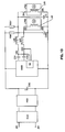
- the third exemplary embodiment of the invention shown in FIG. 3 has a mains voltage input with the mains voltage connections j30, j31, a filter and a mains voltage rectifier GL3, a downstream one Step-up converter HS3, one to the output of the step-up converter HS3 connected DC link capacitor C30, the supply voltage for an HW3 inverter.
- the inverter HW3 is a Load circuit designed as a resonance circuit which connects the resonance inductance L30, the capacitors C31, C32 and two electrical connections j32, j33 for the at least one induction coil L31 of an electrodeless one Discharge lamp LP3 has.
- the control of the inverter HW3 takes place with the help of a control circuit S3.
- the ignition capacitor C31 is connected in parallel to connections j32, j33.
- a connection of the Symmetry capacitor C32 is connected to the inverter HW3, while the other connection of the symmetry capacitor C32 over the Tap V30 is connected to the resonance inductor L30.
- this circuit arrangement has an ohmic resistor R30 which on the one hand with the positive pole of the DC link capacitor C30 and on the other hand is connected to the tap V30 in the load circuit.
- the tap V30 is also connected to an input of the control circuit S3.
- the Control circuit S3 has an upstream or in the control circuit integrated monitoring element, for example a logic circuit, the the electrical potential at tap V30 is monitored and a corresponding one Forwarding the evaluation signal to the control unit S3.
- the Tap V30 on a comparatively high electrical potential, which in the essentially by the state of charge of the intermediate circuit capacitor C30 is determined.
- the tap is V30 via the resonance inductance L30 and the induction coil L31 connected to ground and the tap V30 is therefore on a comparatively low electrical Potential.
- the monitoring element generates an electrical potential corresponding digital or analog evaluation signal on tap V30 and feeds this to the control circuit S3.
- the control circuit S3 is such trained that the oscillation of the inverter HW3 only then enables when the electrical potential at the tap V30 a predetermined, predetermined by the dimensioning of the circuit components Falls below value. This ensures that if there is no Lamp LP3 no ignition attempts have been made.
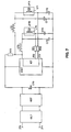
- the fourth exemplary embodiment of the invention shown in FIG. 4 has a mains voltage input with the mains voltage connections j40, j41, a filter and a mains voltage rectifier GL4, a downstream one Step-up converter HS4, one to the output of the step-up converter HS4 connected DC link capacitor C40, the supply voltage for an HW4 inverter.
- the inverter HW4 is a Load circuit designed as a resonance circuit which connects the resonance inductance L40, the capacitors C41, C42 and two electrical connections j42, j43 for the at least one induction coil L41 of an electrodeless one Discharge lamp LP4 has.
- the control of the inverter HW4 takes place with the help of a control circuit S4.
- the ignition capacitor C41 is connected in parallel to connections j42, j43.
- a connection of the Symmetry capacitor C42 is connected to the inverter HW4, while the other connection of the symmetry capacitor C42 over the Tap V40 is connected to the resonance inductor L40.
- the tap V40 is also connected to an input of the control circuit S4. additionally this circuit arrangement has an ohmic resistor R40, the one with the positive pole of the DC link capacitor C40 and on the other hand with a tap between the resonance inductance L40 and the connection j42 is connected in the load circuit.
- the control circuit S4 monitors the electrical potential at tap V40.
- the tap is located V40 at a comparatively high electrical potential, which essentially determined by the state of charge of the intermediate circuit capacitor C40 becomes.
- the tap V40 is connected to ground via the induction coil L41 connected and the tap V40 is therefore on a comparative low electrical potential.
- the control circuit S4 has one upstream monitoring element or integrated in the control circuit, For example, a logic circuit that the electrical potential at the tap V40 monitors and a corresponding digital or analog evaluation signal generated and fed to the control unit S4.
- the control circuit S4 is designed such that it starts the oscillation of the inverter HW4 only possible when the electrical potential at tap V40 is one predetermined, predetermined by the dimensioning of the circuit components Falls below value. This ensures that if there is no Lamp LP4 no ignition attempts have been made.
- the invention is not limited to the exemplary embodiments explained in more detail above.
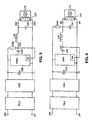
- the circuit arrangement of the fifth exemplary embodiment shown in FIG. 5 shows the application of the invention to a full bridge inverter.
- the circuit arrangement according to the fifth embodiment has, similar to that described in the first embodiment Mains voltage connection, a filter and a mains voltage rectifier and a step-up converter, which are not shown in FIG. 5.
- the one in figure 5 connections shown j50, j51 are at the output of the step-up converter connected so that the DC link capacitor C50 parallel to the output of the step-up converter is switched.
- the intermediate circuit capacitor C50 is one of the switching transistors Q1, Q2, Q3, Q4 and a control circuit (not shown) downstream full bridge inverter.
- the circuit arrangement has an ohmic resistor R50, the one with the positive pole of the DC link capacitor C50 and on the other hand is connected to a tap in the bridge branch, and a power line j54, which is the control circuit (not shown) of the full bridge inverter Q1, Q2, Q3, Q4 with another tap in the bridge branch combines.
- FIG. 6 shows the application of the invention to a free-swinging Half-bridge inverter according to a sixth embodiment.
- This circuit arrangement has, similar to the first embodiment described, a mains voltage connection, a filter and a Mains voltage rectifier and a step-up converter, which are not shown in FIG. 6 are shown.
- the connections j60, j61 shown in the figure are at the output of the step-up converter connected, so that the intermediate circuit capacitor C60 is connected in parallel to the output of the step-up converter.
- the DC link capacitor C60 is one of the two switching transistors Q5, Q6 half-bridge inverter formed downstream.
- Q6 is a resonant circuit trained load circuit connected which has a resonance inductance L60, an ignition capacitor C61, a symmetry capacitor C62 and two electrical connections j62 arranged in parallel with the ignition capacitor C61, j63 for at least one induction coil L61 of an electrodeless discharge lamp Has LP6.
- this circuit arrangement has an ohmic resistor R60, on the one hand to the positive pole of the DC link capacitor C60 and on the other hand to a tap in the load circuit, for example at the center tap between the two switching transistors Q5, Q6 is connected, and a power line j64, which is a second, located between the connection j63 and the symmetry capacitor Tapping in the load circuit with one input of the control circuit (not shown) of the half-bridge inverter Q5, Q6 connects.
- the control circuit of the half-bridge inverter Q5, Q6 comprises a transformer (not shown) with one connected to the load circuit of the half-bridge inverter Primary winding and two secondary windings, each connected to the Control electrode of one of the two switching transistors Q5, Q6 connected are, as well as a start circuit, with the help of a Diacs trigger pulses for the control electrode of the switching transistor Q6 generates the start-up of the half-bridge inverter.
- a free-swinging Half-bridge inverter with such a control circuit is, for example in the German patent application with the official file number 196 50110.5.
- the power line j64 is connected to the input of the start circuit. at missing discharge lamp LP6 becomes the symmetry capacitor C62 its very large capacity compared to the ignition capacitor C61 only insufficiently charged and the voltage drop across the symmetry capacitor C62 is therefore comparatively low. Hence the starting circuit Insufficient via the power line j64 when the discharge lamp LP6 is missing supplied with voltage so that the half-bridge inverter starts to oscillate not possible.
- FIGS. 7 to 13 show exemplary embodiments for circuit arrangements for operating two electrodeless discharge lamps.
- the circuit arrangement shown in Figure 7 according to the seventh embodiment has a line voltage input j70, j71, one to the line voltage input connected filter circuit with downstream Mains voltage rectifier GL7, one to the DC voltage output of the Rectifier GL7 connected to the step-up converter HS7, one parallel to the Output of the step-up converter HS7 arranged intermediate circuit capacitor C70 and an externally controlled half-bridge inverter HW7, whose Input is connected in parallel to the DC link capacitor C70.
- the half-bridge inverter HW7 is controlled by an integrated one Circuit IC7, which has its supply voltage through its connections j72 and j73 and the resistors R70, R71 and R72.
- HW7 half-bridge inverters To the HW7 half-bridge inverters are two resonance circuits connected in parallel trained load circuits connected, each with a resonance inductance L72 or L73, a resonance capacitor C71 or C73 and a further capacitor C72 or C74 and an electrodeless discharge lamp Have LP70 or LP71.
- the supply current for the integrated Circuit IC7 flows through both resonance inductors L72, L73 and via the induction coils L71 and L72 of the two electrodeless ones Discharge lamps LP70, LP71. Missing one of the discharge lamps LP70 or LP71, the integrated circuit IC7 is not supplied with voltage and the half-bridge inverter HW7 cannot start up.
- the eighth exemplary embodiment shown in FIG. 8 has a mains voltage input j80, j81, one connected to the mains voltage input Filter circuit with downstream mains voltage rectifier GL8, one connected to the DC voltage output of the rectifier GL8 Booster HS8, one parallel to the output of the booster HS8 arranged DC link capacitor C80 and an externally controlled Half-bridge inverter HW8, whose input is parallel to the DC link capacitor C80 is switched on.
- the control of the half-bridge inverter HW8 is implemented using an integrated circuit IC8, which has its supply voltage via its connections j82 and j83 and receives the resistors R80, R81, R82 and R83.
- the half-bridge inverter HW8 To the half-bridge inverter HW8 are two parallel circuits designed as resonance circuits Load circuits connected, each with a resonance inductance L82 or L83, a resonance capacitor C81 or C83 and another capacitor C82 or C84 and an electrodeless discharge lamp LP80 or Have LP81.
- the supply current for the IC8 integrated circuit flows here, not via the two resonance inductors L82, L83 as with seventh embodiment, but only via the induction coils L81 and L82 of the two electrodeless discharge lamps LP80, LP81. Is missing one of the discharge lamps LP80 or LP81, so the integrated circuit IC8 not supplied with voltage and the half-bridge inverter HW8 cannot start.
- the ninth embodiment of the invention shown in FIG. 9 has a mains voltage input with the mains voltage connections j90, j91, a filter and a mains voltage rectifier GL9, a downstream one Step-up converter HS9, one to the output of the step-up converter HS9 connected DC link capacitor C90, the supply voltage for an HW9 inverter.
- At the inverter HW9 are two load circuits connected in parallel, designed as resonance circuits, each have a resonance inductor L90 or L91, capacitors C91, C92 or C93, C94 and two electrical connections j92, j93 or j94, j95 for the at least one induction coil L92 or L93 of an electrodeless one Have discharge lamp LP90 or LP91.
- the control of the inverter HW9 takes place with the help of a control circuit S9.
- the ignition capacitors C93 and C94 are parallel to the respective connections j92, j93 or j94, j95 switched.
- a connection of the symmetrical capacitors C91 or C92 is connected to the inverter HW9 while you other connection via the tap V90 or V91 with the resonance inductance L90 or L91 is connected.
- this circuit arrangement two ohmic resistors R90, R91, each one with the positive pole of the DC link capacitor C90 and on the other hand with the tap V90 or V91 are connected in the respective load circuit.
- the Taps V90, V91 are also each with an input of the control circuit S9 connected.
- the control circuit S9 has an upstream or in the Control circuit integrated monitoring element, for example a logic Circuit that taps the electrical potential at the V90 and V91 monitors and a corresponding evaluation signal to the control unit S9 forwards. If there is no lamp at connections j92, j93 or j94, j95 LP90, LP91 is connected, the tap V90 or V91 is on a comparatively high electrical potential, which is essentially is determined by the state of charge of the intermediate circuit capacitor C90.
- the tap is V90 or V91 via the respective resonance inductance L90 or L91 and the corresponding induction coil L92 or L93 connected to earth and the tap V90 or V91 is located therefore at a comparatively low electrical potential.
- the monitoring link generates a the electrical potential at tap V90 or V91 corresponding digital or analog evaluation signal and leads this to the control circuit S9.
- the control circuit S9 is designed such that it only enables the HW9 inverter to start up if the electrical potential at the taps V90 and V91 unites predetermined, predetermined by the dimensioning of the circuit components Falls below value. This ensures that if there is no Lamp LP90 or LP91 no ignition attempts made.
- the tenth exemplary embodiment shown in FIG. 10 is largely correct with the ninth embodiment. How the Circuit arrangements of these two exemplary embodiments are identical. It were only the resistors R90, R91 by the equivalent resistors R90 'and R91', on the one hand with the positive connection of the intermediate circuit capacitor C90 and on the other hand with one between the resonance inductance and the lamp arranged in the respective load circuit tap connected, replaced. All other components match. Therefore the same reference numerals have been used in FIGS. 9 and 10 for identical components used.
- the circuit arrangement of the eleventh embodiment shown in FIG. 11 shows the application of the invention to a full bridge inverter for operating two electrodeless discharge lamps connected in parallel LP110, LP111.
- the circuit arrangement according to this embodiment has, similar to that described in the first embodiment, a mains voltage connection, a filter and a mains voltage rectifier and a step-up converter, which is not shown in FIG. 11 are.
- the connections j110, j111 shown in FIG. 11 are at the output of the step-up converter connected, so that the intermediate circuit capacitor C109 is connected in parallel to the output of the step-up converter.
- the DC link capacitor C109 is one of the switching transistors Q110, Q111, Q112, Q113 and a control circuit (not shown) existing Full bridge inverter connected downstream.
- the circuit arrangement has an ohmic resistance R110, which is arranged parallel to the switching path of transistor Q 110, and two power lines j116, 117 connecting the control circuit (not shown) of the full bridge inverter Q110, Q111, Q112, Q113 with one each Connect the tap in one of the bridge branches.
- Figure 12 shows, according to the twelfth embodiment, the application of the invention on a free-swinging half-bridge inverter for operating two electrodeless discharge lamps connected in parallel.
- This circuit arrangement has, similar to the first embodiment described, a mains voltage connection, a filter and a Mains voltage rectifier and a step-up converter, which are shown in FIG are not shown.
- the connections j120, j121 shown in FIG. 12 are on connected the output of the step-up converter, so that the intermediate circuit capacitor C120 is connected in parallel to the output of the step-up converter.
- the intermediate circuit capacitor C120 is one of the two switching transistors Q120, Q121 half-bridge inverter formed.
- this circuit arrangement has an ohmic resistor R120, which is connected to the positive pole of the intermediate circuit capacitor C120 and on the other hand to the Center tap connected between the two switching transistors Q120, Q121 and two power lines j126, j127, each between the connection j123 or j125 and the corresponding symmetry capacitor C122 or C124 tap in the respective load circuit with one input the control circuit (not shown) of the half-bridge inverter Connect Q120, Q121.
- the control circuit of the half-bridge inverter Q120, Q121 includes a transformer (not shown) with one in the Load circuit of the half-bridge inverter switched primary winding and two secondary windings, each connected to the control electrode of one of the two Switching transistors Q120, Q121 are connected, as well as a start circuit, which with the help of a diacs trigger pulses for the control electrode of the Switching transistor Q121 generates the oscillation of the half-bridge inverter to enable.
- a free-swinging half-bridge inverter with such a control circuit is, for example, in the German patent application with the official file number 196 50 110.5 described.
- the power lines j126, j127 are, for example via an AND circuit, connected to the input of the start circuit.
- One of the discharge lamps is missing LP122 or LP121, so becomes the corresponding symmetry capacitor C122 or C124 because of its compared to the ignition capacitor C121 or C123 very large capacity insufficiently charged and the Voltage drop across the respective symmetry capacitor C122 or C124 therefore comparatively small. Therefore, the start circuit via the Power lines j126 and j127 in the absence of a discharge lamp LP121 or LP122 insufficiently supplied with voltage so that it starts to vibrate of the half-bridge inverter is not possible.
- Figure 13 is a circuit arrangement according to the thirteenth embodiment the invention mapped to operate two in series switched electrodeless discharge lamps.
- the one shown in Figure 13 Circuit arrangement has a mains voltage input j130, j131, a filter circuit connected to the mains voltage input downstream mains voltage rectifier GL13, one to the DC voltage output of the rectifier GL13 connected step-up converter HS13, one arranged parallel to the output of the step-up converter HS13 DC link capacitor C130 and an externally controlled half-bridge inverter HW13, whose input is parallel to the DC link capacitor C70 is switched on.
- the control of the half-bridge inverter HW13 takes place by means of an integrated circuit IC13, which has its supply voltage via its connections j132 and j133.
- connection j133 is at ground potential, while the other terminal is connected in series switched induction coils L131, L132 of the electrodeless discharge lamps LP130 and LP131, the resonance inductor L130 and the ohmic resistor R130 to the positive connection of the intermediate circuit capacitor C130 is connected.
- One of the two is missing Lamps LP130 or LP131, so the aforementioned DC path is the connection j132 with the positive connection of the intermediate circuit capacitor C130 connecting, interrupted. In this case the integrated receives Circuit IC13 no supply voltage and the half-bridge inverter HW13 cannot start.
Landscapes
- Circuit Arrangements For Discharge Lamps (AREA)
Description
- Figur 1
- eine Schaltskizze des ersten Ausführungsbeispiels der Erfindung in schematischer Darstellung
- Figur 2
- eine Schaltskizze des zweiten Ausführungsbeispiels der Erfindung in schematischer Darstellung
- Figur 3
- eine Schaltskizze des dritten Ausführungsbeispiels der Erfindung in schematischer Darstellung
- Figur 4
- eine Schaltskizze des vierten Ausführungsbeispiels der Erfindung in schematischer Darstellung
- Figur 5
- eine Schaltskizze des fünften Ausführungsbeispiels der Erfindung in schematischer Darstellung
- Figur 6
- eine Schaltskizze des sechsten Ausführungsbeispiels der Erfindung in schematischer Darstellung
- Figur 7 bis 10
- schematische Schaltskizzen gemäß der Ausführungsbeispiele sieben bis zehn für zwei parallel geschaltete, an einem fremdgesteuerten Halbbrückenwechselrichter betriebene elektrodenlose Entladungslampen
- Figur 11
- eine schematische Schaltskizze gemäß des elften Ausführungsbeispiels für zwei parallel geschaltete, an einem Vollbrückenwechselrichter betriebene elektrodenlose Entladungslampen
- Figur 12
- eine schematische Schaltskizze gemäß des zwölften Ausführungsbeispiels für zwei parallel geschaltete, an einem freischwingenden Halbbrückenwechselrichter betriebene elektrodenlose Entladungslampen
- Figur 13
- eine schematische Schaltskizze gemäß des dreizehnten Ausführungsbeispiels für zwei in Reihe geschaltete, an einem Halbbbrückenwechselrichter betriebene elektrodenlose Entladungslampen
Claims (11)
- Schaltungsanordnung zum Betrieb mindestens einer elektrodenlosen Entladungslampe (LP1) mit mindestens einem Spannungseingang (j10, j11) zur Spannungsversorgung der Schaltungsanordnung und elektrischen Anschlüssen (j12, j13) für mindestens eine elektrodenlose Entladungslampe (LP1), wobeidadurch gekennzeichnet, dass wenigstens eine Induktionsspule (L11) der mindestens einen elektrodenlosen Entladungslampe (LP1), die das zur Zündung und Aufrechterhaltung einer Gasentladung in der Lampe (LP1) erforderliche elektrische Feld erzeugt, in dem Strompfad (C10, R10, j12, j13, IC1) angeordnet ist.die Schaltungsanordnung Kontrollmittel aufweist, die die Präsenz oder das Fehlen der mindestens einen elektrodenlosen Entladungslampe (LP1) an den elektrischen Anschlüssen feststellen (j12, j13) und die das Bereitstellen der Zünd- und/oder Betriebsspannung für die mindestens eine elektrodenlose Entladungslampe (LP1) erst dann ermöglichen, wenn die mindestens eine elektrodenlose Entladungslampe (LP1) an die elektrischen Anschlüsse (j12, j13) angeschlossen ist,die Kontrollmittel einen Strompfad (C10, R10, j12, j13, IC1) und einen Strom- oder Spannungsdetektor (IC1) aufweisen, wobeider Strompfad (C10, R10, j12, j 13, IC1) einen ersten elektrischen Widerstandswert besitzt, wenn die mindestens eine Entladungslampe (LP1) an die Schaltungsanordnung angeschlossen ist,der Strompfad (C10, R10, j12, j13, IC1) einen anderen elektrischen Widerstandswert besitzt, wenn keine Entladungslampe an die Schaltungsanordnung angeschlossen ist,der Strom- oder Spannungsdetektor (IC1) den Stromfluß oder den Spannungsabfall in dem Strompfad (C10, R10, j12, j13, IC1) überwacht,
- Schaltungsanordnung nach Anspruch 1, dadurch gekennzeichnet, daß die Schaltungsanordnung mindestens einen Spannungswandler (HW1) und eine Steuerschaltung (IC1) für den mindestens einen Spannungswandler (HW1) sowie einen, dem mindestens einen Spannungswandler (HW1) nachgeschalteten Lastkreis besitzt, wobei die Kontrollmittel mit der Steuerschaltung (IC1) derart zusammenwirken, daß die Steuerschaltung (IC1) nur dann Ansteuerungsimpulse für den mindestens einen Spannungswandler (HW1) generiert, wenn die mindestens eine elektrodenlose Entladungslampe (LP1) an die elektrischen Anschlüsse (j12, j13) angeschlossen ist.
- Schaltungsanordnung nach Anspruch 2, dadurch gekennzeichnet, daß die Kontrollmittel ein Überwachungsglied (S3) und einen Abgriff im Lastkreis (V30) umfassen, wobeidas elektrische Potential an dem Abgriff (V30) einen ersten Wert besitzt, wenn die mindestens eine Entladungslampe (LP3) an die Schaltungsanordnung angeschlossen ist, und einen zweiten, anderen Wert besitzt, wenn keine Entladungslampe an die Schaltungsanordnung angeschlossen ist, unddas Überwachungsglied (S3) das elektrische Potential an dem Abgriff (V30) überwacht und ein dem elektrischen Potential entsprechendes Auswertungssignal für die Steuerschaltung (S3) erzeugt.
- Schaltungsanordnung nach Anspruch 2, dadurch gekennzeichnet, daß die Steuerschaltung (IC1) als Integrierter Schaltkreis ausgebildet ist.
- Schaltungsanordnung nach den Ansprüchen 2 und 4, dadurch gekennzeichnet, daß die Kontrollmittel als ein an einen Spannungsversorgungsanschluß (j14) des Integrierten Schaltkreises (IC1) angeschlossenen Strompfad (C10, R10, j12, j13, IC1) ausgebildet sind, der beim Fehlen der mindestens einen elektrodenlosen Entladungslampe (LP1) an den elektrischen Anschlüssen (j12, j13) unterbrochen ist.
- Schaltungsanordnung nach Anspruch 1, dadurch gekennzeichnet, daß der Strompfad (C10, R10, j12, j13, IC1) ein Gleichstrompfad ist.
- Schaltungsanordnung nach Anspruch 1, dadurch gekennzeichnet, daß der Strompfad (C10, R10, j12, j13, IC1) unterbrochen ist, wenn keine Entladungslampe an die Schaltungsanordnung angeschlossen ist.
- Schaltungsanordnung nach Anspruch 1, dadurch gekennzeichnet, daß die elektrischen Anschlüsse (j12, j13) für die mindestens eine elektrodenlose Entladungslampe (LP1) in dem Strompfad (C10, R10, j12, j13, IC1) angeordnet sind.
- Schaltungsanordnung nach Anspruch 2 oder 4, dadurch gekennzeichnet, daß der mindestens eine Spannungswandler (HW1) ein Wechselrichter ist und der Lastkreis als Resonanzkreis ausgebildet ist.
- Schaltungsanordnung nach den Ansprüchen 1 und 4, dadurch gekennzeichnet, daß der Strompfad (C 10, R10, j12, j13, IC1) an einen Spannungsversorgungsanschluß (j14) des Integrierten Schaltkreises (IC1) angeschlossen ist und der Strom- oder Spannungsdetektor der Integrierte Schaltkreis (IC1) ist.
- Schaltungsanordnung nach den Ansprüchen 1 und 4, dadurch gekennzeichnet, daß der Strompfad (C10, R10, j12, j13, IC1) Bestandteil eines Stromversorgungspfades des Integrierten Schaltkreises (IC1) ist und der Strom- oder Spannungsdetektor der Integrierte Schaltkreis (IC1) ist.
Applications Claiming Priority (3)
| Application Number | Priority Date | Filing Date | Title |
|---|---|---|---|
| DE19805314A DE19805314A1 (de) | 1998-02-10 | 1998-02-10 | Schaltungsanordnung zum Betrieb mindestens einer elektrodenlosen Entladungslampe |
| DE19805314 | 1998-02-10 | ||
| PCT/DE1999/000196 WO1999041954A1 (de) | 1998-02-10 | 1999-01-27 | Schaltungsanordnung zum betrieb mindestens einer elektrodenlosen entladungslampe |
Publications (2)
| Publication Number | Publication Date |
|---|---|
| EP0974247A1 EP0974247A1 (de) | 2000-01-26 |
| EP0974247B1 true EP0974247B1 (de) | 2004-03-24 |
Family
ID=7857218
Family Applications (1)
| Application Number | Title | Priority Date | Filing Date |
|---|---|---|---|
| EP99907281A Expired - Lifetime EP0974247B1 (de) | 1998-02-10 | 1999-01-27 | Schaltungsanordnung zum betrieb mindestens einer elektrodenlosen entladungslampe |
Country Status (8)
| Country | Link |
|---|---|
| US (1) | US6181080B1 (de) |
| EP (1) | EP0974247B1 (de) |
| JP (1) | JP2001522524A (de) |
| AT (1) | ATE262772T1 (de) |
| CA (1) | CA2286139A1 (de) |
| DE (2) | DE19805314A1 (de) |
| ES (1) | ES2218998T3 (de) |
| WO (1) | WO1999041954A1 (de) |
Families Citing this family (12)
| Publication number | Priority date | Publication date | Assignee | Title |
|---|---|---|---|---|
| US6532070B1 (en) * | 2000-07-17 | 2003-03-11 | Therma-Wave, Inc. | Method for determining ion concentration and energy of shallow junction implants |
| AU2001280708A1 (en) | 2000-07-21 | 2002-02-05 | Osram Sylvania Inc. | Method and apparatus for arc detection and protection for electronic ballasts |
| WO2002017798A1 (de) * | 2000-08-31 | 2002-03-07 | Plus Endoprothetik Ag | Verfahren und anordnung zur ermittlung einer belastungsachse einer extremität |
| JP2002100493A (ja) * | 2000-09-26 | 2002-04-05 | Toshiba Lighting & Technology Corp | 無電極放電灯装置 |
| DE10160790A1 (de) * | 2001-01-12 | 2002-08-08 | Patent Treuhand Ges Fuer Elektrische Gluehlampen Mbh | Schaltungsanordnung zum Einschalten einer Teilschaltungsanordnung |
| EP1227706B1 (de) * | 2001-01-24 | 2012-11-28 | City University of Hong Kong | Neue Schaltungsentwürfe und Steuerungstechniken für elektronische Hochfrequenz-Vorschaltgeräte für Entladungslampen hoher Intensität |
| US6459210B1 (en) * | 2001-03-01 | 2002-10-01 | Toko, Inc. | Switch mode energy recovery for electro-luminescent lamp panels |
| DE10306793A1 (de) * | 2002-05-21 | 2003-12-04 | Plus Endoprothetik Ag Rotkreuz | Anordnung und Verfahren zur intraoperativen Festlegung der Lage eines Gelenkersatzimplantats |
| JP2007265902A (ja) * | 2006-03-29 | 2007-10-11 | Matsushita Electric Ind Co Ltd | 無電極放電灯装置、およびそれを用いた照明器具 |
| TWI418248B (zh) * | 2010-05-27 | 2013-12-01 | I Mag Electronic Corp | 無極燈高頻發生器之延遲啟動電路及使用其之高頻發生器 |
| CN102762019B (zh) * | 2011-04-28 | 2014-08-13 | 广东格林莱光电科技有限公司 | 一种hid电子镇流电路、电子镇流器及高压气体放电灯 |
| TW201438521A (zh) * | 2013-03-19 | 2014-10-01 | Nuopo Energy Saving Optronics Corp | 一種低頻無極節能燈 |
Family Cites Families (10)
| Publication number | Priority date | Publication date | Assignee | Title |
|---|---|---|---|---|
| US4245178A (en) | 1979-02-21 | 1981-01-13 | Westinghouse Electric Corp. | High-frequency electrodeless discharge device energized by compact RF oscillator operating in class E mode |
| GB8508913D0 (en) | 1985-04-04 | 1985-05-09 | Lee C T | Electronic ballast |
| US5063332A (en) * | 1990-12-21 | 1991-11-05 | General Electric Company | Feedback control system for a high-efficiency class-D power amplifier circuit |
| JPH0521182A (ja) * | 1990-12-30 | 1993-01-29 | Toshiba Lighting & Technol Corp | 放電灯点灯装置および照明器具 |
| US5574336A (en) | 1995-03-28 | 1996-11-12 | Motorola, Inc. | Flourescent lamp circuit employing a reset transistor coupled to a start-up circuit that in turn controls a control circuit |
| JP3210561B2 (ja) * | 1995-06-14 | 2001-09-17 | 株式会社小糸製作所 | 放電灯点灯回路 |
| US5834905A (en) | 1995-09-15 | 1998-11-10 | Osram Sylvania Inc. | High intensity electrodeless low pressure light source driven by a transformer core arrangement |
| GB2305311A (en) | 1995-09-18 | 1997-04-02 | Gen Electric | Self oscillating drive circuit for an electrodeless discharge lamp |
| JP3280567B2 (ja) * | 1996-04-04 | 2002-05-13 | 株式会社小糸製作所 | 放電灯点灯回路 |
| DE19650110A1 (de) | 1996-12-03 | 1998-06-04 | Patent Treuhand Ges Fuer Elektrische Gluehlampen Mbh | Betriebsschaltung für eine elektrodenlose Niederdruckentladungslampe |
-
1998
- 1998-02-10 DE DE19805314A patent/DE19805314A1/de not_active Withdrawn
-
1999
- 1999-01-27 US US09/381,343 patent/US6181080B1/en not_active Expired - Lifetime
- 1999-01-27 AT AT99907281T patent/ATE262772T1/de active
- 1999-01-27 WO PCT/DE1999/000196 patent/WO1999041954A1/de not_active Ceased
- 1999-01-27 ES ES99907281T patent/ES2218998T3/es not_active Expired - Lifetime
- 1999-01-27 CA CA002286139A patent/CA2286139A1/en not_active Abandoned
- 1999-01-27 JP JP54089099A patent/JP2001522524A/ja active Pending
- 1999-01-27 DE DE59908932T patent/DE59908932D1/de not_active Expired - Lifetime
- 1999-01-27 EP EP99907281A patent/EP0974247B1/de not_active Expired - Lifetime
Also Published As
| Publication number | Publication date |
|---|---|
| DE59908932D1 (de) | 2004-04-29 |
| US6181080B1 (en) | 2001-01-30 |
| ES2218998T3 (es) | 2004-11-16 |
| EP0974247A1 (de) | 2000-01-26 |
| JP2001522524A (ja) | 2001-11-13 |
| ATE262772T1 (de) | 2004-04-15 |
| WO1999041954A1 (de) | 1999-08-19 |
| DE19805314A1 (de) | 1999-08-19 |
| CA2286139A1 (en) | 1999-08-19 |
Similar Documents
| Publication | Publication Date | Title |
|---|---|---|
| EP0974247B1 (de) | Schaltungsanordnung zum betrieb mindestens einer elektrodenlosen entladungslampe | |
| EP0708579B1 (de) | Verfahren zum Betrieb einer Entladungslampe und Schaltungsanordnung zum Betrieb einer Entladungslampe | |
| EP1286572B1 (de) | Vorschaltgerät zum Betrieb mindestens einer Niederdruckentladungslampe | |
| EP1333707A1 (de) | Elektronisches Vorschaltgerät für Gasentladungslampe | |
| EP0439240B1 (de) | Elektronisches Vorschaltgerät | |
| DE3829388A1 (de) | Schaltungsanordnung zum betrieb einer last | |
| DE19843643B4 (de) | Schaltungsanordnung zum Starten und Betreiben einer Hochdruck-Entladungslampe | |
| DE102005007346A1 (de) | Schaltungsanordnung und Verfahren zum Betreiben von Gasentladungslampen | |
| DE69029301T2 (de) | Anzündanordnung für eine entladungslampe | |
| DE3301108A1 (de) | Verfahren zum betreiben einer gasentladungslampe | |
| DE69928445T2 (de) | Digitale leistungssteuerung | |
| DE69713480T2 (de) | Schaltungsanordnung | |
| EP1729546B1 (de) | Elektronisches Vorschaltgerät für mindestens eine Lampe | |
| DE102006018577A1 (de) | Hochsetzsteller-Leistungsfaktorkorrekturschaltung (Boost-PFC) | |
| DE60111563T2 (de) | Vorrichtung zur gewährleistung eines überlastschutzes für eine schaltung | |
| EP1326484B1 (de) | Betriebsgerät für Gasentladungslampen | |
| DE10206175B4 (de) | Schaltung zum Betreiben einer Entladungslampe | |
| EP0642295B1 (de) | Elektronisches Vorschaltgerät zum Versorgen einer Last, beispielsweise einer Lampe | |
| EP1696713B1 (de) | EVG für Hochdruckentladungslampe mit Strommesseinrichtung | |
| EP1589645A2 (de) | Schaltung zum Umwandeln einer Wechselspannung in eine Gleichspannung | |
| EP1651014A1 (de) | Lampenbetriebsschaltung und Betriebsverfahren für eine Lampe mit Wirkstrommessung | |
| DE69714163T2 (de) | Schaltungsanordnung | |
| DE102004017479A1 (de) | EVG mit Resonanzanregung zur Übernahmespannungserzeugung | |
| EP0949851B1 (de) | Schaltungsanordnung zum Betrieb von Niederdruckentladungslampen | |
| DE10102837A1 (de) | Betriebsgerät für Gasentladungslampen mit Abschaltung der Wendelheizung |
Legal Events
| Date | Code | Title | Description |
|---|---|---|---|
| PUAI | Public reference made under article 153(3) epc to a published international application that has entered the european phase |
Free format text: ORIGINAL CODE: 0009012 |
|
| 17P | Request for examination filed |
Effective date: 19991005 |
|
| AK | Designated contracting states |
Kind code of ref document: A1 Designated state(s): AT BE CH DE ES FR GB IT LI NL SE |
|
| 17Q | First examination report despatched |
Effective date: 20021122 |
|
| GRAP | Despatch of communication of intention to grant a patent |
Free format text: ORIGINAL CODE: EPIDOSNIGR1 |
|
| RTI1 | Title (correction) |
Free format text: CIRCUIT FOR ACTUATING AT LEAST ONE ELECTRODELESS DISCHARGE LAMP |
|
| RTI1 | Title (correction) |
Free format text: CIRCUIT FOR ACTUATING AT LEAST ONE ELECTRODELESS DISCHARGE LAMP |
|
| GRAS | Grant fee paid |
Free format text: ORIGINAL CODE: EPIDOSNIGR3 |
|
| GRAA | (expected) grant |
Free format text: ORIGINAL CODE: 0009210 |
|
| AK | Designated contracting states |
Kind code of ref document: B1 Designated state(s): AT BE CH DE ES FR GB IT LI NL SE |
|
| REG | Reference to a national code |
Ref country code: GB Ref legal event code: FG4D Free format text: NOT ENGLISH |
|
| REG | Reference to a national code |
Ref country code: CH Ref legal event code: NV Representative=s name: SIEMENS SCHWEIZ AG Ref country code: CH Ref legal event code: EP |
|
| REF | Corresponds to: |
Ref document number: 59908932 Country of ref document: DE Date of ref document: 20040429 Kind code of ref document: P |
|
| REG | Reference to a national code |
Ref country code: SE Ref legal event code: TRGR |
|
| GBT | Gb: translation of ep patent filed (gb section 77(6)(a)/1977) |
Effective date: 20040602 |
|
| REG | Reference to a national code |
Ref country code: ES Ref legal event code: FG2A Ref document number: 2218998 Country of ref document: ES Kind code of ref document: T3 |
|
| ET | Fr: translation filed | ||
| PLBE | No opposition filed within time limit |
Free format text: ORIGINAL CODE: 0009261 |
|
| STAA | Information on the status of an ep patent application or granted ep patent |
Free format text: STATUS: NO OPPOSITION FILED WITHIN TIME LIMIT |
|
| 26N | No opposition filed |
Effective date: 20041228 |
|
| PGFP | Annual fee paid to national office [announced via postgrant information from national office to epo] |
Ref country code: NL Payment date: 20060104 Year of fee payment: 8 |
|
| PGFP | Annual fee paid to national office [announced via postgrant information from national office to epo] |
Ref country code: SE Payment date: 20060105 Year of fee payment: 8 |
|
| PGFP | Annual fee paid to national office [announced via postgrant information from national office to epo] |
Ref country code: BE Payment date: 20060112 Year of fee payment: 8 |
|
| PGFP | Annual fee paid to national office [announced via postgrant information from national office to epo] |
Ref country code: ES Payment date: 20060209 Year of fee payment: 8 |
|
| PG25 | Lapsed in a contracting state [announced via postgrant information from national office to epo] |
Ref country code: SE Free format text: LAPSE BECAUSE OF NON-PAYMENT OF DUE FEES Effective date: 20070128 |
|
| EUG | Se: european patent has lapsed | ||
| NLV4 | Nl: lapsed or anulled due to non-payment of the annual fee |
Effective date: 20070801 |
|
| BERE | Be: lapsed |
Owner name: *PATENT-TREUHAND-G.- FUR ELEKTRISCHE GLUHLAMPEN M. Effective date: 20070131 |
|
| PG25 | Lapsed in a contracting state [announced via postgrant information from national office to epo] |
Ref country code: BE Free format text: LAPSE BECAUSE OF NON-PAYMENT OF DUE FEES Effective date: 20070131 |
|
| PG25 | Lapsed in a contracting state [announced via postgrant information from national office to epo] |
Ref country code: NL Free format text: LAPSE BECAUSE OF NON-PAYMENT OF DUE FEES Effective date: 20070801 |
|
| REG | Reference to a national code |
Ref country code: ES Ref legal event code: FD2A Effective date: 20070129 |
|
| PG25 | Lapsed in a contracting state [announced via postgrant information from national office to epo] |
Ref country code: ES Free format text: LAPSE BECAUSE OF NON-PAYMENT OF DUE FEES Effective date: 20070129 |
|
| REG | Reference to a national code |
Ref country code: CH Ref legal event code: PCAR Free format text: SIEMENS SCHWEIZ AG;INTELLECTUAL PROPERTY FREILAGERSTRASSE 40;8047 ZUERICH (CH) |
|
| PGFP | Annual fee paid to national office [announced via postgrant information from national office to epo] |
Ref country code: IT Payment date: 20110126 Year of fee payment: 13 Ref country code: AT Payment date: 20101209 Year of fee payment: 13 |
|
| PGFP | Annual fee paid to national office [announced via postgrant information from national office to epo] |
Ref country code: CH Payment date: 20110407 Year of fee payment: 13 |
|
| REG | Reference to a national code |
Ref country code: DE Ref legal event code: R081 Ref document number: 59908932 Country of ref document: DE Owner name: OSRAM GMBH, DE Free format text: FORMER OWNER: OSRAM GESELLSCHAFT MIT BESCHRAENKTER HAFTUNG, 81543 MUENCHEN, DE Effective date: 20111130 |
|
| REG | Reference to a national code |
Ref country code: CH Ref legal event code: PL |
|
| PG25 | Lapsed in a contracting state [announced via postgrant information from national office to epo] |
Ref country code: CH Free format text: LAPSE BECAUSE OF NON-PAYMENT OF DUE FEES Effective date: 20120131 Ref country code: LI Free format text: LAPSE BECAUSE OF NON-PAYMENT OF DUE FEES Effective date: 20120131 |
|
| PG25 | Lapsed in a contracting state [announced via postgrant information from national office to epo] |
Ref country code: IT Free format text: LAPSE BECAUSE OF NON-PAYMENT OF DUE FEES Effective date: 20120127 |
|
| REG | Reference to a national code |
Ref country code: AT Ref legal event code: MM01 Ref document number: 262772 Country of ref document: AT Kind code of ref document: T Effective date: 20120127 |
|
| PG25 | Lapsed in a contracting state [announced via postgrant information from national office to epo] |
Ref country code: AT Free format text: LAPSE BECAUSE OF NON-PAYMENT OF DUE FEES Effective date: 20120127 |
|
| REG | Reference to a national code |
Ref country code: DE Ref legal event code: R081 Ref document number: 59908932 Country of ref document: DE Owner name: OSRAM GMBH, DE Free format text: FORMER OWNER: OSRAM AG, 81543 MUENCHEN, DE Effective date: 20130205 |
|
| REG | Reference to a national code |
Ref country code: DE Ref legal event code: R081 Ref document number: 59908932 Country of ref document: DE Owner name: OSRAM GMBH, DE Free format text: FORMER OWNER: OSRAM GMBH, 81543 MUENCHEN, DE Effective date: 20130822 |
|
| PGFP | Annual fee paid to national office [announced via postgrant information from national office to epo] |
Ref country code: FR Payment date: 20140123 Year of fee payment: 16 |
|
| PGFP | Annual fee paid to national office [announced via postgrant information from national office to epo] |
Ref country code: GB Payment date: 20140121 Year of fee payment: 16 |
|
| PGFP | Annual fee paid to national office [announced via postgrant information from national office to epo] |
Ref country code: DE Payment date: 20150121 Year of fee payment: 17 |
|
| GBPC | Gb: european patent ceased through non-payment of renewal fee |
Effective date: 20150127 |
|
| PG25 | Lapsed in a contracting state [announced via postgrant information from national office to epo] |
Ref country code: GB Free format text: LAPSE BECAUSE OF NON-PAYMENT OF DUE FEES Effective date: 20150127 |
|
| REG | Reference to a national code |
Ref country code: FR Ref legal event code: ST Effective date: 20150930 |
|
| PG25 | Lapsed in a contracting state [announced via postgrant information from national office to epo] |
Ref country code: FR Free format text: LAPSE BECAUSE OF NON-PAYMENT OF DUE FEES Effective date: 20150202 |
|
| REG | Reference to a national code |
Ref country code: DE Ref legal event code: R119 Ref document number: 59908932 Country of ref document: DE |
|
| PG25 | Lapsed in a contracting state [announced via postgrant information from national office to epo] |
Ref country code: DE Free format text: LAPSE BECAUSE OF NON-PAYMENT OF DUE FEES Effective date: 20160802 |