EP0972300B1 - Verfahren zur herstellung von integrierten schaltungen - Google Patents
Verfahren zur herstellung von integrierten schaltungen Download PDFInfo
- Publication number
- EP0972300B1 EP0972300B1 EP99900602A EP99900602A EP0972300B1 EP 0972300 B1 EP0972300 B1 EP 0972300B1 EP 99900602 A EP99900602 A EP 99900602A EP 99900602 A EP99900602 A EP 99900602A EP 0972300 B1 EP0972300 B1 EP 0972300B1
- Authority
- EP
- European Patent Office
- Prior art keywords
- defects
- wafer
- stage
- class
- processing
- Prior art date
- Legal status (The legal status is an assumption and is not a legal conclusion. Google has not performed a legal analysis and makes no representation as to the accuracy of the status listed.)
- Expired - Lifetime
Links
Images

Classifications
-
- H—ELECTRICITY
- H01—ELECTRIC ELEMENTS
- H01L—SEMICONDUCTOR DEVICES NOT COVERED BY CLASS H10
- H01L21/00—Processes or apparatus adapted for the manufacture or treatment of semiconductor or solid state devices or of parts thereof
- H01L21/67—Apparatus specially adapted for handling semiconductor or electric solid state devices during manufacture or treatment thereof; Apparatus specially adapted for handling wafers during manufacture or treatment of semiconductor or electric solid state devices or components ; Apparatus not specifically provided for elsewhere
- H01L21/67005—Apparatus not specifically provided for elsewhere
- H01L21/67242—Apparatus for monitoring, sorting or marking
- H01L21/67288—Monitoring of warpage, curvature, damage, defects or the like
-
- H—ELECTRICITY
- H01—ELECTRIC ELEMENTS
- H01L—SEMICONDUCTOR DEVICES NOT COVERED BY CLASS H10
- H01L22/00—Testing or measuring during manufacture or treatment; Reliability measurements, i.e. testing of parts without further processing to modify the parts as such; Structural arrangements therefor
- H01L22/20—Sequence of activities consisting of a plurality of measurements, corrections, marking or sorting steps
Definitions
- the invention relates to a method of manufacturing integrated circuits as described in the precharacterizing part of claim 1.
- Integrated circuits are manufactured by submitting wafers to a series of processing steps. During processing defects may occur on the wafer, which reduce the yield of properly functioning integrating circuits on the wafer. Malfunctioning apparatuses may increase the number of defects.
- the abstract of Japanese patent application laid open number 5-259015 (1993) proposes to count the number of defects such as particles or patterning errors on the wafer after a processing step. If the number of defects is to high, it is attempted to redo the processing step in order to remove the defects. If this is not possible, the wafer is discarded and the process conditions are adjusted before processing further wafers.
- Such a method may be used in factory management system to increase the yield and to control the correction of malfunctioning apparatuses.
- the factory management system would become very expensive, even if it were possible without disturbing the processing steps.
- the defects might be due to apparatuses that perform earlier processing steps.
- Appatuses generally refer to devices that have an individual effect on integrated circuit wafers at some stage; as used herein, an apparatus may be a component of a system containing several such components.
- processing steps refer generally to tasks performed by the apparatuses.
- Examples of different classes of defects that can be distinguished are scratches, particle contamination, lattice stacking faults, dripped liquid, focus errors, pinholes in patterns, bridges between patterns, poorly developed patterns, deviating linewidths, presence of flakes, Tungsten particles, Ti/TiN particles, Blocked etch, corrosion, missing contacts etc.
- Claim 2 Another embodiment of the method according to the invention is described in Claim 2.
- This embodiment provides for using a differential count, representing the increase in the number of defects due to a number of processing steps between defect counting at a first stage and defect counting at a second stage.
- the differential count is much more sensitive to defects caused by apparatuses performing processing steps between the second and first stage, and therefore apparatuses can be switched off-line more reliably.
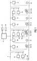
- Figure 1 shows an illustrative example of an automated integrated circuit manufacturing system.
- the system comprises a central computer 10, with memory units 101, 102, handling stations 14a-i and a network 12 connecting the central computer 10 to the handling station 14a-i. Batches of wafers 16a-n waiting to be processed at the handling stations 14a-i are shown symbolically.
- a transport system 18 is shown for transporting batches 16a-n between handling stations 14a-i.
- the integrated circuit manufacturing system ensures that wafers undergo a series of processing steps to manufacture a desired integrated circuit.
- FIG. 2 shows an example of part of a flow chart of an integrated circuit manufacturing process.
- the flow-chart contains a number of processing steps 20a-i which performed sequentially upon the wafer. Examples of processing steps include deposition of photo-resist, exposure of the resist using a photo-mask, resist developing, etching, implantation, material deposition from liquids, vapors, gasses and many others.
- the flow-chart also shows two visual inspection steps 22, 24, to be executed between different processing steps.
- Different processing steps are generally executed by different handling stations 14a-i, which contain apparatuses for performing specific types of processing steps.
- apparatuses include for example wafer steppers, etchers, developers, implantation apparatuses, deposition equipment and many others.
- Dependent on the type of apparatus there may be one or more equivalent apparatuses available to perform the same processing step.
- Figure 1 illustrates this by showing different handling stations 14a-i for equivalent apparatuses vertically below one another.
- Each wafer or batch of wafers 16a-n has an identity which is represented in the central computer 10.
- the central computer 10 stores information about the process flow-chart that a wafer or batch of wafers 16a-n should undergo. This information defines the processing steps 20a-i that have to be performed and their sequence.
- the central computer also records which processing steps 20a-i have already been performed on a wafer or batch of wafers 16a-n and determines what next processing step 20a-i should be performed on a wafer or a batch of wafers 16a-n.
- the central computer 10 sends signals via the network 12 to the handling stations 14a-i or the transport system in order to ensure that the batches or wafers are transported to a handling station 14a-i capable of performing that next processing step 20a-i.
- the transport may be effected by the transport system 18 or by a human operator.
- the identity of the wafers or the batch 16a-n is signaled by the handling station 14a-i to the central computer 10.
- the central computer checks whether the flow-chart prescribes that the identified wafer or batch 16a-n should undergo next the particular processing step for which the handling station 14a-i is used. If this is not so the central computer 10 sends an error signal to the handling station 14a-i in order to prevent processing of that wafer or batch 16a-n at that handling station 14a-i.
- the handling station 14a-i responds to this signal for example by refusing to load the wafer or batch 16a-n or by displaying an error report to a human operator which signaled the intent to process the wafer o batch 16a-n at the handling station 14a-i.
- the central computer 10 indicates the next handling station 14a-i or group of equivalent handling stations 14a-i to which the wafer or batch 16a-n should be transported.
- defect detection systems can be used for detecting defects.
- visual inspection stations are provided for performing visual inspection steps 22, 24 of wafers once they have undergone a number of processing steps 20a-i.
- the defects detected are applied to control the use of the handling stations 14a-i.
- classes of defects with different types of visual appearance. Examples of classes are scratches, presence of contaminating particles, lattice stacking faults, dripped liquid, focus errors, pinholes in patterns, bridges between patterns, poorly developed patterns, deviating linewidths, presence of flakes, Tungsten particles, Ti/TiN particles, blocked etch, signs of corrosion, missing contacts etc.
- the defects may be classified by a person or automatically, e.g. using a visual pattern recognition system.
- Figure 3a-b show examples of defects from different classes.
- Figure 3a shows an image of an integrated circuit which contains an image feature 40 which is not normally present in images of the integrated circuit.
- the image feature 40 is assigned to a class of defects containing features that are characterized by features having irregular shape with sharp corners. This class is associated with etchers (and is labeled blocked etch defect). When the density of defects from this class exceeds its control limit the etcher which produces the relevant layer is switched off-line.
- Figure 3b shows an image of an integrated circuit in which contacts (visible as dots) 42a, 44a are missing at locations 42b, 44b on the right side of the image, where they should occur in normal circuits.
- Such an image is classified into a class of defects which are characterized by missing contacts. This class is associated for example with an oxide etcher. When the density of defects from this class exceeds its control limit, the oxide etcher which was used to process the integrated circuit is switched off-line.
- each class associates with one or more apparatus types used in specific processing steps 20a-i.
- a class is associated with a processing step this implies that the apparatus used in the associated processing step 20a-i may cause defects in that class when the apparatus performing the processing step 20a-i does not function properly.
- Examples of associations are scratches- all apparatuses in all steps presence of many different types of particles - all apparatuses in all steps repeating defect - reticle in exposure step poor focus - lithographic exposure system in lithography steps pinhole defect - apparatus used in application of resist step bridging defect - apparatus used in application of resist step poor development - apparatus used in developing step deviating linewidth - apparatus used in litho steps presence of flakes - etching, CVD (Chemical vapor deposition) SOG blocked etch - etchers, Litho equipment corrosion - etching, resist stripping polymer flakes- polymer forming etch equipment
- the count of the number of defects is applied to control the use of apparatuses.
- This function is performed for example by the central computer 10.
- a control limit is defined indicating a number of defects in that defect class that is acceptable at the stage in the process where the defects are detected.
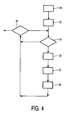
- Figure 4 shows a flow-chart for controlling use of the handling stations 14a-i by means of the detected defects.
- a first step 30 defects are detected visually and there position is noted.
- the detected defects are classified into classes of defects types with different visual appearance. A count is kept of the number of defects in each class.
- the subsequent steps 34, 36, 37, 38, 39 are performed for each of the classes. For this purpose, an actual class is initialized to an initial class in the second step 32.
- a third step 34 the count of the number of defects in the actual class is compared to a control limit defined for that class. If the number of defects in the class exceeds the control limit, a fourth step 36 is executed, which determines the processing steps 20a-i that are associated with the actual class. In a fifth step 37 it is determined which apparatuses performed those processing steps on the inspected wafer and are of the type associated with the defect class. These apparatuses are then switched off-line in a sixth step 38. In a seventh step 39 it is determined whether all classes have been considered. This step is also entered from the third step if the count of defects of the actual class is below the control limit. If there remain classes that have not been considered, the flow-chart is repeated from the third step for one of the remaining classes.
- the visual inspection is used to measure the performance of the processing apparatuses included in the handling stations 14a-i, not to detect all individual faulty chips. Therefore, it is sufficient to take samples instead of inspecting all wafers or all defects. For example, one might inspect only a fraction of the wafers, or only part of the area on the wafers that are inspected. Similarly, one might classify only a sample of all defects. All such sampled inspection can be converted into estimated defect densities per unit area on all wafers.
- defects on the wafers are detected and classified into different classes in two steps. This may be realized for example by comparing the image of one chip on the wafer with another chip on the wafer. If the difference is too great at a certain location on a chip, a defect and the corresponding position are reported. The locations for which defects are reported are subsequently analyzed in more detail to classify the defect.
- the classification may be realized by showing an image of an area of the chip surrounding the location to a human operator, and receiving from the human operator a classification code of the class recognized by the human operator. Alternatively, automatic visual classification equipment may be used.
- one does not count individual defect locations, but only clusters of spatially close defect locations. Thus it can be prevented that apparatuses are switched of due do a few local defects with many defect locations.
- Visual inspection steps may take place at more than one different stage during processing.
- visual inspection takes place at a stage between steps 20b and 20c and at a later stage between steps 20f and 20g.
- the processing steps that are associated with different defect classes will depend on the stage at which the visual inspection takes place. Usually, only a number of the last preceding steps 20a-i before the stage of the visual inspection step 22, 24 will be associated with any defect class, but no earlier processing steps 20a-i.
- defects from distant earlier processing steps 20a-i will still be visible at a stage where an inspection step 22, 24 takes place. This may affect the reliability with which the count of the number of defects in a class may be used to take apparatuses off-line. To reduce this problem, one may discount defects that have been caused by such distant earlier processing steps.
- a preferred way of doing this is to keep a record of the locations on a wafer at which defects have been detected at an earlier stage and to count defects on that wafer at a later stage only if those defects are not located at or near locations where defects have been detected at an earlier stage (or at least where defects in related classes have been detected at the earlier stage; a first and second class are said to be related if it is known that defects from the first class after a first step often precede defects from the second class after a later step).
- Nai is the counts of defects in the ith class at stage "a” and pred(Nbi) is the prediction of the count Nbi of defects in the ith class at a later stage "b".
- Counts Nbi for the same wafer, or for a wafer from the same batch or lot may be used.
- "c” is a factor selected to give a good prediction.
- the prediction may also be a linear combination of counts of different classes, or even of counts at different stages.
- the factor “c” or factors may be determined for example from inspection statistics obtained when the apparatuses function properly.
- D Nbi Nbi ⁇ pred ( Nbi )
- the result DNbi is compared to the control limit defined for the later stage and if the result DNbi exceeds the control limit an apparatus or apparatuses are switched off-line.
Claims (7)
- Verfahren zur Herstellung von integrierten Schaltkreisen, wonach:- ein Wafer mit einer Vorrichtung bearbeitet wird,- eine Anzahl sichtbarer Defekte auf dem Wafer nach Bearbeitung mit der Vorrichtung gezählt wird,- die Vorrichtung als fehlerhaft arbeitend betrachtet wird, wenn die Anzahl eine Regelgrenze überschreitet,
dadurch gekennzeichnet, dass nach dem Verfahren- Klassen defekter Typen in Bezug auf sichtbares Aussehen und für jede Klasse eine jeweilige Regelgrenze definiert wird,- eine Assoziation aufrechterhalten wird, wobei die Klassen Vorrichtungsarten, die in den Bearbeitungsstufen verwendet werden, zugeordnet werden,- die Bearbeitungsstufen auf einem Wafer ausgeführt werden,- jeweilige Anzahlen Defekte verschiedener Klassen auf dem Wafer nach Ausführen der Bearbeitungsstufen ermittelt werden,- die jeweilige Anzahl für jede Klasse mit der Regelgrenze für diese Klasse verglichen wird,- wenn die jeweilige Anzahl Defekte einer bestimmten Klasse die Regelgrenze für diese bestimmte Klasse überschreitet, die Assoziation angewandt wird, um die bestimmte Bearbeitungsstufe und die der bestimmten Klasse zugeordnete, bestimmte Vorrichtungsart zu ermitteln, und eine in dieser bestimmten Bearbeitungsstufe verwendete Vorrichtung der bestimmten Vorrichtungsart off-line gebracht wird. - Verfahren nach Anspruch 1, wobei der Ermittlungsschritt in einer ersten Stufe während der Bearbeitung des Wafers ausgeführt wird, wonach:- Stellen weiterer Defekte auf dem Wafer in einer zweiten Stufe ermittelt werden, wobei mindestens einer der Bearbeitungsschritte auf die zweite Stufe folgt und der ersten Stufe vorausgeht,- die Ermittlung der jeweiligen Anzahlen das Zählen sichtbarer Defekte in der ersten Stufe umfasst, wobei ausschließlich solche sichtbaren Defekte gezählt werden, welche sich nicht an einer Stelle auf dem Wafer befinden, an der weitere Defekte in der zweiten Stufe festgestellt wurden.
- Verfahren nach Anspruch 1, wobei der Ermittlungsschritt in einer ersten Stufe während der Bearbeitung des Wafers ausgeführt wird, wonach:- eine Zählung sichtbarer Defekte in der ersten Stufe erfolgt,- weiterhin eine weitere Anzahl Defekte auf dem Wafer in einer zweiten Stufe ermittelt wird, wobei die Bearbeitungsschritte auf die zweite Stufe folgen und der ersten Stufe vorausgehen,- die Anzahl Defekte ermittelt wird, indem von der Zahl der Defekte eine von der weiteren Anzahl abgeleitete, geschätzte, vorherige Anzahl Defekte abgezogen wird.
- Verfahren nach Anspruch 1, wobei die Defekte von zumindest einer Klasse in räumlich lokalisierte Gruppen von Defekten gebündelt werden, wobei die jeweilige Anzahl Defekte in der mindestens einen Klasse Zählungen von Gruppen statt Zählungen von einzelnen Defekten beinhaltet.
- Verfahren nach Anspruch 1, wobei die Zählung lediglich für einen Teilbereich bzw. für Teilbereiche des Wafers vorgenommen wird.
- Verfahren nach Anspruch 1, wonach Defekte durch Ermitteln von Abweichungen zwischen Strukturen auf dem Wafer und Referenzstrukturen festgestellt werden, wobei die ermittelten Defekte nach dem visuellen Aussehen klassifiziert werden.
- Verfahren nach einem der Ansprüche 1 bis 6, wobei zumindest die Schritte des Definierens, Aufrechterhaltens, Ermittelns, Vergleichens und Off-line-Setzens unter Verwendung eines Computersystems zur Fertigungskontrolle automatisch ausgeführt werden.
Priority Applications (1)
| Application Number | Priority Date | Filing Date | Title |
|---|---|---|---|
| EP99900602A EP0972300B1 (de) | 1998-02-10 | 1999-01-28 | Verfahren zur herstellung von integrierten schaltungen |
Applications Claiming Priority (4)
| Application Number | Priority Date | Filing Date | Title |
|---|---|---|---|
| EP98200413 | 1998-02-10 | ||
| EP98200413 | 1998-02-10 | ||
| EP99900602A EP0972300B1 (de) | 1998-02-10 | 1999-01-28 | Verfahren zur herstellung von integrierten schaltungen |
| PCT/IB1999/000157 WO1999041774A2 (en) | 1998-02-10 | 1999-01-28 | Method of manufacturing integrated circuits in which malfunctioning apparatuses are detected |
Publications (2)
| Publication Number | Publication Date |
|---|---|
| EP0972300A2 EP0972300A2 (de) | 2000-01-19 |
| EP0972300B1 true EP0972300B1 (de) | 2006-03-01 |
Family
ID=8233378
Family Applications (1)
| Application Number | Title | Priority Date | Filing Date |
|---|---|---|---|
| EP99900602A Expired - Lifetime EP0972300B1 (de) | 1998-02-10 | 1999-01-28 | Verfahren zur herstellung von integrierten schaltungen |
Country Status (5)
| Country | Link |
|---|---|
| US (1) | US6242270B1 (de) |
| EP (1) | EP0972300B1 (de) |
| JP (1) | JP2001522541A (de) |
| DE (1) | DE69930102T2 (de) |
| WO (1) | WO1999041774A2 (de) |
Families Citing this family (10)
| Publication number | Priority date | Publication date | Assignee | Title |
|---|---|---|---|---|
| US6560504B1 (en) * | 1999-09-29 | 2003-05-06 | Advanced Micro Devices, Inc. | Use of contamination-free manufacturing data in fault detection and classification as well as in run-to-run control |
| JP2002270667A (ja) * | 2001-03-12 | 2002-09-20 | Sony Corp | 半導体製造方法及び半導体製造装置 |
| US6749720B2 (en) * | 2001-03-21 | 2004-06-15 | Owens Corning Fiberglas Technology, Inc. | Wet-formed mat applications for cement backerboards |
| JP2003022945A (ja) * | 2001-07-06 | 2003-01-24 | Mitsubishi Electric Corp | 工程管理装置、工程管理方法および工程を管理するためのプログラム |
| AU2002343545A1 (en) * | 2001-10-19 | 2003-06-10 | Auburn University | Estimating reliability of components for testing and quality optimization |
| JP3699960B2 (ja) * | 2003-03-14 | 2005-09-28 | 株式会社東芝 | 検査レシピ作成システム、欠陥レビューシステム、検査レシピ作成方法及び欠陥レビュー方法 |
| WO2005096688A1 (en) * | 2004-04-02 | 2005-10-13 | Original Solutions Inc. | System and method for defect detection and process improvement for printed circuit board assemblies |
| US8108805B2 (en) * | 2010-03-26 | 2012-01-31 | Tokyo Electron Limited | Simplified micro-bridging and roughness analysis |
| US9639774B2 (en) * | 2012-12-07 | 2017-05-02 | Taiwan Semiconductor Manufacturing Co., Ltd. | Method for determining applicabilty of a processing device, a processing path and a processing pattern |
| US20220084856A1 (en) * | 2019-03-06 | 2022-03-17 | Hitachi High-Tech Corporation | Defect Inspection Apparatus and Defect Inspection Program |
Family Cites Families (14)
| Publication number | Priority date | Publication date | Assignee | Title |
|---|---|---|---|---|
| US4144493A (en) * | 1976-06-30 | 1979-03-13 | International Business Machines Corporation | Integrated circuit test structure |
| US5495417A (en) * | 1990-08-14 | 1996-02-27 | Kabushiki Kaisha Toshiba | System for automatically producing different semiconductor products in different quantities through a plurality of processes along a production line |
| JPH05259015A (ja) | 1991-04-19 | 1993-10-08 | Matsushita Electron Corp | 半導体装置の製造方法 |
| JPH05121521A (ja) * | 1991-10-29 | 1993-05-18 | Komatsu Electron Metals Co Ltd | 半導体ウエハ製造装置および製造方法 |
| US5544256A (en) * | 1993-10-22 | 1996-08-06 | International Business Machines Corporation | Automated defect classification system |
| JPH07201946A (ja) * | 1993-12-28 | 1995-08-04 | Hitachi Ltd | 半導体装置等の製造方法及びその装置並びに検査方法及びその装置 |
| US5787190A (en) * | 1995-06-07 | 1998-07-28 | Advanced Micro Devices, Inc. | Method and apparatus for pattern recognition of wafer test bins |
| US5726920A (en) * | 1995-09-29 | 1998-03-10 | Advanced Micro Devices, Inc. | Watchdog system having data differentiating means for use in monitoring of semiconductor wafer testing line |
| US6091846A (en) * | 1996-05-31 | 2000-07-18 | Texas Instruments Incorporated | Method and system for anomaly detection |
| US6021380A (en) * | 1996-07-09 | 2000-02-01 | Scanis, Inc. | Automatic semiconductor wafer sorter/prober with extended optical inspection |
| JPH10123202A (ja) * | 1996-10-21 | 1998-05-15 | Nec Ic Microcomput Syst Ltd | 半導体集積回路装置 |
| US6072574A (en) * | 1997-01-30 | 2000-06-06 | Micron Technology, Inc. | Integrated circuit defect review and classification process |
| US5862055A (en) * | 1997-07-18 | 1999-01-19 | Advanced Micro Devices, Inc. | Automatic defect classification individual defect predicate value retention |
| US6084420A (en) * | 1998-11-25 | 2000-07-04 | Chee; Wan Soo | Probe assembly for testing |
-
1999
- 1999-01-28 DE DE69930102T patent/DE69930102T2/de not_active Expired - Lifetime
- 1999-01-28 JP JP54124599A patent/JP2001522541A/ja not_active Ceased
- 1999-01-28 WO PCT/IB1999/000157 patent/WO1999041774A2/en active IP Right Grant
- 1999-01-28 EP EP99900602A patent/EP0972300B1/de not_active Expired - Lifetime
- 1999-02-09 US US09/247,783 patent/US6242270B1/en not_active Expired - Fee Related
Also Published As
| Publication number | Publication date |
|---|---|
| EP0972300A2 (de) | 2000-01-19 |
| DE69930102D1 (de) | 2006-04-27 |
| WO1999041774A2 (en) | 1999-08-19 |
| WO1999041774A3 (en) | 1999-10-28 |
| JP2001522541A (ja) | 2001-11-13 |
| DE69930102T2 (de) | 2006-08-31 |
| US6242270B1 (en) | 2001-06-05 |
Similar Documents
| Publication | Publication Date | Title |
|---|---|---|
| US6222936B1 (en) | Apparatus and method for reducing defects in a semiconductor lithographic process | |
| EP0898300B1 (de) | Methode zur Behandlung von Halbleiterwafern auf einer Roboterförderstrasse mit in-situ Detektion von Partikeln auf der Waferrückseite | |
| US6850320B2 (en) | Method for inspecting defects and an apparatus for the same | |
| US6613590B2 (en) | Yield based, in-line defect sampling method | |
| US20210193537A1 (en) | Method and machine for examining wafers | |
| US9037280B2 (en) | Computer-implemented methods for performing one or more defect-related functions | |
| US7440086B2 (en) | Methods and systems for creating a recipe for a defect review process | |
| EP0972300B1 (de) | Verfahren zur herstellung von integrierten schaltungen | |
| US11119060B2 (en) | Defect location accuracy using shape based grouping guided defect centering | |
| JP2007194262A (ja) | 欠陥判定システムおよび基板処理システム | |
| US6563300B1 (en) | Method and apparatus for fault detection using multiple tool error signals | |
| JP3641604B2 (ja) | リソグラフィツールの調整方法 | |
| KR980012203A (ko) | 반도체장치 콘택 오픈 검사 방법 | |
| US6238940B1 (en) | Intra-tool defect offset system | |
| US6284553B1 (en) | Location dependent automatic defect classification | |
| EP1171798B1 (de) | Methode und gerät zur kontrolle elektrostatischer entladung | |
| US7127359B2 (en) | Real-time mathematical model for wafer spin defect detection and for misalignment analyses | |
| CN109085466B (zh) | 光罩静电释放缺陷检测方法 | |
| Harrigan et al. | Automated wafer inspection in the manufacturing line | |
| Skumanich et al. | Advanced Interconnect Process Development Utilizing Wafer Inspection with" on-the-fly" automatic defect classification | |
| Berezin et al. | Automating after develop inspection | |
| Shindo et al. | Effective excursion detection and source isolation with defect inspection and classification | |
| Pak et al. | Advanced methods for analysis of wafer-to-wafer yield variation | |
| Bond et al. | Use of multiple lithography monitors in a defect control strategy for high volume manufacturing | |
| US6532057B1 (en) | Exposure apparatus and method |
Legal Events
| Date | Code | Title | Description |
|---|---|---|---|
| PUAI | Public reference made under article 153(3) epc to a published international application that has entered the european phase |
Free format text: ORIGINAL CODE: 0009012 |
|
| 17P | Request for examination filed |
Effective date: 19991110 |
|
| AK | Designated contracting states |
Kind code of ref document: A2 Designated state(s): DE FR GB IT NL |
|
| 17Q | First examination report despatched |
Effective date: 20050509 |
|
| GRAP | Despatch of communication of intention to grant a patent |
Free format text: ORIGINAL CODE: EPIDOSNIGR1 |
|
| GRAS | Grant fee paid |
Free format text: ORIGINAL CODE: EPIDOSNIGR3 |
|
| GRAA | (expected) grant |
Free format text: ORIGINAL CODE: 0009210 |
|
| AK | Designated contracting states |
Kind code of ref document: B1 Designated state(s): DE FR GB IT NL |
|
| PG25 | Lapsed in a contracting state [announced via postgrant information from national office to epo] |
Ref country code: NL Free format text: LAPSE BECAUSE OF FAILURE TO SUBMIT A TRANSLATION OF THE DESCRIPTION OR TO PAY THE FEE WITHIN THE PRESCRIBED TIME-LIMIT Effective date: 20060301 Ref country code: IT Free format text: LAPSE BECAUSE OF FAILURE TO SUBMIT A TRANSLATION OF THE DESCRIPTION OR TO PAY THE FEE WITHIN THE PRESCRIBED TIME-LIMIT;WARNING: LAPSES OF ITALIAN PATENTS WITH EFFECTIVE DATE BEFORE 2007 MAY HAVE OCCURRED AT ANY TIME BEFORE 2007. THE CORRECT EFFECTIVE DATE MAY BE DIFFERENT FROM THE ONE RECORDED. Effective date: 20060301 |
|
| REG | Reference to a national code |
Ref country code: GB Ref legal event code: FG4D |
|
| REG | Reference to a national code |
Ref country code: GB Ref legal event code: 746 Effective date: 20060303 |
|
| REF | Corresponds to: |
Ref document number: 69930102 Country of ref document: DE Date of ref document: 20060427 Kind code of ref document: P |
|
| NLV1 | Nl: lapsed or annulled due to failure to fulfill the requirements of art. 29p and 29m of the patents act | ||
| ET | Fr: translation filed | ||
| REG | Reference to a national code |
Ref country code: GB Ref legal event code: 732E |
|
| PLBE | No opposition filed within time limit |
Free format text: ORIGINAL CODE: 0009261 |
|
| STAA | Information on the status of an ep patent application or granted ep patent |
Free format text: STATUS: NO OPPOSITION FILED WITHIN TIME LIMIT |
|
| REG | Reference to a national code |
Ref country code: GB Ref legal event code: 732E |
|
| 26N | No opposition filed |
Effective date: 20061204 |
|
| REG | Reference to a national code |
Ref country code: FR Ref legal event code: TP |
|
| REG | Reference to a national code |
Ref country code: FR Ref legal event code: GC |
|
| REG | Reference to a national code |
Ref country code: GB Ref legal event code: 732E Free format text: REGISTERED BETWEEN 20090618 AND 20090624 |
|
| REG | Reference to a national code |
Ref country code: FR Ref legal event code: GC |
|
| PGFP | Annual fee paid to national office [announced via postgrant information from national office to epo] |
Ref country code: GB Payment date: 20100202 Year of fee payment: 12 Ref country code: DE Payment date: 20100121 Year of fee payment: 12 |
|
| REG | Reference to a national code |
Ref country code: GB Ref legal event code: 732E Free format text: REGISTERED BETWEEN 20101007 AND 20101013 |
|
| REG | Reference to a national code |
Ref country code: FR Ref legal event code: GC |
|
| GBPC | Gb: european patent ceased through non-payment of renewal fee |
Effective date: 20110128 |
|
| PG25 | Lapsed in a contracting state [announced via postgrant information from national office to epo] |
Ref country code: GB Free format text: LAPSE BECAUSE OF NON-PAYMENT OF DUE FEES Effective date: 20110128 |
|
| REG | Reference to a national code |
Ref country code: DE Ref legal event code: R119 Ref document number: 69930102 Country of ref document: DE Effective date: 20110802 |
|
| REG | Reference to a national code |
Ref country code: FR Ref legal event code: AU Effective date: 20120126 |
|
| REG | Reference to a national code |
Ref country code: FR Ref legal event code: AU Effective date: 20121009 |
|
| REG | Reference to a national code |
Ref country code: FR Ref legal event code: AU Effective date: 20130402 |
|
| PG25 | Lapsed in a contracting state [announced via postgrant information from national office to epo] |
Ref country code: DE Free format text: LAPSE BECAUSE OF NON-PAYMENT OF DUE FEES Effective date: 20110802 |
|
| REG | Reference to a national code |
Ref country code: FR Ref legal event code: PLFP Year of fee payment: 18 |
|
| REG | Reference to a national code |
Ref country code: FR Ref legal event code: PLFP Year of fee payment: 19 |
|
| REG | Reference to a national code |
Ref country code: FR Ref legal event code: PLFP Year of fee payment: 20 |
|
| PGFP | Annual fee paid to national office [announced via postgrant information from national office to epo] |
Ref country code: FR Payment date: 20171221 Year of fee payment: 20 |