EP0964453A2 - Vorrichtung mit einer Oxidschicht auf GaAs-basierendem Halbleiterkörper und Verfahren zur Herstellung - Google Patents
Vorrichtung mit einer Oxidschicht auf GaAs-basierendem Halbleiterkörper und Verfahren zur Herstellung Download PDFInfo
- Publication number
- EP0964453A2 EP0964453A2 EP99304032A EP99304032A EP0964453A2 EP 0964453 A2 EP0964453 A2 EP 0964453A2 EP 99304032 A EP99304032 A EP 99304032A EP 99304032 A EP99304032 A EP 99304032A EP 0964453 A2 EP0964453 A2 EP 0964453A2
- Authority
- EP
- European Patent Office
- Prior art keywords
- gaas
- semiconductor body
- oxide
- oxide layer
- mos
- Prior art date
- Legal status (The legal status is an assumption and is not a legal conclusion. Google has not performed a legal analysis and makes no representation as to the accuracy of the status listed.)
- Withdrawn
Links
- 239000004065 semiconductor Substances 0.000 title claims abstract description 49
- 238000004519 manufacturing process Methods 0.000 title claims abstract description 19
- 229910001218 Gallium arsenide Inorganic materials 0.000 claims abstract description 99
- 229910052751 metal Inorganic materials 0.000 claims abstract description 25
- 239000002184 metal Substances 0.000 claims abstract description 25
- 239000003381 stabilizer Substances 0.000 claims abstract description 18
- 239000000203 mixture Substances 0.000 claims abstract description 14
- 230000003647 oxidation Effects 0.000 claims abstract description 13
- 238000007254 oxidation reaction Methods 0.000 claims abstract description 13
- 229910052706 scandium Inorganic materials 0.000 claims abstract description 10
- 229910052727 yttrium Inorganic materials 0.000 claims abstract description 10
- 229910052761 rare earth metal Inorganic materials 0.000 claims abstract description 7
- 230000000087 stabilizing effect Effects 0.000 claims abstract description 6
- 238000000034 method Methods 0.000 claims description 32
- 238000011109 contamination Methods 0.000 claims description 3
- 229910052692 Dysprosium Inorganic materials 0.000 claims description 2
- 229910052691 Erbium Inorganic materials 0.000 claims description 2
- 229910052688 Gadolinium Inorganic materials 0.000 claims description 2
- 229910052689 Holmium Inorganic materials 0.000 claims description 2
- 229910052779 Neodymium Inorganic materials 0.000 claims description 2
- 229910052746 lanthanum Inorganic materials 0.000 claims description 2
- 229910052765 Lutetium Inorganic materials 0.000 claims 1
- 229910005230 Ga2 O3 Inorganic materials 0.000 abstract 1
- 230000005684 electric field Effects 0.000 abstract 1
- 239000010410 layer Substances 0.000 description 77
- 238000000151 deposition Methods 0.000 description 46
- 230000008021 deposition Effects 0.000 description 45
- QZQVBEXLDFYHSR-UHFFFAOYSA-N gallium(III) oxide Inorganic materials O=[Ga]O[Ga]=O QZQVBEXLDFYHSR-UHFFFAOYSA-N 0.000 description 44
- 239000000758 substrate Substances 0.000 description 31
- 239000010408 film Substances 0.000 description 29
- VYPSYNLAJGMNEJ-UHFFFAOYSA-N Silicium dioxide Chemical compound O=[Si]=O VYPSYNLAJGMNEJ-UHFFFAOYSA-N 0.000 description 22
- 239000010409 thin film Substances 0.000 description 16
- 230000015572 biosynthetic process Effects 0.000 description 14
- 230000008020 evaporation Effects 0.000 description 14
- 238000001704 evaporation Methods 0.000 description 14
- 229910052785 arsenic Inorganic materials 0.000 description 11
- 239000000463 material Substances 0.000 description 11
- 238000011065 in-situ storage Methods 0.000 description 10
- 238000001451 molecular beam epitaxy Methods 0.000 description 10
- 229920002120 photoresistant polymer Polymers 0.000 description 10
- 229910052681 coesite Inorganic materials 0.000 description 9
- 229910052906 cristobalite Inorganic materials 0.000 description 9
- 230000005669 field effect Effects 0.000 description 9
- CMIHHWBVHJVIGI-UHFFFAOYSA-N gadolinium(III) oxide Inorganic materials [O-2].[O-2].[O-2].[Gd+3].[Gd+3] CMIHHWBVHJVIGI-UHFFFAOYSA-N 0.000 description 9
- 239000007943 implant Substances 0.000 description 9
- 239000012535 impurity Substances 0.000 description 9
- 239000000377 silicon dioxide Substances 0.000 description 9
- 229910052682 stishovite Inorganic materials 0.000 description 9
- 229910052905 tridymite Inorganic materials 0.000 description 9
- RBFQJDQYXXHULB-UHFFFAOYSA-N arsane Chemical compound [AsH3] RBFQJDQYXXHULB-UHFFFAOYSA-N 0.000 description 8
- 239000002356 single layer Substances 0.000 description 8
- 239000003989 dielectric material Substances 0.000 description 7
- 238000005516 engineering process Methods 0.000 description 7
- 239000000843 powder Substances 0.000 description 7
- 230000008569 process Effects 0.000 description 7
- CSCPPACGZOOCGX-UHFFFAOYSA-N Acetone Chemical compound CC(C)=O CSCPPACGZOOCGX-UHFFFAOYSA-N 0.000 description 6
- 230000000295 complement effect Effects 0.000 description 6
- 239000013078 crystal Substances 0.000 description 6
- 238000002513 implantation Methods 0.000 description 6
- 238000005259 measurement Methods 0.000 description 6
- 238000001465 metallisation Methods 0.000 description 6
- 230000006798 recombination Effects 0.000 description 6
- 238000005215 recombination Methods 0.000 description 6
- 241000894007 species Species 0.000 description 6
- 238000012546 transfer Methods 0.000 description 6
- 238000000137 annealing Methods 0.000 description 5
- 230000015556 catabolic process Effects 0.000 description 5
- 150000002500 ions Chemical class 0.000 description 5
- 238000002161 passivation Methods 0.000 description 5
- 229910000980 Aluminium gallium arsenide Inorganic materials 0.000 description 4
- 238000009825 accumulation Methods 0.000 description 4
- 230000004913 activation Effects 0.000 description 4
- 239000000356 contaminant Substances 0.000 description 4
- 238000011066 ex-situ storage Methods 0.000 description 4
- 238000005468 ion implantation Methods 0.000 description 4
- 230000036961 partial effect Effects 0.000 description 4
- 238000000059 patterning Methods 0.000 description 4
- 238000005424 photoluminescence Methods 0.000 description 4
- 238000012545 processing Methods 0.000 description 4
- 230000002829 reductive effect Effects 0.000 description 4
- 229910052710 silicon Inorganic materials 0.000 description 4
- 229910052814 silicon oxide Inorganic materials 0.000 description 4
- RQNWIZPPADIBDY-UHFFFAOYSA-N arsenic atom Chemical compound [As] RQNWIZPPADIBDY-UHFFFAOYSA-N 0.000 description 3
- QVGXLLKOCUKJST-UHFFFAOYSA-N atomic oxygen Chemical compound [O] QVGXLLKOCUKJST-UHFFFAOYSA-N 0.000 description 3
- 239000002585 base Substances 0.000 description 3
- 238000004891 communication Methods 0.000 description 3
- 239000006185 dispersion Substances 0.000 description 3
- 238000005530 etching Methods 0.000 description 3
- 238000004020 luminiscence type Methods 0.000 description 3
- 238000012423 maintenance Methods 0.000 description 3
- 230000005693 optoelectronics Effects 0.000 description 3
- 229910052760 oxygen Inorganic materials 0.000 description 3
- 239000001301 oxygen Substances 0.000 description 3
- 150000002910 rare earth metals Chemical class 0.000 description 3
- 238000012360 testing method Methods 0.000 description 3
- 238000003949 trap density measurement Methods 0.000 description 3
- 229910017848 MgGa2O4 Inorganic materials 0.000 description 2
- 238000004458 analytical method Methods 0.000 description 2
- 238000013459 approach Methods 0.000 description 2
- 229910000070 arsenic hydride Inorganic materials 0.000 description 2
- 229910052790 beryllium Inorganic materials 0.000 description 2
- 239000003990 capacitor Substances 0.000 description 2
- 229910052799 carbon Inorganic materials 0.000 description 2
- 150000001875 compounds Chemical class 0.000 description 2
- 238000001816 cooling Methods 0.000 description 2
- 230000007547 defect Effects 0.000 description 2
- 238000005566 electron beam evaporation Methods 0.000 description 2
- 230000004907 flux Effects 0.000 description 2
- 239000007789 gas Substances 0.000 description 2
- 230000006872 improvement Effects 0.000 description 2
- 230000004044 response Effects 0.000 description 2
- 238000005001 rutherford backscattering spectroscopy Methods 0.000 description 2
- 239000010703 silicon Substances 0.000 description 2
- 229910052717 sulfur Inorganic materials 0.000 description 2
- YZCKVEUIGOORGS-UHFFFAOYSA-N Hydrogen atom Chemical compound [H] YZCKVEUIGOORGS-UHFFFAOYSA-N 0.000 description 1
- 229910004205 SiNX Inorganic materials 0.000 description 1
- 229910020286 SiOxNy Inorganic materials 0.000 description 1
- 229910000756 V alloy Inorganic materials 0.000 description 1
- 230000003213 activating effect Effects 0.000 description 1
- 239000003513 alkali Substances 0.000 description 1
- 230000002547 anomalous effect Effects 0.000 description 1
- 229910052788 barium Inorganic materials 0.000 description 1
- 230000004888 barrier function Effects 0.000 description 1
- 229910052792 caesium Inorganic materials 0.000 description 1
- 229910052791 calcium Inorganic materials 0.000 description 1
- 238000004140 cleaning Methods 0.000 description 1
- 238000010549 co-Evaporation Methods 0.000 description 1
- 239000011248 coating agent Substances 0.000 description 1
- 238000000576 coating method Methods 0.000 description 1
- 230000000052 comparative effect Effects 0.000 description 1
- 239000004020 conductor Substances 0.000 description 1
- 238000013461 design Methods 0.000 description 1
- 238000003795 desorption Methods 0.000 description 1
- 238000001514 detection method Methods 0.000 description 1
- 230000006866 deterioration Effects 0.000 description 1
- 238000011161 development Methods 0.000 description 1
- 238000010586 diagram Methods 0.000 description 1
- AJNVQOSZGJRYEI-UHFFFAOYSA-N digallium;oxygen(2-) Chemical compound [O-2].[O-2].[O-2].[Ga+3].[Ga+3] AJNVQOSZGJRYEI-UHFFFAOYSA-N 0.000 description 1
- 238000009826 distribution Methods 0.000 description 1
- 239000002019 doping agent Substances 0.000 description 1
- 238000001312 dry etching Methods 0.000 description 1
- 239000012776 electronic material Substances 0.000 description 1
- 238000005538 encapsulation Methods 0.000 description 1
- 238000002474 experimental method Methods 0.000 description 1
- 238000009501 film coating Methods 0.000 description 1
- 229910052733 gallium Inorganic materials 0.000 description 1
- 229910001195 gallium oxide Inorganic materials 0.000 description 1
- ZPDRQAVGXHVGTB-UHFFFAOYSA-N gallium;gadolinium(3+);oxygen(2-) Chemical compound [O-2].[O-2].[O-2].[Ga+3].[Gd+3] ZPDRQAVGXHVGTB-UHFFFAOYSA-N 0.000 description 1
- 238000010438 heat treatment Methods 0.000 description 1
- 238000010348 incorporation Methods 0.000 description 1
- 229910052738 indium Inorganic materials 0.000 description 1
- APFVFJFRJDLVQX-UHFFFAOYSA-N indium atom Chemical compound [In] APFVFJFRJDLVQX-UHFFFAOYSA-N 0.000 description 1
- 238000011835 investigation Methods 0.000 description 1
- 230000000670 limiting effect Effects 0.000 description 1
- 229910052744 lithium Inorganic materials 0.000 description 1
- 229910052749 magnesium Inorganic materials 0.000 description 1
- 230000008018 melting Effects 0.000 description 1
- 238000002844 melting Methods 0.000 description 1
- 229910044991 metal oxide Inorganic materials 0.000 description 1
- 150000004706 metal oxides Chemical class 0.000 description 1
- 238000002488 metal-organic chemical vapour deposition Methods 0.000 description 1
- 230000003287 optical effect Effects 0.000 description 1
- 238000004838 photoelectron emission spectroscopy Methods 0.000 description 1
- 238000000206 photolithography Methods 0.000 description 1
- 238000000623 plasma-assisted chemical vapour deposition Methods 0.000 description 1
- 229910052700 potassium Inorganic materials 0.000 description 1
- 230000001681 protective effect Effects 0.000 description 1
- 230000005855 radiation Effects 0.000 description 1
- 238000002128 reflection high energy electron diffraction Methods 0.000 description 1
- 238000011160 research Methods 0.000 description 1
- 230000000717 retained effect Effects 0.000 description 1
- 238000012552 review Methods 0.000 description 1
- 229910052701 rubidium Inorganic materials 0.000 description 1
- 229910052708 sodium Inorganic materials 0.000 description 1
- 238000004544 sputter deposition Methods 0.000 description 1
- 238000011105 stabilization Methods 0.000 description 1
- 229910052712 strontium Inorganic materials 0.000 description 1
- 238000000859 sublimation Methods 0.000 description 1
- 230000008022 sublimation Effects 0.000 description 1
- 239000000126 substance Substances 0.000 description 1
- 238000006467 substitution reaction Methods 0.000 description 1
- 229910052725 zinc Inorganic materials 0.000 description 1
Images


Classifications
-
- H—ELECTRICITY
- H01—ELECTRIC ELEMENTS
- H01L—SEMICONDUCTOR DEVICES NOT COVERED BY CLASS H10
- H01L21/00—Processes or apparatus adapted for the manufacture or treatment of semiconductor or solid state devices or of parts thereof
- H01L21/02—Manufacture or treatment of semiconductor devices or of parts thereof
- H01L21/04—Manufacture or treatment of semiconductor devices or of parts thereof the devices having at least one potential-jump barrier or surface barrier, e.g. PN junction, depletion layer or carrier concentration layer
- H01L21/34—Manufacture or treatment of semiconductor devices or of parts thereof the devices having at least one potential-jump barrier or surface barrier, e.g. PN junction, depletion layer or carrier concentration layer the devices having semiconductor bodies not provided for in groups H01L21/0405, H01L21/0445, H01L21/06, H01L21/16 and H01L21/18 with or without impurities, e.g. doping materials
- H01L21/46—Treatment of semiconductor bodies using processes or apparatus not provided for in groups H01L21/428
- H01L21/461—Treatment of semiconductor bodies using processes or apparatus not provided for in groups H01L21/428 to change their surface-physical characteristics or shape, e.g. etching, polishing, cutting
- H01L21/463—Mechanical treatment, e.g. grinding, ultrasonic treatment
-
- H—ELECTRICITY
- H01—ELECTRIC ELEMENTS
- H01L—SEMICONDUCTOR DEVICES NOT COVERED BY CLASS H10
- H01L29/00—Semiconductor devices adapted for rectifying, amplifying, oscillating or switching, or capacitors or resistors with at least one potential-jump barrier or surface barrier, e.g. PN junction depletion layer or carrier concentration layer; Details of semiconductor bodies or of electrodes thereof ; Multistep manufacturing processes therefor
- H01L29/40—Electrodes ; Multistep manufacturing processes therefor
- H01L29/43—Electrodes ; Multistep manufacturing processes therefor characterised by the materials of which they are formed
- H01L29/49—Metal-insulator-semiconductor electrodes, e.g. gates of MOSFET
- H01L29/51—Insulating materials associated therewith
- H01L29/517—Insulating materials associated therewith the insulating material comprising a metallic compound, e.g. metal oxide, metal silicate
-
- C—CHEMISTRY; METALLURGY
- C23—COATING METALLIC MATERIAL; COATING MATERIAL WITH METALLIC MATERIAL; CHEMICAL SURFACE TREATMENT; DIFFUSION TREATMENT OF METALLIC MATERIAL; COATING BY VACUUM EVAPORATION, BY SPUTTERING, BY ION IMPLANTATION OR BY CHEMICAL VAPOUR DEPOSITION, IN GENERAL; INHIBITING CORROSION OF METALLIC MATERIAL OR INCRUSTATION IN GENERAL
- C23C—COATING METALLIC MATERIAL; COATING MATERIAL WITH METALLIC MATERIAL; SURFACE TREATMENT OF METALLIC MATERIAL BY DIFFUSION INTO THE SURFACE, BY CHEMICAL CONVERSION OR SUBSTITUTION; COATING BY VACUUM EVAPORATION, BY SPUTTERING, BY ION IMPLANTATION OR BY CHEMICAL VAPOUR DEPOSITION, IN GENERAL
- C23C14/00—Coating by vacuum evaporation, by sputtering or by ion implantation of the coating forming material
- C23C14/06—Coating by vacuum evaporation, by sputtering or by ion implantation of the coating forming material characterised by the coating material
- C23C14/08—Oxides
-
- H—ELECTRICITY
- H01—ELECTRIC ELEMENTS
- H01L—SEMICONDUCTOR DEVICES NOT COVERED BY CLASS H10
- H01L21/00—Processes or apparatus adapted for the manufacture or treatment of semiconductor or solid state devices or of parts thereof
- H01L21/02—Manufacture or treatment of semiconductor devices or of parts thereof
- H01L21/04—Manufacture or treatment of semiconductor devices or of parts thereof the devices having at least one potential-jump barrier or surface barrier, e.g. PN junction, depletion layer or carrier concentration layer
- H01L21/18—Manufacture or treatment of semiconductor devices or of parts thereof the devices having at least one potential-jump barrier or surface barrier, e.g. PN junction, depletion layer or carrier concentration layer the devices having semiconductor bodies comprising elements of Group IV of the Periodic System or AIIIBV compounds with or without impurities, e.g. doping materials
- H01L21/28—Manufacture of electrodes on semiconductor bodies using processes or apparatus not provided for in groups H01L21/20 - H01L21/268
- H01L21/28008—Making conductor-insulator-semiconductor electrodes
- H01L21/28017—Making conductor-insulator-semiconductor electrodes the insulator being formed after the semiconductor body, the semiconductor being silicon
- H01L21/28158—Making the insulator
-
- H—ELECTRICITY
- H01—ELECTRIC ELEMENTS
- H01L—SEMICONDUCTOR DEVICES NOT COVERED BY CLASS H10
- H01L33/00—Semiconductor devices with at least one potential-jump barrier or surface barrier specially adapted for light emission; Processes or apparatus specially adapted for the manufacture or treatment thereof or of parts thereof; Details thereof
- H01L33/44—Semiconductor devices with at least one potential-jump barrier or surface barrier specially adapted for light emission; Processes or apparatus specially adapted for the manufacture or treatment thereof or of parts thereof; Details thereof characterised by the coatings, e.g. passivation layer or anti-reflective coating
-
- H—ELECTRICITY
- H01—ELECTRIC ELEMENTS
- H01S—DEVICES USING THE PROCESS OF LIGHT AMPLIFICATION BY STIMULATED EMISSION OF RADIATION [LASER] TO AMPLIFY OR GENERATE LIGHT; DEVICES USING STIMULATED EMISSION OF ELECTROMAGNETIC RADIATION IN WAVE RANGES OTHER THAN OPTICAL
- H01S5/00—Semiconductor lasers
- H01S5/02—Structural details or components not essential to laser action
- H01S5/028—Coatings ; Treatment of the laser facets, e.g. etching, passivation layers or reflecting layers
Definitions
- This invention pertains to articles that comprise an oxide layer on a GaAs-based semiconductor body, e.g., a field effect transistor (FET), and to methods of making such articles.
- FET field effect transistor
- GaAs-based transistors and circuits are widely used in, for instance, wireless communication apparatus, due inter alia to the relatively high electron mobility in GaAs, the availability of semi-insulating GaAs substrates, and the relative simplicity of manufacturing processes.
- Si-based metal oxide semiconductor (MOS) field effect transistors FETs
- MOS metal oxide semiconductor
- FETs field effect transistors
- advantages of Si-based MOS-FETs are simplicity, low power and low cost.
- the most common Si-based MOS-FET is the enhancement-type MOS-FET, which is "normally off" with zero gate voltage.
- Si MOS-FET technology As is well known, an important factor in Si MOS-FET technology is the ease with which a high quality stable and controllable silicon oxide layer can be formed on the conventional (100) surface of a Si wafer. This includes a very low (e.g., 10 10 cm -2 eV -1 or less) surface state density at the Si/silicon oxide interface.
- US patent 5,451,548 discloses formation of a Ga 2 O 3 film on GaAs by e-beam evaporation from a high purity single crystal of Gd 3 Ga 5 O 12 .
- US patent 5,550,089 discloses US patent application Serial No. 08/408,678 (respectively grandparent and parent of this CIP application, incorporated herein by reference), which disclose GaAs/Ga 2 O 3 structures with midgap interface state density below 10 11 cm -2 eV -1 .
- GaAs-based MOS-FETs that can meet commercial requirements.
- GaAs-based integrated circuits for instance require double supply voltages and have relatively high power consumption, resulting in turn in relatively short battery lifetime and requiring relatively complex circuitry in, for instance, battery-powered personal communication devices. Such ICs are of limited usefulness.
- An ancestor of this CIP application exemplarily discloses optoelectronic III-V semiconductor device comprising a thin film coating with proper optical characteristics providing low midgap interface state density. It also discloses a field effect device for inversion, depletion or accumulation channel applications on III-V semiconductors comprising a thin dielectric film providing required interface characteristics. It also discloses that the thin film is applicable to passivation of states on exposed surfaces of electronic III-V devices.
- the thin film comprises a Ga 2 O 3 dielectric thin film, exemplarily fabricated by electron-beam evaporation of a single crystal, high purity Gd 3 Ga 5 O 12 complex compound on substrates kept at a temperature within a range of from 40 to 370°C and at background pressures at or above 1x10 -10 Torr.
- the ancestor of this CIP application discloses a method of making an article that comprises a GaAs-based (e.g., GaAs or a ternary or quaternary III-V alloy that comprises Ga and As) semiconductor body having a major surface, and that further comprises a layer of dielectric material disposed on the major surface. At least at the semiconductor/dielectric interface the dielectric material consists essentially of Ga 2 O 3 .
- the method comprises providing the semiconductor body, and forming the layer of dielectric material on the major surface, said forming comprising completion (at time t m ) of a first monolayer of the dielectric material on the major surface.
- the major surface is prepared (e.g., by MBE growth of a semiconductor layer on a substrate body, and/or by appropriate cleaning or cleaving in UHV) such that, at a given point (t c ) in time the major surface is substantially atomically clean.
- a non-(100) on non-(111) surface e.g., (110)
- the Fermi level at the surface can be moved freely to any energy within the bandgap.
- Whether or not the Fermi level at the surface is free to move can be determined, in situ, by a known method, namely, photoemission spectroscopy. See, for instance, P.
- a (100)-oriented surface is considered to be "substantially atomically clean" if surface coverage by impurity atoms is less than (typically substantially less than) 1% of a monolayer, preferably less than 0.1% of a monolayer.
- the degree of coverage by impurity atoms can be measured by a known technique (XPS). See, for instance, P. Pianetta et al., Phys. Rev. Letters, Vol. 35 (20). p. 1356 (1975).
- this condition is typically met if the pressure p(t) is selected such that p(t) dt is at most 100 Langmuir.
- a "Langmuir" is a conventional measure of surface exposure, namely 1 x 10 -6 Torr ⁇ seconds. In preferred embodiments the value of the integral is less than 50, even less than 10 Langmuir.
- p(t) is the pressure due to impurity species such as O 2 , CO, H 2 O, and does not include the pressure due to growth species or surface stabilizers such as As.
- GaAs-based semiconductor/Ga 2 O 3 interfaces formed as described not only can have very low density of interface states (exemplarily ⁇ 10 11 /cm 2 ⁇ eV) and low surface recombination velocity (exemplarily ⁇ 10 4 cm/s), with inversion observed in both n-type and p-type material, but also have high thermochemical and photochemical stability. These values pertain to room temperature (20°C). All of these advantageous properties are observed on (100)-oriented interfaces, and thus are directly applicable to electronic devices such as MOS-FETs, HBTs and solar cells, as well as to opto-electronic devices such as lasers, LEDs and detectors. The approach however is not limited to (100)-oriented surfaces.
- a further ancestor of this CIP application discloses an article (e.g., an IC, or a personal communication device that comprises the IC) that comprises a GaAs-based MOS-FET having improved characteristics, including a low gate oxide/semiconductor midgap interface state density.
- the ancestor discloses an article that comprises a GaAs-based MOS-FET comprising a GaAs substrate having a major surface, two spaced apart regions of a first conductivity type extending from the major surface into the substrate (designated “source” and “drain, respectively), a metal contact disposed on each of said source and drain, with an oxide layer (designated “gate oxide”) disposed on the major surface between the source and the drain, and with a gate metal contact disposed on the gate oxide layer.
- a GaAs-based MOS-FET comprising a GaAs substrate having a major surface, two spaced apart regions of a first conductivity type extending from the major surface into the substrate (designated “source” and “drain, respectively), a metal contact disposed on each of said source and drain, with an oxide layer (designated “gate oxide”) disposed on the major surface between the source and the drain, and with a gate metal contact disposed on the gate oxide layer.
- the MOS-FET is a planar device (i.e., the semiconductor surface is planar, without etched recesses or epitaxial regrowth), the source and drain regions extend into GaAs material of a second conductivity type, the gate oxide layer comprises (typically substantially consists of) Ga 2 O 3 , associated with the gate oxide/semiconductor interface is a midgap interface state density of at most 5 x 10 10 cm -2 eV -1 , and the MOS-FET is an enhancement mode MOS-FET adapted for forming a first conductivity type channel between source and drain upon application of a voltage to the gate metal contact.
- a MOS-FET as described comprises a gate oxide of the type described in the grandparent application of this CIP application.
- the gate metal contact is disposed directly on the gate oxide layer, without cap layer (e.g., SiO 2 ) between the gate oxide and the gate metal contact.
- Another preferred embodiment comprises complementary MOS-FETs according to the invention disposed on a common substrate with both types being planar devices (without etched recesses or epitaxial regrowth), and/or comprises MOS-FETs according to the invention and MES-FETs on a common substrate.
- a significant aspect of the disclosure is the development of a method of making a GaAs-based MOS-FET that can not only achieve but also preserve a low interface state density.
- the ancestor discloses a method of making an article that comprises a GaAs-based enchancement mode MOS-FET having improved properties, including low gate oxide/semiconductor midgap interface state density.
- Significant aspects of the method are in situ surface reconstruction prior to gate oxide deposition, and a step sequence arranged such that, at least in preferred embodiments, no high temperature (typically >300°C) steps are carried out after gate oxide deposition.
- the method can be readily adapted for manufacture of complementary MOS-FETs on a common substrate, and/or for manufacture of MOS-FETs and MES-FETs on a common substrate.
- this continuation-in-part application discloses articles comprising a novel dielectric layer on GaAs-based semiconductors, and a method of making the article.
- the article comprises an oxide layer on a GaAs-based semiconductor body, and forming an interface therewith.
- the article further comprises a metal contact disposed on each of the oxide layer and the semiconductor body.
- a midgap interface state density of at most 1 x 10 11 cm -2 eV -1 at 20°C.
- the oxide layer has overall composition Ga x A y O z , where Ga substantially is in a 3+ oxidation state, where A is one or more electropositive stabilizer element for stabilizing Ga in the 3+ oxidation state, x is greater than or equal to zero, y/(x+y) is greater than or equal to 0.1, and z is sufficient to satisfy the requirement that Ga and A are substantially fully oxidized.
- Ga and A each are considered to be "substantially fully oxidized” if at least 80% (preferably at least 90%) of the respective element is fully oxidized, i.e., is in the highest oxidation state of the element.
- the highest oxidation state of Ga is 3+.
- the highest oxidation state of A depends on A. For instance, if A is an alkaline earth, then the state is 2+, and if A is Sc, Y, or a rare earth element, then the state is frequently, but not always, 3+.
- the method of making the article comprises the steps of providing the GaAs-based semiconductor body, treating the body such that at least a portion of a major surface of the body is essentially atomically clean and essentially atomically ordered, forming, substantially without exposure of the semiconductor body to contamination, the oxide layer on the essentially atomically clean and ordered surface, and forming the metal contacts.
- the first forming step comprises forming the oxide layer such that the oxide layer has overall composition Ga x A y O z , where Ga substantially is in a 3+ ionization state, where A is one or more electropositive stabilizer element for stabilizing Ga in the 3+ ionization state, x is greater than or equal to zero, y/(x+y) is greater than or equal to 0.1, and z is sufficient to satisfy the requirement that Ga and A are substantially fully oxidized.
- the oxide contains both Ga and A, and the stabilizer element A is Sc, Y or a rare earth (atomic number 57-71) element.
- the oxide layer is an essentially Ga-free oxide of a stabilizer element.
- the oxide layer is formed by simultaneous deposition from two (or possibly more) deposition sources, with one of the sources containing Ga 2 O 3 (typically in powder form), and the other containing an oxide of a stabilizer element (e.g., Gd 2 O 3 ), typically also in powder from.
- the oxide layer is formed by deposition from a single deposition source containing an oxide of a stabilizer element, e.g., Gd 2 O 3 .
- FIG. 1 is a schematic representation of a field effect device, 60, for inversion channel applications comprising means to apply a control voltage or bias to a metal field plate 61 including electrical terminal 62 and conductor 63.
- a dielectric thin film 64 comprises a uniform, homogeneous, dense, dielectric Ga 2 O 3 layer deposited ex situ or in situ by electron-beam evaporation of a single crystal, high purity Gd 3 Ga 5 O 12 complex compound.
- the term in situ exemplarily characterizes the deposition of said dielectric Ga 2 O 3 thin film on a MBE grown semiconducting layer without leaving the UHV environnent.
- the III-V semiconductor 65 is of weak n-type or of weak p-type for p-inversion channel and n-inversion channel applications, respectively.
- An ohmic contact 66 completes the circuit.
- the operation principles of such devices are well known from Si-MOSFET technology and consequently, are not discussed in detail (see, for example, S.M. Sze, "Physics of semiconductor devices", John Wiley & Sons, page 366, New York 1981).
- the Ga 2 O 3 thin films were ex situ deposited on bare n-type GaAs substrates by said the above described method of fabrication.
- the GaAs substrates were maintained during deposition at 350°C with O 2 partial pressure of 2x10 -4 Torr in the evaporation chamber.
- the device was completed by fabricating Au/Ti dots 61 of different diameters (50, 100, 200, 500 ⁇ m) on top of Ga 2 O 3 thin films 64 by evaporation through a shadow mask and by providing an Ohmic backside contact 66.
- High-frequency (1 MHz) capacitance voltage measurements revealed an unpinned Fermi level below midgap, excellent reproducibility of flatband voltage and no detectable flarband voltage shift.
- FIG. 2 is a plot of corresponding interface state density vs. bandgap energy with substrate doping concentration of 1.6x10 16 cm -3 (Curve 71), and 8.6x10 16 cm -3 (Curve 72).
- the Ga 2 O 3 thin films were ex situ deposited on bare n-type Ga 0.5 In 0.5 P substrates by the above described method of fabrication.
- the GaAs substrates were maintained during deposition at 125°C with O 2 partial pressure of 2x10 -4 Torr in the evaporation chamber.
- Specific resistivity, dielectric constant and dc breakdown field of said Ga 2 O 3 thin film are 4x10 12 ⁇ cm, 10.2, and 1.91 MV/cm. Frequency dispersion of capacitance was less than 5% below midgap within the measurement range between 500 Hz and 1 MHz.
- FIG. 3 is a plot of corresponding interface state density vs. bandgap energy with substrate doping concentration of 3x10 16 cm -3 (Curve 81), and 3x10 17 cm -3 (Curve 82).
- the midgap interface state density is well below 10 11 cm -2 eV -1 and the interface state density increases toward the valence band edge to values typically found at the excellent Si/SiO 2 interface.
- the disclosed field effect device meets all requirements such as unpinned Fermi level, very low density of interface states below midgap (p-inversion channel), excellent reproducibility of flatband voltage, no detectable flatband voltage shift, small hysteresis (typically a few tens of millivolts or less), and small frequency dispersion of capacitance between 500 Hz and 1 MHz (less than 5%) for inversion channel applications.
- Ga 2 O 3 thin films deposited by said fabrication method are useful for passivation of states on exposed surfaces of any kind of electronic III-V devices.
- the interface recombination velocity is directly proportional to the midgap interface state density. Since the demonstrated midgap interface state density is below 10 12 cm -2 eV -1 and well below 10 11 cm -2 eV -1 at GaAs/Ga 2 O 3 and Ga 0.5 In 0.5 P/Ga 2 O 3 interfaces, respectively, the device performance and reliability are improved by small interface recombination velocities.
- single crystal Gd 3 Ga 5 O 12 is not the only possible source material, merely a convenient one that was readily available to us.
- the chemical properties of the rare earths (atomic number 57-71) and Y closely resemble each other, and a source material in which Gd is completely or partially replaced by another rare earth or Y is likely to be useful in the practice of the invention.
- use of pure gallium oxide is contemplated, if the oxide becomes more readily available in pure crystalline form. Indeed use of a single crystal form is optional, provided the source material is sufficiently free of contaminants such as CO 2 and H 2 O.
- e-beam deposition is not the only possible deposition method. Indeed, any method (e.g., use of an effusion cell) that is compatible with maintenance of a clean, undamaged semiconductor surface is contemplated. Still furthermore, useful substrate temperatures are not limited to the range 40-370°C, and the background pressure is not limited to 1 x 10 -10 Torr and above. Indeed, we have discovered that maintenance of the atomically clean semiconductor surface at UHV pressure can result in substantial improvement in interface quality.
- the exposure of the surface to impurities is such that, at t m , impurity coverage of the surface is less than 1% of a monolayer, exemplarily such that the exposure of the surface to impurities is at most 100 Langmuirs (preferably less than 50 or 10 Langmuir.
- the apparatus typically will comprise one or more UHV chambers.
- UHV chambers In the case of multichamber apparatus, two chambers will generally be linked together by a transfer module which facilitates transfer of the semiconductor body from one chamber to the other without exposure of the body to the ambient atmosphere. Typically the transfer is under UHV conditions.
- a transfer module which facilitates transfer of the semiconductor body from one chamber to the other without exposure of the body to the ambient atmosphere.
- the transfer is under UHV conditions.
- Such apparatus is known. See, for instance, M. Hong et al., J. Electronic Materials, Vol. 23, 625 (1994).
- our apparatus comprises a MBE growth chamber (background pressure typically about 2 x 10 -11 Torr), a dielectric film deposition chamber (typically about 1 x 10 -10 Torr), and a transfer module (typically about 6 x 10 -11 Torr) that links the former chambers.
- a MBE growth chamber background pressure typically about 2 x 10 -11 Torr
- a dielectric film deposition chamber typically about 1 x 10 -10 Torr
- a transfer module typically about 6 x 10 -11 Torr
- a conventional (100)-oriented GaAs substrate was introduced into the MBE growth chamber, and a 1.5 ⁇ m thick GaAs n-type (2 x 10 16 cm -3 ) layer was grown by conventional MBE on the wafer.
- the wafer was transferred under UHV to the dielectric growth chamber.
- the wafer was heated in UHV to 400°C, and the dielectric layer deposited substantially as described above.
- the pressure in the chamber unavoidably increased to about 3 x 10 -7 Torr. According to our present understanding, the interface properties are substantially fixed as soon as the first monolayer of the dielectric has been deposited.
- FIG. 4 shows a schematic curve of pressure vs. time during manufacture in our apparatus of an exemplary GaAs/Ga 2 O 3 structure according to the invention.
- the Ga 2 O 3 growth rate was 0.016 nm/s. As can be readily verified, the total exposure was less than about 10 Langmuir.
- the time of completion of the substantially atomically clean (100)-oriented GaAs surface (t c ) is taken to correspond to the origin of the time axis.
- the pressure in the chamber unavoidably rises during deposition above the background pressure. However, in our apparatus completion of the first monolayer of the oxide typically takes only a few seconds (the exact value depending on the deposition rate).
- the O 2 pressure was below the detection limit, and the total background pressure was about 2 x 10 -11 Torr.
- FIG. 5 shows exemplary data (curve 100 and data point 101) on relative peak luminescence vs. dielectric growth temperature for GaAs/Ga 2 O 3 interfaces according to the invention, as well as analogous comparison data for an exemplary GaAs/MgO interface (curve 102) and for a GaAs/AlGaAs interface (data point 103).
- the latter interface had a measured interface state density of 2 x 10 9 /cm 2 eV, and had peak luminescence only marginally larger than that of some GaAs/Ga 2 O 3 interfaces according to the invention, indicative of the low value (e.g., ⁇ 10 11 /cm 2 .eV for deposition temperature >200°C) of interface state density obtainable by the method according to the invention.
- the low values of interface state density are indicative of low values (e.g., 10 3 - 10 4 cm/s) of recombination velocity, as those skilled in the art will appreciate.
- Curve 100 refers to As-stablized C(2 x 4) GaAs surfaces, whereas data point 101 refers to a Ga-stabilized C(4 x 2) GaAs surface.
- FIG. 6 shows exemplary photoluminescence data that demonstrates the surprisingly high thermochemical stability of GaAs/Ga 2 O 3 interfaces according to the invention.
- Curve 110 was obtained from bare GaAs and is provided for comparison purposes.
- the remaining curves were obtained from (100) GaAs/Ga 2 O 3 structures according to the invention that were annealed for 120 seconds in forming gas.
- the structures were substantially identical, all having a 26.2 nm SiO 2 cap layer for purposes of the annealing experiment.
- the parameter that distinguishes curves in FIG. 6 is the annealing temperature.
- Curves 111 pertain to 800 and 900°C, 112 to 750 and 1000°C, 113 to 700°C, 114 to 630°C, with the remaining curves (which are almost identical) pertaining to 400, 500, 550 and 600°C, and to an as-deposited structure.
- FIG. 7 shows exemplary photoluminescence data that demonstrates the photochemical stability of an exemplary GaAs/Ga 2 O 3 interface according to the invention.
- Curve 120 pertains to a structure that was annealed at 1000°C for 30 seconds in forming gas
- curve 121 pertains to an analogous as-deposited structure.
- FIG. 8 presents exemplary capacitance vs. gate voltage data for a MOS structure, with curve 130 showing the quasi-static response, and curve 131 showing the high frequency (100 kHz and 1MHz) response.
- the oxide thickness was 46 nm
- the contact size was 2 x 10 -3 cm 2
- the semiconductor was n-type (2 x 10 16 cm -3 ).
- the sweep rate was 100 mV/s.
- the data of FIG. 13 demonstrates the existence of inversion as well as of accumulation. The existence of frequency dispersion of the Ga 2 O 3 dielectric constant should be noted.
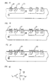
- FIG. 9 schematically depicts an exemplary electronic device, namely, a GaAs-based MOS-FET.
- Numerals 140-147 refer, respectively, to the GaAs body (exemplarily p-type), the source region (exemplarily n-type), the drain region (exemplarily n-type), the drain contact, the source contact, the Ga 2 O 3 gate oxide, the gate contact and the field oxide (optionally also Ga 2 O 3 ).
- Associated with the interface between 140 and 145 is an interface state density ⁇ 10 11 /cm 2 .eV, and typically a recombination velocity ⁇ 10 4 cm/s.
- FIG. 10 schematically depicts another exemplary electronic device, namely, a GaAs-based HBT.
- Numerals 150-158 refer, respectively, to the collector contact, the GaAs substrate (typically n + ), the GaAs collector layer (typically n - ), the GaAs base layer (typically p + ), the emitter layer (exemplarily n-type graded AlGaAs), the emitter contact layer (exemplarily n + AlGaAs), the base contact, the emitter contact and the Ga 2 O 3 passivation layer.
- the above specified characteristics Associated with the interface between the semiconductor material and oxide layer 158 are the above specified characteristics.
- FIG. 11 schematically depicts an exemplary opto-electronic device, namely, a GaAs-based solar cell with Ga 2 O 3 antireflection coating.
- Numerals 160-166 refer, respectively, to the substrate (e.g., GaAs), an n-GaAs layer, a p-GaAs layer, a p + -AlGaAs layer, a p + GaAs contact layer, a metallization layer, and Ga 2 O 3 AR layer.
- the interface between 163 and 166 has the above specified characteristics.
- devices according to the invention are structurally similar or identical to the corresponding (existing or proposed) prior art structures.
- these devices will have substantially improved characteristics.
- the presence of the improved Ga 2 O 3 passivation layer will result in significantly reduced recombination in the extrinsic base region, with attendant improvement in device characteristics.
- GaAs/Ga 2 O 3 structures according to the invention that comprise a dielectric layer deposited as described above (i.e., using a Gd 3 Ga 5 O 12 source) has revealed the presence of a significant amount of Gd in the dielectric layer.
- the Gd concentration is typically highest at or near the surface of the dielectric layer, but is substantially (e.g., by up to three orders of magnitude) less close to the semiconductor/dielectric interface. Due to experimental limitations the dielectric composition directly at the interface has not been determined, but is expected to be essentially pure Ga 2 O 3 , with at most about 100 ppm of Gd.
- FIG. 12 shows in flow chart form a MOS-FET manufacturing process
- FIGs. 13-17 schematically depict various steps of device processing.
- Steps A and B of FIG. 12 respectively require provision of a GaAs substrate and formation of a patterned implant mask.
- the substrate typically is a conventional semi-insulating GaAs wafer, but could be such a wafer with one or more epitaxial layers thereon.
- the discussion below will be in terms of a conventional (100) semi-insulating GaAs substrate.
- Formation of a patterned implant mask exemplarily involves deposition of a thin layer of dielectric material (e.g., SiO 2 , SiN x , SiO x N y , exemplarily 40-200 nm thick) on the major surface of the substrate, deposition of a conventional photoresist layer on the dielectric layer, and patterning of the photoresist layer such that appropriate windows are formed through the photoresist of the dielectric. This is followed by ion implantation (see step C) into the GaAs material that underlies the windows. Steps B and C will typically be repeated one or more times, to attain the dopant distribution shown in FIG. 13. Provision of the dielectric layer is optional but preferred.
- dielectric material e.g., SiO 2 , SiN x , SiO x N y , exemplarily 40-200 nm thick
- FIG. 13 shows semi-insulating GaAs substrate 181 and dielectric layer 182. Implanted regions are shown, the implants selected to facilitate formation of a p- MOS-FET 180 and a n-MOS-FET 188. Only the steps leading to formation of the p-MOS-FET will be discussed in detail, since those leading to the n-MOS-FET are either identical or are obvious variations, e.g., substitution of a p-implant for an n-implant.
- n-type region 183 is formed by implantation of Si or S through dielectric layer 182 in photoresist-defined areas of the wafer. After removal of the photoresist mask, a new mask for implantation of additional Si or S into channel contact 184 is provided, and the n + channel contact is formed. This is followed by formation (by Be or Zn implantation) of p + source 185 and p + drain 186. This in turn is optionally followed by formation (by ion implantation) of p source and drain regions 187 and 189, respectively.
- Step D of FIG. 12 involves annealing of the ion implanted substrate under conditions effective for activating the implanted ions, with or without dielectric layer 182 on the substrate.
- the implant activation anneal exemplarily is accomplished in rapid thermal anneal (RTA) apparatus, typically at a temperature in the range 780-860°C for a time in the range 2-5 minutes.
- RTA rapid thermal anneal
- the dielectric layer is removed (e.g., with HF), and the wafer is heated in an evacuable reactor to a temperature in the above range, with the wafer in contact with an As-containing atmosphere.
- the wafer when the wafer reached 300°C, the wafer was maintained at that temperature for 5 minutes under flowing H 2 , followed by heating to 825°C under H 2 and AsH 3 (H 2 : AsH 3 flow 70:1). The wafer was maintained at 825°C for 5 minutes, followed by cooling to room temperature.
- H 2 + arsine elemental arsenic vapor could be used.
- the atmosphere contains enough As or As-containing species (e.g., arsine) to prevent net loss of As from the substrate surface.
- the required partial pressure of As or As-containing species depends inter alia on the annealing temperature, and thus cannot be specificed in generality. However, a minor amount of experimentation will typically suffice to determine appropriate conditions.
- Step E of FIG. 12 typically involves formation of a dielectric layer (exemplarily about 200 nm of SiO 2 ) on the wafer surface, followed by formation of an appropriately patterned photoresist layer that has windows for channel contact, source contact and drain content. In the window regions, the dielectric material is removed by conventional etch, e.g., with HF.
- numeral 191 refers to the dielectric layer, and 192 to the photoresist.
- Step E of FIG. 12 further comprises deposition of ohmic contacts.
- p-contact metal exemplarily 25 nm AuBe/200 nm Au
- a new photoresist layer is deposited and patterned for n-contact metallization, using, for instance, (5 nm Ni/5 nm Ge/10 nm AuGe/20 nm Mo/200 nm Au).
- FIG. 20 shows the result of the metallization, wherein numeral 201 refers to the n-contact metal of the channel contact, and numerals 202 and 203 refer to the p-contact metal of the source and drain contact, respectively.
- Ohmic contact deposition prior to gate oxide formation is not a requirement, and the deposition could be performed subsequent to gate oxide formation.
- Step F of FIG. 12 involves removal of native oxides (and possibly other contaminants) from the wafer surface.
- the removal has to be carried out such that an essentially atomically clean, essentially atomically ordered, surface results.
- Creation of such a "reconstructed" surface is an important aspect of the process according to the invention. It can be accomplished in any appropriate manner, and will typically be carried out under high vacuum (e.g., pressure ⁇ 10 -8 Torr).
- high vacuum e.g., pressure ⁇ 10 -8 Torr.
- thermal desorption e.g., 5 minutes at 580°C, As overpressure at 10 -6 Torr to protect the wafer surface
- low damage dry etching techniques such as ECR with H 2 plasma or atomic hydrogen.
- the gate oxide layer is formed (step G of FIG. 12) in situ on the reconstructed surface, i.e., without removal of the wafer from the high vacuum, exemplarily as described in the above cited paper by Hong et al. Not only is the oxide layer grown in situ, but the time between completion of surface reconstruction and commencement of oxide deposition is desirably kept to a minimum, in order to avoid significant (e.g., in excess of 100 Langmuirs) contamination of the surface.
- the oxide layer thickness will typically be in the approximate range 5-150 nm, and the layer will have overall composition Ga x A y O z where x ⁇ o, and the other symbols are as defined below.
- the wafer is maintained at a temperature of at most 580°C under arsenic overpressure (e.g., 10 -6 Torr As) during gate oxide deposition.
- arsenic overpressure e.g. 10 -6 Torr As
- the oxide typically is deposited substantially uniformly over the whole wafer surface, but deposition could, at least in principle, be limited to particular portions of the surface, these portions including the gate region between source and drain of at least one MOS-FET.
- the oxide is patterned to expose the previously formed channel, source and drain contacts of the MOS-FETs, as indicated by step H of FIG. 12.
- the patterning can be done using conventional photolithography and etching, e.g., in HCI solution.
- FIG. 16 schematically shows two devices after gate oxide patterning, with numeral 211 referring to the patterned gate oxide.
- Patterning of the gate oxide layer is followed by gate metallization, also per step H of FIG. 12.
- This can be conventional, involving for instance e-beam deposition of 25 mm Ti/50 nm Pt/300 nm Au, and lift-off.
- this step can also include formation of interconnections, including providing connections (not shown in FIG. 17) to channel, source, drain and gate contacts of the various MOS-FETs.
- numerals 221 and 222 refer to the gate contact of the p-MOS-FET and n-MOS-FET, respectively.
- Step I of FIG. 12 refers to a variety of, typically conventional, steps that will typically be required to complete an IC according to the invention, e.g., testing, dicing of the wafer into chips, wire bonding, encapsulation, etc.
- MOS-FET desirably will be electrically connected in conventional manner to other electronic devices, including other MOS-FETs, to form an integrated circuit.
- the complementary MOS-FETs of FIG. 17 can be connected as shown in FIG. 18 to provide an inverter.
- numeral 231 refers to a n-channel enhancement mode GaAs MOS-FET substantially as shown in FIG. 17
- 232 refers to a p-channel enhancement mode GaAs MOS-FET, also substantially as shown in FIG. 17.
- the circuit per se is conventional, but the implementation in GaAs MOS-FET technology is novel, to the best of our knowledge.
- the combination of FIG. 18 is representative of circuits according to the invention.
- the above described process not only is suitable for producing GaAs-based planar n-channel and p-channel MOS-FETs on the same substrate, but can also be used to combine such MOS-FETs with GaAs (metal-semiconductor) MES-FETs.
- the gate oxide exemplarily is removed from the respective gate region, and an appropriate metal (e.g., Ti/Pt/Au) is deposited in the gate region to provide a Schottky barrier contact.
- GaAs-based MES-FETs are known and do not require detailed description.
- GaAs MES-FETs with GaAs MOS-FETs (including complementary enhancement type GaAs-MOSFETs) does, to the best of our knowledge, not exist in the prior art. Availability of this ability is expected to provide circuit designers with greater design freedom, and to lead to manufacture of a wide range of GaAs-based digital (but not excluding analog) ICs.
- GaAs MOS-FETs Some differences between prior art GaAs MOS-FETs and GaAs MOS-FETs according to the above description may bear further recitation.
- the source and drain regions are connected by a channel of the same conductivity type as the regions. See, for instance, the above cited paper by Colquhoun et al. Such devices do not exhibit inversion in the channel.
- Some devices require selective etching of the surface of the GaAs wafer, typically to form a notch in the surface to thereby reduce the channel width. See, for instance, the above cited paper by T. Mimura et al., FIGs. 7 and 8, and the Colquhoun et al. paper. No such etching is required for GaAs MOS-FETs according to the invention.
- ohmic contacts can be formed after gate oxide deposition.
- a cap layer e.g., a SiO 2 layer
- the method is carried out such that the device is, after gate oxide formation, not subjected to a temperature above about 300°C in air, or ⁇ 700°C in UHV.
- a highly preferred feature is implant activation anneal in an As-containing atmosphere, with the partial pressure of As or As-containing species selected to prevent net loss of As from the surface.
- MOS-FETs produced according to the invention have been tested in conventional fashion, and have been found to have excellent characteristics.
- a p-MOS-FET was fabricated as follows.
- a conventional semiinsulating (100) oriented GaAs wafer (sheet resistivity about 10 8 ⁇ cm) was provided.
- a 50 nm layer of SiO 2 was deposited, by conventional PECVD, a 50 nm layer of SiO 2 .
- a 2.2 ⁇ m layer of conventional photoresist (AZ 1818) was formed on the SiO 2 layer and patterned to form an ion implantation mask, with a window through the mask that defined the n channel for the p-MOS-FET.
- Si ions were then implanted through the window (150 keV, 5 x 10 13 cm -2 ).
- Implant conditions were, respectively, as follows: 75 KeV, 6 x 10 13 cm -2 , Si; 30 KeV, 7 x 10 -3 cm -2 , Be; and 25 KeV, 3 x 10 12 cm -2 , Be.
- the resist and SiO 2 were removed with acetone and HF (1:1HF:H 2 O), respectively.
- Implant activation was carried out in the reactor of a MOCVD system. The temperature of the wafer was raised, with H 2 admitted into the reactor when the wafer temperature had reached 300°C. The wafer was maintained under these conditions for 5 minutes, followed by admission of arsine and gradual raising of the temperature to 825°C, and maintenance of the wafer under these conditions for 5 minutes.
- the arsine: H 2 flow ratio and system pressure were 1:70 and 45 Torr, respectively.
- the wafer was allowed to cool to 450°C under arsine/H 2, and then to room temperature under H 2 , and transferred to a MBE system for surface reconstruction and gate oxide deposition.
- the wafer was mounted on a Mo block with indium and heated to 580°C for 5 minutes to desorb surface contaminants such as native oxides.
- the background pressure in the reactor of the MBE system was 10 -10 Torr, and an arsenic pressure of 10 -6 Torr was maintained in the reactor to protect the wafer surface.
- RHEED was used to monitor the sample surface. The above described treatment resulted in an essentially atomically clean, atomically ordered wafer surface.
- the wafer Upon completion of surface reconstruction, the wafer was transferred under UHV (10 -10 Torr) to a second chamber of the MBE system. A 40 nm layer of oxide was deposited over the wafer surface at a rate of about 0.02 nm/sec, substantially as described in the above cited paper by Hong et al. Briefly, the wafer was at 550°C, the background pressure in the chamber was less than 10 -9 Torr, and the oxide was formed by e-beam evaporation.
- UHV 10 -10 Torr
- the ohmic contacts were defined.
- a conventional photoresist layer (AZ 1818) was applied and patterned in conventional manner such that the gate source and drain contact regions were exposed.
- the gate oxide was then removed from the exposed regions with 1:1 HCl:H 2 O, and contact metal (25 nm AuBe/200 nm Au) was deposited by means of an e-beam deposition system.
- a conventional acetone life-off technique was used to remove the undesired metallization.
- a 1.2 ⁇ m resist layer (AZ 1811) was applied and patterned, and used to define gate and final metal contacts at the same time.
- a Ti/Pt/Au layer (25 nm/50 nm/300 nm, respectively) was deposited by means of an e-beam deposition system. Unwanted metallization was removed with a conventional acetone lift-off technique, leaving channel, source, drain and gate contacts.
- the thus produced device (40 x 50 ⁇ m 2 gate geometry) was tested, and found to have the following characteristics:
- FIG. 20 shows the drain I-V characteristics of the exemplary MOS-FET
- FIG. 21 shows drain current vs. gate voltage.
- a pair of complementary MOS-FETs on a common substrate was produced substantially as described above, except that the ion implantation is modified to produce implanted regions substantially as shown in FIG. 18.
- the pair of MOS-FETs is connected as shown in FIG. 18 to form an inverter circuit. The circuit is tested and performs as expected.
- a multiplicity of n-MOS-FETs, p-MOS-FETs and n- and p-MES-FETs are formed on a common substrate, substantially as described in Example 2, except that the gate oxide is removed from some of the n-type devices and some of the p-type devices, and 25 nm Ti/30 nm Pt/300 nm Au is deposited in the gate regions of these devices. After provision of conductive interconnects between the devices, the resulting circuit is tested and performs as expected.
- the presence of the Gd is undesirable, and that ideally the film should be pure Ga oxide. See, for instance, US patent 5,597,768, which discloses at col. 1, lines 39-45 that"...
- the major problem is that some of the Gd 2 O 3 (about 0.1% according to the patent) is incorporated into the thin film as impurities creating defects increasing the bulk trap density.
- the '768 patent teaches use of different evaporation source materials that "contain” Ga 2 O 3 and another oxide having a melting temperature that is more than 700°C above the sublimation temperature of Ga 2 O 3 .
- One such material is MgGa 2 O 4 , which is said to "contain” MgO and Ga 2 O 3 .
- MgGa 2 O 4 instead of GGG is said to result in”... drastically reduced incorporation of the undesired specie in the oxide film and in significantly lower bulk trap density in the oxide film.” See col. 3, lines 18-21 of the '768 patent.
- the '768 patent does not provide any experimental data
- the oxide thin film desirably contains a substantial amount of Gd (or other appropriate metal element), Indeed, we have found that a film that is formed by evaporation from pure Ga 2 O 3 powder (and thus is essentially pure Ga oxide) is generally not of device quality, whereas a film that is formed by evaporation from pure Gd 2 O 3 (and thus is essentially pure Gd oxide) is generally of device quality, with low interface state density.
- FIG. 22 shows data on the I-V (current-voltage) characteristics of very thin oxide layers on GaAs, with a conventional metal contact defining the aera of the MOS capacitor. As can be readily seen from FIG.
- a 40 nm thick Ga 2 O 3 film has essentially zero breakdown voltage for negative bias, with relatively high leakage for positive bias, and thus is unsuitable for most device applications, whereas a 18.5 nm thick Gd 2 O 3 film conducts a mere 10 -8 A/cm 2 at + or -3V.
- Films of intermediate composition show intermediate breakdown voltages.
- a thin oxide film that is formed by in situ co-evaporation from two separate sources generally will be of device quality, provided the evaporation rates are selected such that the content of Gd (or other appropriate metal element) is at least about 10 atomic % of the total metal content, preferably at least 20 atomic %.
- GaAs substrates were prepared as described above (resulting in an essentially atomically clean and atomically ordered surface), with the evaporations carried out in situ, without exposure of the samples to the atmosphere.
- Ga can exist in the 1+, 2+ and 3+ oxidation states, and that there are electro-positive elements (to be termed "stabilizers") that can stabilize Ga in the 3+ state.
- the stabilizers for Ga is Gd, having Pauling electronegativity 1.1.
- the stabilizers for Ga are Sc, Y, the other rare earths, the alkaline earths and the alkalis.
- the oxide film is formed by deposition from 2 (or more) separate deposition sources (e.g., e-beam evaporation sources), with the deposition parameters selected such that the resulting film has overall composition Ga x A y O z , where A is one or more electropositive stabilizer element for stabilizing Ga in the 3+ oxidation state, and x > 0.
- y/(x+y) is greater than or equal to 0.1, preferably ⁇ 0.2, and z is selected to satisfy the requirement that both Ga and A are substantially fully oxidized.
- the oxide film is formed by deposition of A-oxide, without deposition of Ga-oxide.
- the film thus has overall composition AO z , with z selected such that A is substantially fully oxidized.
- A is selected from the group consisting of Sc, Y, the rare earth metals (atomic number 57.71), the alkaline earths (e.g., Be, Mg, Ca, Sr, Ba), and the alkalis (e.g., Li, Na, K, Rb, Cs).
- the alkali elements generally are not preferred, due to their relative instability to moisture and incompatibility with semiconductor device processing conditions.
- the currently preferred stabilizer elements are Sc, Y the rare earths (atomic number 57-71) and the alkaline earths, with Sc, Y, La, Nd, Gd, Dy, Ho, Er and Lu being currently most preferred.
- Ga (and A) are substantially fully oxidized does not mean that 100% of all Ga ions have to be in the 3+ ionization state. Typically acceptable results are obtained if 80% or more of all Ga is in the 3+ state, with 80% or more of A also being fully oxidized.
- a mixed oxide of composition Ga x A y O z is not necessarily a homogeneous material of that composition.
- the material contains microscopic regions of Ga-oxide as well as microscopic regions of A-oxide.
- FIG. 23 shows C-V (capacitance-voltage) data for a 19 nm thick film of Gd 2 O 3 on n-type (2 x 10 18 cm -3 ) GaAs of (100) orientation.
- the aera of the MOS capacitor was 4.4 x 10 -5 cm 2 .
- FIG. 23 clearly shows accumulation and inversion at low frequency. The data establishes the suitability of the oxide film for device applications, including for MOS-FETs.
- FIG. 24 shows similar data for a 32 nm thick Ga- and Gd-containing mixed oxide film, with about 22% of the total metal content being Gd.
- the data also shows accumulation and inversion, substantially as the data of FIG. 23.
- the article comprises a planar enhancement mode MOS-FET with inversion channel.
- a MOS-FET is fabricated substantially as disclosed in Example 1, except that a Gd- and Ga-containing oxide film is deposited by simultaneous e-beam evaporation from a source containing Ga 2 O 3 powder and a source containing Gd 2 O 3 powder, with the evaporation rates selected to yield a film having Gd - 22% of the total metal content.
- the MOS-FET performs substantially as the device of Example 1.
- a MOS-FET is fabricated substantially as in Example 4, except that the oxide film is Gd 2 O 3 .
- the MOS-FET performs substantially as the device of Example 4.
Applications Claiming Priority (2)
| Application Number | Priority Date | Filing Date | Title |
|---|---|---|---|
| US93557 | 1998-06-08 | ||
| US09/093,557 US5962883A (en) | 1994-03-23 | 1998-06-08 | Article comprising an oxide layer on a GaAs-based semiconductor body |
Publications (2)
| Publication Number | Publication Date |
|---|---|
| EP0964453A2 true EP0964453A2 (de) | 1999-12-15 |
| EP0964453A3 EP0964453A3 (de) | 2000-05-10 |
Family
ID=22239593
Family Applications (1)
| Application Number | Title | Priority Date | Filing Date |
|---|---|---|---|
| EP99304032A Withdrawn EP0964453A3 (de) | 1998-06-08 | 1999-05-25 | Vorrichtung mit einer Oxidschicht auf GaAs-basierendem Halbleiterkörper und Verfahren zur Herstellung |
Country Status (4)
| Country | Link |
|---|---|
| US (1) | US5962883A (de) |
| EP (1) | EP0964453A3 (de) |
| JP (1) | JP2000068510A (de) |
| KR (1) | KR20000006005A (de) |
Cited By (1)
| Publication number | Priority date | Publication date | Assignee | Title |
|---|---|---|---|---|
| WO2002009157A2 (en) * | 2000-07-21 | 2002-01-31 | Motorola, Inc. | Alkali earth metal oxide gate insulators |
Families Citing this family (31)
| Publication number | Priority date | Publication date | Assignee | Title |
|---|---|---|---|---|
| US6469357B1 (en) * | 1994-03-23 | 2002-10-22 | Agere Systems Guardian Corp. | Article comprising an oxide layer on a GaAs or GaN-based semiconductor body |
| US6376337B1 (en) * | 1997-11-10 | 2002-04-23 | Nanodynamics, Inc. | Epitaxial SiOx barrier/insulation layer |
| US6693033B2 (en) | 2000-02-10 | 2004-02-17 | Motorola, Inc. | Method of removing an amorphous oxide from a monocrystalline surface |
| US6936900B1 (en) * | 2000-05-04 | 2005-08-30 | Osemi, Inc. | Integrated transistor devices |
| US6555946B1 (en) | 2000-07-24 | 2003-04-29 | Motorola, Inc. | Acoustic wave device and process for forming the same |
| AU2001288239A1 (en) * | 2000-08-10 | 2002-02-25 | Walter David Braddock Iv | Integrated transistor devices |
| US6638838B1 (en) | 2000-10-02 | 2003-10-28 | Motorola, Inc. | Semiconductor structure including a partially annealed layer and method of forming the same |
| FR2820241B1 (fr) * | 2001-01-31 | 2003-09-19 | Saint Gobain | Substrat transparent muni d'une electrode |
| US6673646B2 (en) | 2001-02-28 | 2004-01-06 | Motorola, Inc. | Growth of compound semiconductor structures on patterned oxide films and process for fabricating same |
| US6709989B2 (en) | 2001-06-21 | 2004-03-23 | Motorola, Inc. | Method for fabricating a semiconductor structure including a metal oxide interface with silicon |
| US6531740B2 (en) | 2001-07-17 | 2003-03-11 | Motorola, Inc. | Integrated impedance matching and stability network |
| US6646293B2 (en) | 2001-07-18 | 2003-11-11 | Motorola, Inc. | Structure for fabricating high electron mobility transistors utilizing the formation of complaint substrates |
| US6693298B2 (en) | 2001-07-20 | 2004-02-17 | Motorola, Inc. | Structure and method for fabricating epitaxial semiconductor on insulator (SOI) structures and devices utilizing the formation of a compliant substrate for materials used to form same |
| US6594414B2 (en) | 2001-07-25 | 2003-07-15 | Motorola, Inc. | Structure and method of fabrication for an optical switch |
| US6667196B2 (en) | 2001-07-25 | 2003-12-23 | Motorola, Inc. | Method for real-time monitoring and controlling perovskite oxide film growth and semiconductor structure formed using the method |
| US6585424B2 (en) | 2001-07-25 | 2003-07-01 | Motorola, Inc. | Structure and method for fabricating an electro-rheological lens |
| US6589856B2 (en) | 2001-08-06 | 2003-07-08 | Motorola, Inc. | Method and apparatus for controlling anti-phase domains in semiconductor structures and devices |
| US6639249B2 (en) | 2001-08-06 | 2003-10-28 | Motorola, Inc. | Structure and method for fabrication for a solid-state lighting device |
| US6673667B2 (en) | 2001-08-15 | 2004-01-06 | Motorola, Inc. | Method for manufacturing a substantially integral monolithic apparatus including a plurality of semiconductor materials |
| US6756320B2 (en) * | 2002-01-18 | 2004-06-29 | Freescale Semiconductor, Inc. | Method of forming article comprising an oxide layer on a GaAs-based semiconductor structure |
| US7442654B2 (en) * | 2002-01-18 | 2008-10-28 | Freescale Semiconductor, Inc. | Method of forming an oxide layer on a compound semiconductor structure |
| US6933244B2 (en) * | 2002-01-22 | 2005-08-23 | Massachusetts Institute Of Technology | Method of fabrication for III-V semiconductor surface passivation |
| US6833556B2 (en) | 2002-08-12 | 2004-12-21 | Acorn Technologies, Inc. | Insulated gate field effect transistor having passivated schottky barriers to the channel |
| US7084423B2 (en) | 2002-08-12 | 2006-08-01 | Acorn Technologies, Inc. | Method for depinning the Fermi level of a semiconductor at an electrical junction and devices incorporating such junctions |
| US6770536B2 (en) * | 2002-10-03 | 2004-08-03 | Agere Systems Inc. | Process for semiconductor device fabrication in which a insulating layer is formed on a semiconductor substrate |
| US7662698B2 (en) * | 2006-11-07 | 2010-02-16 | Raytheon Company | Transistor having field plate |
| WO2013077954A1 (en) | 2011-11-23 | 2013-05-30 | Acorn Technologies, Inc. | Improving metal contacts to group iv semiconductors by inserting interfacial atomic monolayers |
| US9620611B1 (en) | 2016-06-17 | 2017-04-11 | Acorn Technology, Inc. | MIS contact structure with metal oxide conductor |
| US10170627B2 (en) | 2016-11-18 | 2019-01-01 | Acorn Technologies, Inc. | Nanowire transistor with source and drain induced by electrical contacts with negative schottky barrier height |
| JP6995307B2 (ja) * | 2017-08-04 | 2022-01-14 | 出光興産株式会社 | 半導体装置及び半導体装置の製造方法 |
| KR102446402B1 (ko) * | 2017-10-12 | 2022-09-21 | 어플라이드 머티어리얼스, 인코포레이티드 | 플라즈마 유발 손상을 감소시키기 위한 프로세스 |
Citations (3)
| Publication number | Priority date | Publication date | Assignee | Title |
|---|---|---|---|---|
| US3663870A (en) * | 1968-11-13 | 1972-05-16 | Tokyo Shibaura Electric Co | Semiconductor device passivated with rare earth oxide layer |
| EP0203578A2 (de) * | 1985-05-30 | 1986-12-03 | Hitachi, Ltd. | Halbleiteranordnung mit epitaxialer isolierender Schicht und Verfahren zu deren Herstellung |
| EP0863552A1 (de) * | 1997-02-24 | 1998-09-09 | Lucent Technologies Inc. | GaAs-basierender MOSFET und Verfahren zur Herstellung |
Family Cites Families (6)
| Publication number | Priority date | Publication date | Assignee | Title |
|---|---|---|---|---|
| US4749255A (en) * | 1985-12-09 | 1988-06-07 | American Telephone And Telegraph Company, At&T Bell Laboratories | Coating for optical devices |
| US4859253A (en) * | 1988-07-20 | 1989-08-22 | International Business Machines Corporation | Method for passivating a compound semiconductor surface and device having improved semiconductor-insulator interface |
| US5055445A (en) * | 1989-09-25 | 1991-10-08 | Litton Systems, Inc. | Method of forming oxidic high Tc superconducting materials on substantially lattice matched monocrystalline substrates utilizing liquid phase epitaxy |
| US5550089A (en) * | 1994-03-23 | 1996-08-27 | Lucent Technologies Inc. | Gallium oxide coatings for optoelectronic devices using electron beam evaporation of a high purity single crystal Gd3 Ga5 O12 source. |
| US5451548A (en) * | 1994-03-23 | 1995-09-19 | At&T Corp. | Electron beam deposition of gallium oxide thin films using a single high purity crystal source |
| US5597768A (en) * | 1996-03-21 | 1997-01-28 | Motorola, Inc. | Method of forming a Ga2 O3 dielectric layer |
-
1998
- 1998-06-08 US US09/093,557 patent/US5962883A/en not_active Expired - Lifetime
-
1999
- 1999-05-25 EP EP99304032A patent/EP0964453A3/de not_active Withdrawn
- 1999-06-08 KR KR1019990021102A patent/KR20000006005A/ko not_active Application Discontinuation
- 1999-06-08 JP JP11160428A patent/JP2000068510A/ja active Pending
Patent Citations (3)
| Publication number | Priority date | Publication date | Assignee | Title |
|---|---|---|---|---|
| US3663870A (en) * | 1968-11-13 | 1972-05-16 | Tokyo Shibaura Electric Co | Semiconductor device passivated with rare earth oxide layer |
| EP0203578A2 (de) * | 1985-05-30 | 1986-12-03 | Hitachi, Ltd. | Halbleiteranordnung mit epitaxialer isolierender Schicht und Verfahren zu deren Herstellung |
| EP0863552A1 (de) * | 1997-02-24 | 1998-09-09 | Lucent Technologies Inc. | GaAs-basierender MOSFET und Verfahren zur Herstellung |
Non-Patent Citations (3)
| Title |
|---|
| HONG M ET AL: "Growth of Ga2O3(Gd2O3) using molecular beam epitaxy technique-key to first demonstration of GaAs MOSFETs" COMPOUND SEMICONDUCTORS 1997. PROC. TWENTY-FOURTH INTERNATIONAL SYMPOSIUM ON COMPOUND SEMICONDUCTORS, SAN DIEGO, CA, USA, 8 - 11 September 1997, pages 319-324, XP002132669 IEEE, New York, NY, USA; ISBN: 0-7503-0556-8 * |
| HONG M ET AL: "Novel Ga2O3(Gd2O3) passivation techniques to produce low Dit oxide-GaAs interfaces" PROC. NINTH INTERNATIONAL CONFERENCE ON MOLECULAR BEAM EPITAXY, MALIBU, CA, USA, 5-9 AUG. 1996, vol. 175-176, pt.1, May 1997 (1997-05), pages 422-427, XP004091330 Journal of Crystal Growth, Netherlands ISSN: 0022-0248 * |
| KWO J ET AL: "The (Ga2O3)1-x(Gd2O3)x oxides with x=0-1.0 for GaAs passivation" PROC. 1999 MRS SPRING MEETING - SYMPOSIUM Z, 'COMPOUND SEMICONDUCTOR SURFACE PASSIVATION AND NOVEL DEVICE PROCESSING', SAN FRANCISCO, CA, USA, vol. 573, 5 - 7 April 1999, pages 57-67, XP000889683 Mater. Res. Soc. Symp. Proc., Materials Research Society, Warrendale, PA, USA * |
Cited By (2)
| Publication number | Priority date | Publication date | Assignee | Title |
|---|---|---|---|---|
| WO2002009157A2 (en) * | 2000-07-21 | 2002-01-31 | Motorola, Inc. | Alkali earth metal oxide gate insulators |
| WO2002009157A3 (en) * | 2000-07-21 | 2002-06-20 | Motorola Inc | Alkali earth metal oxide gate insulators |
Also Published As
| Publication number | Publication date |
|---|---|
| US5962883A (en) | 1999-10-05 |
| JP2000068510A (ja) | 2000-03-03 |
| KR20000006005A (ko) | 2000-01-25 |
| EP0964453A3 (de) | 2000-05-10 |
Similar Documents
| Publication | Publication Date | Title |
|---|---|---|
| US5962883A (en) | Article comprising an oxide layer on a GaAs-based semiconductor body | |
| Pearton et al. | Gallium nitride processing for electronics, sensors and spintronics | |
| US5920105A (en) | Compound semiconductor field effect transistor having an amorphous gas gate insulation layer | |
| EP0561567A2 (de) | Legierungen die Gallium und Aluminium enthalten, für Halbleiterkontakte | |
| Arulkumaran et al. | Effects of annealing on Ti, Pd, and Ni/n-Al/sub 0.11/Ga/sub 0.89/N Schottky diodes | |
| JP2000150503A (ja) | GaAsやGaNに基づく半導体基体上に酸化物層を含む物品 | |
| Ohmi | ULSI reliability through ultraclean processing | |
| US6030453A (en) | III-V epitaxial wafer production | |
| US4610731A (en) | Shallow impurity neutralization | |
| KR100516252B1 (ko) | 반도체소자를가진물품및그제조방법 | |
| US5903037A (en) | GaAs-based MOSFET, and method of making same | |
| US6271069B1 (en) | Method of making an article comprising an oxide layer on a GaAs-based semiconductor body | |
| EP0208851A1 (de) | Herstellung eines Halbleiterbauelementes mittels Molekularstrahlepitaxie | |
| US6451711B1 (en) | Epitaxial wafer apparatus | |
| TW509981B (en) | MOCVD-grown Emode HIGFET buffer | |
| Zeindl et al. | Delta‐Doped MESFET with MBE‐Grown Si | |
| EP0987746B1 (de) | Methode zur Herstellung einer integrierten Schaltung mit einer Oxidschicht auf einem GaAs Halbleitersubstrat | |
| JP3126890B2 (ja) | Mis構造を有する半導体装置及びその製造方法 | |
| Sobolev et al. | Capacitance Spectroscopy of Heteroepitaxial AlGaAs/GaAs p–i–n Structures | |
| Merkel et al. | Improved p-channel InAlAsGaAsSb higfet using Ti/Pt/Au ohmic contacts to beryllium implanted GaAsSb | |
| Lee et al. | Au/Ge-based Ohmic contact to an AlGaAs/InGaAs pseudomorphic high electron mobility transistor with an undoped cap layer | |
| Takanashi | Characterization of traps in GaAs/W Schottky diodes by optical and electrical deep‐level transient spectroscopy methods | |
| Ohmi | Technology for High-Power Devices | |
| Imaizumi et al. | Undoped semi‐insulating GaAs epitaxial layers and their characterization | |
| Hong et al. | Growth of Ga/sub 2/O/sub 3/(Gd/sub 2/O/sub 3/) using molecular beam epitaxy technique-key to first demonstration of GaAs MOSFETs |
Legal Events
| Date | Code | Title | Description |
|---|---|---|---|
| PUAI | Public reference made under article 153(3) epc to a published international application that has entered the european phase |
Free format text: ORIGINAL CODE: 0009012 |
|
| 17P | Request for examination filed |
Effective date: 19990604 |
|
| AK | Designated contracting states |
Kind code of ref document: A2 Designated state(s): DE FR GB |
|
| AX | Request for extension of the european patent |
Free format text: AL;LT;LV;MK;RO;SI |
|
| PUAL | Search report despatched |
Free format text: ORIGINAL CODE: 0009013 |
|
| AK | Designated contracting states |
Kind code of ref document: A3 Designated state(s): AT BE CH CY DE DK ES FI FR GB GR IE IT LI LU MC NL PT SE |
|
| AX | Request for extension of the european patent |
Free format text: AL;LT;LV;MK;RO;SI |
|
| AKX | Designation fees paid |
Free format text: DE FR GB |
|
| STAA | Information on the status of an ep patent application or granted ep patent |
Free format text: STATUS: THE APPLICATION IS DEEMED TO BE WITHDRAWN |
|
| 18D | Application deemed to be withdrawn |
Effective date: 20041201 |