EP0962863A2 - Gleichzeitige DASD Wartung für ein auf PCI-Bus gestütztes DASD Subsystem - Google Patents
Gleichzeitige DASD Wartung für ein auf PCI-Bus gestütztes DASD Subsystem Download PDFInfo
- Publication number
- EP0962863A2 EP0962863A2 EP99304027A EP99304027A EP0962863A2 EP 0962863 A2 EP0962863 A2 EP 0962863A2 EP 99304027 A EP99304027 A EP 99304027A EP 99304027 A EP99304027 A EP 99304027A EP 0962863 A2 EP0962863 A2 EP 0962863A2
- Authority
- EP
- European Patent Office
- Prior art keywords
- bus
- input
- bridge circuit
- concurrent maintenance
- coupled
- Prior art date
- Legal status (The legal status is an assumption and is not a legal conclusion. Google has not performed a legal analysis and makes no representation as to the accuracy of the status listed.)
- Withdrawn
Links
- 238000012423 maintenance Methods 0.000 title claims abstract description 75
- 238000004891 communication Methods 0.000 claims abstract description 51
- 230000002093 peripheral effect Effects 0.000 claims abstract description 24
- 238000000034 method Methods 0.000 claims description 26
- 230000004044 response Effects 0.000 claims description 17
- 230000011664 signaling Effects 0.000 claims description 9
- 230000007246 mechanism Effects 0.000 claims description 4
- TXCGAZHTZHNUAI-UHFFFAOYSA-N clofibric acid Chemical compound OC(=O)C(C)(C)OC1=CC=C(Cl)C=C1 TXCGAZHTZHNUAI-UHFFFAOYSA-N 0.000 abstract 1
- 230000001419 dependent effect Effects 0.000 abstract 1
- 238000011144 upstream manufacturing Methods 0.000 description 4
- 230000000694 effects Effects 0.000 description 3
- 238000010586 diagram Methods 0.000 description 2
- 238000003780 insertion Methods 0.000 description 2
- 230000037431 insertion Effects 0.000 description 2
- 238000012986 modification Methods 0.000 description 2
- 230000004048 modification Effects 0.000 description 2
- 230000009467 reduction Effects 0.000 description 2
- 238000013519 translation Methods 0.000 description 2
- 230000009471 action Effects 0.000 description 1
- 230000006978 adaptation Effects 0.000 description 1
- 238000013459 approach Methods 0.000 description 1
- 238000013461 design Methods 0.000 description 1
- 238000009434 installation Methods 0.000 description 1
- 230000008569 process Effects 0.000 description 1
- 238000011084 recovery Methods 0.000 description 1
Images


Classifications
-
- G—PHYSICS
- G06—COMPUTING; CALCULATING OR COUNTING
- G06F—ELECTRIC DIGITAL DATA PROCESSING
- G06F13/00—Interconnection of, or transfer of information or other signals between, memories, input/output devices or central processing units
- G06F13/38—Information transfer, e.g. on bus
- G06F13/382—Information transfer, e.g. on bus using universal interface adapter
- G06F13/385—Information transfer, e.g. on bus using universal interface adapter for adaptation of a particular data processing system to different peripheral devices
-
- G—PHYSICS
- G06—COMPUTING; CALCULATING OR COUNTING
- G06F—ELECTRIC DIGITAL DATA PROCESSING
- G06F1/00—Details not covered by groups G06F3/00 - G06F13/00 and G06F21/00
- G06F1/26—Power supply means, e.g. regulation thereof
- G06F1/32—Means for saving power
- G06F1/3203—Power management, i.e. event-based initiation of a power-saving mode
-
- G—PHYSICS
- G06—COMPUTING; CALCULATING OR COUNTING
- G06F—ELECTRIC DIGITAL DATA PROCESSING
- G06F11/00—Error detection; Error correction; Monitoring
- G06F11/07—Responding to the occurrence of a fault, e.g. fault tolerance
- G06F11/16—Error detection or correction of the data by redundancy in hardware
- G06F11/20—Error detection or correction of the data by redundancy in hardware using active fault-masking, e.g. by switching out faulty elements or by switching in spare elements
- G06F11/2053—Error detection or correction of the data by redundancy in hardware using active fault-masking, e.g. by switching out faulty elements or by switching in spare elements where persistent mass storage functionality or persistent mass storage control functionality is redundant
- G06F11/2089—Redundant storage control functionality
Definitions
- the present invention relates to the field of computer system maintenance, and in particular, to concurrent maintenance of peripheral component interconnect (PCI) based direct access storage devices (DASDs, i.e., disk drives).
- PCI peripheral component interconnect
- DASDs direct access storage devices
- Typical medium to large size computer systems include at least one backplane, which is essentially a connecting board having integrated wiring and bus slots or other connectors, for interconnecting various computer system circuits designed to connect to the backplane.
- the backplanes are used to connect input-output (I/O) circuits, also commonly referred to as adapters or controller cards, for use in interfacing peripheral devices, for example, direct access storage devices (DASDs, e.g., hard disk drives), to the rest of the computer system.
- I/O circuits are generally disposed on modules or cards which have standard connectors for plug-in to the backplane at bus sockets or slots. This allows for easy maintenance including removal, servicing, upgrading and replacement by service personnel.
- an interface circuit card is used to couple a DASD parallel or serial input/output bus to the computer system bus via the backplane.
- DASD backplanes and DASD towers there may be one or more backplanes and/or enclosures dedicated to DASDs, and these are referred to herein as DASD backplanes and DASD towers, respectively.
- IBM AS/400 IBM AS/400 (IBM and AS/400 are registered trademarks of International Business Machines Corporation).
- An AS/400 computer system for example, in its multi-tower configuration, includes towers interconnected by at least one host system bus, and also interconnected by a control network called the system power control network (SPCN).
- SPCN system power control network
- the known a system power control network (SPCN) is disclosed in U. S. Patent No. 5,117,430, for example.
- the SPCN is a low volume serial network used, for instance, to monitor power conditions at a plurality of interconnected nodes in a multi-tower computer system.
- the SPCN may include one or more microprocessors which are operational to, for example, monitor the status of, and make occasional adjustments to, the power conditions at the respective computer system nodes.
- IPL initial program load
- the SPCN microprocessors gather computer system configuration information ahead of and independently of the computer system main communication paths.
- PCI backplane There are a variety of standard bus types and associated slot connectors currently in use in computer system backplanes, including serial and parallel versions of SCSI (Small Computer System Interconnect), and the currently popular PCI (Peripheral Component Interconnect), for example.
- a backplane includes primarily PCI type (slot) connections, it will be referred to herein as a PCI backplane.
- a PCI backplane has a host PCI bus integrated on the backplane, and includes at least one PCI bridge circuit (PCIB) which couples the local PCI slot connections thereon to the computer system host bus, and to any other local PCI buses/connections present, thereby "bridging" the buses.
- the computer system host bus could also be a PCI bus or another type of bus. It is possible for an SCSI-based I/O controller, which couples to a peripheral device over an SCSI bus, to be disposed on a card configured to plug-in to a PCI slot on a PCI backplane.
- DASDs typically connect directly to either a serial or a parallel SCSI I/O bus.
- One possible DASD system configuration therefore, includes one or more DASDs connected by an SCSI bus to an SCSI DASD I/O card, which is plugged into a PCI slot on a PCI backplane of an AS/400 computer system. This type of DASD configuration will be referred to as a PCI-based DASD configuration or subsystem herein.
- CM concurrent maintenance
- failed or failing DASDs should be replaceable in a concurrent maintenance operation, but to do so requires the SCSI bus to be quiesced while the DASD device is powered down and removed, and a replacement reinstalled and powered on, in order to prevent errors and voltage transients that may affect other devices.
- ANSI's SES identifies the use and connection of an SES microprocessor to the SCSI bus.
- the ANSI-SES specifies that the SCSI bus must download enclosure information and services to an SES processor on the SCSI bus.
- One of the possible uses identified is to issue commands through the SCSI bus (using SCSI Diagnostic Mode Pages) to the SES processor, directing some 10 pins on the processor to turn on/off FETs or regulators on a DASD backplane to power on/off the DASD for concurrent maintenance (CM) activities.
- SCSI bus using SCSI Diagnostic Mode Pages
- SCSI Power Management identifies various SCSI commands that can be used to control various aspects of power consumed by a DASD, and includes the concept of powering the DASD completely on and off.
- the above-mentioned ANSI solutions have some drawbacks and limitations which make them significantly less than optimal solutions. For example, it is possible that the reason for needing a DASD maintenance action may be that the SCSI bus itself is inoperative. Since the above ANSI solutions make use of the SCSI bus for signalling and control, they may not be able to effectively and efficiently handle concurrent maintenance in the situation where the SCSI bus is causing the fault.
- one SES processor is required for each SCSI bus, so that costs disadvantageously increase substantially with each SCSI bus added.
- an electrical system having a system power controller and at least one system component coupled to the electrical system by a first communications path having a input/output controller thereon, a method comprising: enabling concurrent maintenance of the at least one system component by exchanging signals between the input/output controller and the system power controller over a second communications path different from the first communications path, so that the system power controller thereby controls power to the system component subject to concurrent maintenance.
- apparatus for enabling concurrent maintenance of a system component coupled by a first communication path to an electrical system, wherein the first communication path includes a system bus, a local bus and a bus bridge circuit bridging the local bus and the system bus, the apparatus comprising: a system power controller which controls power to the system component; and a second communication path which connects the system power controller and the bus bridge circuit, through which concurrent maintenance signals are communicated.
- a method of enabling concurrent maintenance in a computer system having at least one peripheral device coupled by a first bus to an input-output circuit, the input-output circuit coupled to a computer system host processor through a host bus and a host bus bridge circuit, the computer system further having a system power control network which controls power to each component of the computer system, the system power control network being interfaced to the at least one input/output circuit by a second different bus, the method comprising: signalling to the input/output circuit a request for concurrent maintenance from the computer system through the host bus and host bridge circuit; signalling to the system power control network over the second bus, with the at least one input/output circuit and the host bridge circuit to enable the system power control network to power down the at least one peripheral device coupled thereto for concurrent maintenance.
- a computer system having a system bus coupled to a plurality of backplanes, each backplane having a local bus connected to a plurality of slot connectors on the respective backplane and at least one bridge circuit bridging the system bus to the backplane local bus, at least some of the slot connectors having input/output adapters inserted therein, at least some of the adapters providing a communications path with a respective direct access storage device, an arrangement for enabling concurrent maintenance comprising: a system power control network coupled to control power to components of the system, including direct access storage devices and their respective input/output adapters; and a communications path to the system power control network from each respective bridge circuit on each respective backplane of the system through which concurrent maintenance communications signals are passed.
- each of the input/output adapters providing a communications path with a respective direct access storage device comprise one of: a parallel small computer system interconnect bus; or a serial small computer system interconnect bus.
- a system comprising: at least one peripheral device coupled to a source of controllable power; a first bus coupled to the at least one peripheral device; an input/output controller coupled to the first bus; a second bus coupled to the input/output controller; a bus bridge circuit coupled to the second bus; a third bus coupled to the bus bridge circuit; and a system power controller coupled to the third bus and in communication with the source of controllable power to thereby control power to the at least one peripheral device.
- PCI peripheral component interconnect
- PCI peripheral component interconnect
- SCSI DASD bus
- a single SPCN controller can advantageously control all the devices within an enclosure, i.e., a frame or tower, resulting in a substantial cost reduction over other arrangements using system enclosure services (SES) processors.
- SES system enclosure services
- the number of DASDs connected to a single SCSI bus is limited, for example, to five DASDs.
- An enclosure containing forty-five DASDs, for example, would therefore have nine SCSI buses.
- nine such processors would be required for the enclosure.
- the functions performed by these nine SES processors are performed by one SPCN controller.
- a system power control network connection is provided to the PCI bridge chip(s) on each PCI backplane containing DASD controllers.
- the connection may advantageously be through a simple serial two-wire bus, for example.
- the connections to a number of PCIB circuits and backplanes may be advantageously coupled to the system power control network processor through a multiplexer and bus controller, for example.
- the system power control network can control turning on/off the DASDs to permit concurrent maintenance operations coordinated with the PCIB chips.
- An interface structure according to the invention avoids non-compliance with PCI industry standards and provides a robust concurrent maintenance capability, since the DASD bus is not relied on for communicating the concurrent maintenance operations.
- the method and apparatus according to the invention advantageously uses existing SPCN hardware to connect to the PCI subsystem PCI bridge chips.
- This link allows an intelligent PCI subsystem, such as a DASD input/output adapter with input/output processor (IOA/IOP), to coordinate concurrent maintenance operations, such as quiescing the SCSI bus and powering on and off the DASDs, switching LEDs (light emitting diodes), or controlling DASD interlock latching mechanisms, in order to accomplish robust DASD concurrent maintenance operations required by service personnel.
- an intelligent PCI subsystem such as a DASD input/output adapter with input/output processor (IOA/IOP)
- concurrent maintenance operations such as quiescing the SCSI bus and powering on and off the DASDs, switching LEDs (light emitting diodes), or controlling DASD interlock latching mechanisms, in order to accomplish robust DASD concurrent maintenance operations required by service personnel.
- the serial bus between SPCN and the PCI bridge chip in one exemplary embodiment is the industry standard I2C (IIC) bus.
- IIC industry standard I2C
- concurrent maintenance operation commands e.g., powering on and off the DASD
- concurrent maintenance operation commands are communicated between the system power control network and the PCI bridge chips through an address space in each bridge chip.
- the communication and coordination with the PCI bridge chips is implemented in that each PCI bridge chip acts as a serial RAM device which can be written to and read from by the system power control network.
- the serial communication path between the system power control network and a PCI bridge chip is implemented as a point-to-point interface with a single master and a single slave in an exemplary embodiment.
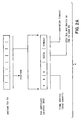
- Fig. 1 illustrates a block diagram of an interface structure according to an exemplary embodiment of the present invention.
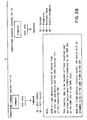
- Fig. 2 illustrates the command protocol when the device is located using its SCSI address, according to the exemplary embodiment of the invention.
- Fig. 3 illustrates the command protocol when the device is located using its slot address, according to the exemplary embodiment of the invention.
- Fig. 4 illustrates parallel SCSI concurrent maintenance in accordance with the exemplary embodiment of the invention.
- FIG. 1 illustrates a block diagram of an interface structure 100 according to an exemplary embodiment of the present invention, in a computer system with two PCI boards, each having two bridge circuits.
- the invention of course is not limited to this number of boards/circuits and this number was chosen merely to simplify illustration and explanation.
- Fig. 1 is a representation of an SPCN/PCIB IIC Interface, Physical Layer, that is, the physical interface between a system power controller, the system power control network SPCN, and each PCIB chip on each PCI Board in an enclosure or tower.
- the PCIB chips are exemplary PCI bridge circuits which were mentioned in the background section above.
- the PCI bridge circuits serve to couple system components, e.g., DASD input-output adapters processors and their adapters (IOPs and IOAs) to the host processor bus or system bus, which may also be a PCI bus.
- the IOP and IOA make up a DASD Ppcontroller.
- An IOP can control multiple IOAs and each IOA can source multiple SCSI buses.
- the DASDs are typically coupled to their IOA through an SCSI bus, as described earlier.
- Signalling and/or interlock mechanism 110 indicates/permits DASD concurrent maintenance.
- a system power control network processor 102 communicates with each bridge circuit 103A-103D on the PCI boards 105A and 105B, through a simple point-to-point connection 104A-104D, such as the industry standard I2C (IIC) serial bus.
- IIC industry standard I2C
- an analog multiplexer 106 may be provided along with a controller 107, e.g., an 8584 IC, to establish the connection to the SPCN processor 102.
- controller 107 e.g., an 8584 IC
- Each PCI bridge circuit (PCIB) 103A-103D includes, for example, a 256 byte address space which is readable and writable by SPCN and the IOPs located in slots under the PCI bridge.
- the PCI bridge circuit interface to SPCN is implemented with, for example, IIC slave support as a serial RAM device, SPCN providing IIC master capability.
- each PCIB to SPCN interface is a point-to-point connection with a single master and a single slave, however other configurations are possible within the spirit of the invention.
- the illustrated configuration advantageously provides a simple and effective way of accomplishing the objectives of the invention.
- Interface signals used implement a simple two-wire point-to-point IIC interface per PCI bridge chip (PCIB), providing data and clock signals for efficient communication between PCIB and SPCN.
- PCIB PCI bridge chip
- each bridge circuit (PCIB chip) 103A-103D is hardwired to a fixed IIC address according to the exemplary illustrated embodiment, only one PCIB chip 103A-103D per IIC bus 104A-104D may be connected to SPCN.
- the interface in an exemplary embodiment is implemented with a serial RAM IIC master/slave protocol, which is known to one skilled in the art and will not be described in detail here.
- RAM initialization is implemented at system start-up, so that after a power on reset, all RAM locations in the SPCN range are set to zeroes.
- the SPCN/PCIB IIC interface logical protocol is implemented such that PCIB provides slave function as a serial RAM to IIC master function in SPCN.
- SPCN initiates all communications via reads and writes to a selected range of serial RAM addresses where a fixed address range is assigned to each PCI bus slot under the PCIB PCI bridge.
- the PCI bridge can accommodate 8 local buses, i.e., slots or "functions", for any combination of up to 8 IOPs and IOAs.
- PCIB RAM usage i.e., how PCIB RAM is allocated, according to an exemplary embodiment of the invention.
- the address range 00-0F is allocated to the computer operating system to correlate PCI boards and Frame ID (SPCN Tower address) to the logical address of the particular Host bus connected to this bridge, for example.
- Range 10-1F provides 8 command/response register pairs for the interface from PCIB to SPCN, while range 20-2F provides 8 command/response register pairs for the interface from SPCN to PCIB.
- This RAM is not read/write, but operates set bit/clear bit per mask.
- Range 80-BF consists of 8-8 byte payloads for each command/response register pair in the interface from PCIB to SPCN, while range C0-FF consists of payloads for each command/response register pair in the interface from SPCN to PCIB. This is read/write RAM. Range 80-BF is therefore "downstream” i.e., PCIB to SPCN, while range C0-FF is "upstream” i.e., from SPCN to PCIB.
- command registers and eight response registers are allocated to the interface for communication in each direction, i.e., upstream and downstream. These registers are allocated with two pair per PCIB slot. One pair is used for downstream communication (PCIB to SPCN) and the other pair is used for upstream communication (SPCN to PCIB).
- PCIB to SPCN One pair is used for downstream communication
- SPCN to PCIB upstream communication
- the downstream path is used for DASD concurrent maintenance according to the invention.
- the upstream path could be used for various other operations not pertinent to the present invention.
- PCIB to SPCN command/response format is shown below illustrating how shared RAM is allocated to a separate communication for each possible slot under the PCIB bridge chip (bit 0 is the most significant bit):
- the exemplary SPCN to PCIB command response interface is like the PCIB to SPCN command response interface.
- the exemplary SPCN to PCIB command/response format is shown below: loaded by IOP after command processed and before bit 0 of respective Function command in 20-27 is cleared by the IOP.
- an input/output processor (IOP) in PCI slot Fn receives a request for concurrent maintenance on one of the devices (e.g., a DASD) it controls from the operating system.
- IOP input/output processor
- the IOP builds parameters, e.g., SCSI address, timeout, and loads the parameters in the read/write RAM payload allocated for PCIB function n. Then the IOP sets the command, e.g., hex '81' for an SCSI remove command, into the command byte location allocated to downstream interface for PCIB function n. The IOP starts a timer for the operation.
- SPCN is continually polling RAM locations x'10-17' to detect command from the IOPs. Commands are detected by a 1 in the high order bit of a command byte, for example. SPCN reads the payload location associated with Fn, and executes the concurrent maintenance operation.
- SPCN loads response status in the downstream interface response byte allocated to Fn.
- SPCN clears the high order bit of the downstream command register allocated to Fn using a write to the respective address in the range 40-47 (i.e., 4n). Clearing the command bit causes an interrupt to the IOP. If no response is received from SPCN within an operation timeout, the IOP clears the command byte high order bit to cancel the operation.
- the IOP After receiving an operating system request for concurrent maintenance on a specific device, the IOP builds the command which will be loaded in the appropriate payload and command register as described above.
- Figs. 2 and 3 illustrate this command format in the payload, and command and response registers.
- Fig. 2 illustrates the command protocol when the device is located using its SCSI address, according to the exemplary embodiment of the invention
- Fig. 3 illustrates the command protocol when the device is located using its slot address, according to the exemplary embodiment of the invention.
- the IOP Before the command can be loaded, causing SPCN to detect it and turn off power, the IOP must quiesce the SCSI bus to which the selected device (DASD) is connected.
- the SCSI bus is temporarily quiesced so that the act of powering the device (DASD) on and off, and the act of removal and installation, will not disturb other activity on the SCSI bus, and so that there is no potential for the insertion of a replacement device (DASD) to cause voltage transients that may also cause errors in other devices.
- the bus is quiesced for a matter of seconds and is limited because if bus activity is stopped too long, it will drive the operating system into error recovery which is of course undesirable. Consequently, both the IOP and SPCN time the operation, and that is the purpose of the time value "timeout" passed to SPCN in the commands illustrated.
- Fig. 4 illustrates parallel SCSI concurrent maintenance in accordance with the exemplary embodiment of the invention.
- SPCN 102 is connected to PCIB (PCI bridge chip) 103 having RAM 103M through which PCIB and SPCN communicate, as described above.
- the PCIB 103 is coupled by PCI bus 401 to PCI slots which contain one or more input/output adapters (IOAs, e.g., 402A) and associated input/output processor (IOP, e.g., 402P).
- IOAs input/output adapters
- IOP input/output processor
- the IOAs connect through backplane wiring or cables, e.g., SCSI buses 408, to peripheral devices 404, e.g., DASDs.
- item 408 represents a plurality of buses, e.g., three SCSI buses, leading from one IOA to a number of DASDs, e.g., five DASDs each.
- Power to the devices 404 is controlled by SPCN through device power control lines 406.
- an IOA e.g., 402A
- Fig. 4 illustrates a typical configuration, however, the invention is not limited to the particular architecture illustrated.
- the IOP loads the SCSI bus address, i.e., which of the 3 busses on an IOA, and the Device address into the indicated field "SCSI@" in the payload.
- SPCN 102 has built-in knowledge of the interconnections from the SCSI bus in each IOA slot to the respective device. SPCN 102 determines the IOA requesting service from the shared register space, by which command register contains a command. That is, a command in the register allocated to slot 4 (F4), for example, indicates the IOA 402A connected to the three buses 408 is requesting concurrent maintenance.
- the SCSI address in the payload indicates which bus, and which device on that bus. SPCN will translate that to determine the appropriate slot to control and monitor.
- the connections from every particular bus in each PCI slot must be fixed, either by board wiring or by restricting the cables to a fixed configuration. This is necessary so that the correct device is turned off/on.
- the IOP/IOA has knowledge itself of the device slot requiring service and it puts the slot address (SLOT@) directly in the payload.
- the method by which the IOP knows the slot address was the subject of the application referenced earlier, i.e., copending application serial number 08/971,687 (attorney docket number RO997-154-IBM-108).
- SPCN told the DASD devices themselves, or a special SCSI target processor, called an SES device or processor, of the slot addresses of each device.
- the IOP communicated with each DASD device or SES device on each SCSI bus and retrieved from that device its slot address directly. This allowed the IOP to correlate SCSI BUS/Device address to slot address directly. This translation was unknown to SPCN and it was not necessary for SPCN to know about the translation because the IOP would directly ask for maintenance by DASD slot address directly.
- SPCN detects the SCSI remove command, for example, it turns power off to the device, signals and/or unlocks the device with block 110, and watches for the device to be removed. If the device is removed, a successful response is returned. If the device is not removed before a timeout expires, then an unsuccessful response is returned. The IOP releases the bus, and the DASD operation resumes on this bus.
- the SCSI install operation is the reverse of the remove operation.
- the SPCN can also use the PCIB RAM to pass device location, by enclosure ("frame” or “tower") and backplane, e.g., PCI backplane, as well as the PCI slot on the PCI backplane to the operating system.
- SPCN will assign the frame and backplane a unique number at start-up, and will reassign such when frames or backplanes are added or removed.
- PCI slot location is according to PCI slot address assignment within the PCI architecture. The details of this mechanism are not necessary for an understanding of this invention, and are the subject matter of copending application serial number 08/971,687 (attorney docket number RO997-154-IBM-108) mentioned above.
- the SPCN have some way of uniquely identifying each device in the system, e.g., by its actual physical location, in order to coordinate the concurrent maintenance thereof.
- an IOA can provide one or more SCSI buses, and each SCSI bus could have a plurality of DASDs connected thereon, the SCSI bus, and the device number/device slot on the SCSI bus also needs to be known by SPCN, and this information could also be gathered at start-up by SPCN.
- SPCN can map physical location of a device from the SCSI bus and SCSI device, and the slot location of the IOA requesting concurrent maintenance, for example. For the purposes of the invention, it is assumed that some way for the system power controller to identify devices requesting concurrent maintenance exists, but the invention is not necessarily limited to the particular way this is accomplished.
- a single SPCN controller can advantageously control all the devices within an enclosure, i.e., a frame or tower, resulting in a substantial cost reduction over other arrangements using system enclosure services (SES) processors.
- SES system enclosure services
- the number of DASDs connected to a single SCSI bus is limited, for example, to five DASDs.
- An enclosure containing forty-five DASDs, for example, would therefore have nine SCSI buses.
- nine such processors would be required for the enclosure.
- the functions performed by these nine SES processors are performed by one SPCN controller. This is illustrated in Fig. 4.
- Each of the three illustrated IOA/IOP combinations controls three SCSI buses, e.g., SCSI buses 408.
- SCSI buses e.g., SCSI buses 408.
- Each of the SCSI buses is in turn coupled to five of the DASDs in the nine banks of DASDs 404. In this exemplary enclosure arrangement therefore, forty-five DASDs are driven with nine SCSI buses and three IOA/IOP combinations.
- the three IOA/IOP combinations are connected to the one PCI bridge chip (PCIB) 103 through the PCI bus 401.
- PCIB PCI bridge chip
- one SPCN controller 102 can control concurrent maintenance for the forty-five DASDs in the enclosure communicating with all the IOA/IOP combinations through a single interface 104 to the PCI bridge (PCIB) 103.
- PCIB PCI bridge
- the invention is not limited to a mid-range or high-end computer system, but could have applicability to any electrical system. While described in the context of concurrent maintenance of DASDs on SCSI buses, concurrent maintenance of any other type of system component could of course be accomplished with the invention.
- the exemplary embodiment described above used a system power control network (SPCN), however, any system power controller or system enclosure services device (SES) with similar capabilities could be substituted therefore.
- SPCN system power control network
- SES system enclosure services device
- the embodiment described above included a first communications path to the DASD through the SCSI bus from the input-output adapter (IOA) which was connected by a PCI slot to a PCI bus on a PCI backplane having a PCI bridge circuit (PCIB) bridging the backplane PCI bus to a system or host PCI bus, however, the invention is not limited to this particular first communications path configuration.
- IOA input-output adapter
- PCIB PCI bridge circuit
- the described embodiment uses a second communications path from SPCN to an PCIB chip RAM, through which concurrent maintenance information is communicated between the IOA and the SPCN, however, the invention is not limited to this particular second communications path.
- the invention comprehends any second communications path which provides the advantages mentioned above, e.g., the first communications path between the device needing service and its adapter is not required to be operational to perform concurrent maintenance operations and non-compliance with standards for the first communications path are avoided.
- the second communication paths from a number of bridge chips are multiplexed, however the invention is not limited to this particular implementation. All of the bridge chips could be connected to a single interface, each chip having a unique address for communication therewith.
Landscapes
- Engineering & Computer Science (AREA)
- Theoretical Computer Science (AREA)
- Physics & Mathematics (AREA)
- General Engineering & Computer Science (AREA)
- General Physics & Mathematics (AREA)
- Power Sources (AREA)
Applications Claiming Priority (2)
| Application Number | Priority Date | Filing Date | Title |
|---|---|---|---|
| US90387 | 1998-06-04 | ||
| US09/090,387 US6199130B1 (en) | 1998-06-04 | 1998-06-04 | Concurrent maintenance for PCI based DASD subsystem with concurrent maintenance message being communicated between SPCN (system power control network) and I/O adapter using PCI bridge |
Publications (2)
| Publication Number | Publication Date |
|---|---|
| EP0962863A2 true EP0962863A2 (de) | 1999-12-08 |
| EP0962863A3 EP0962863A3 (de) | 2002-10-02 |
Family
ID=22222566
Family Applications (1)
| Application Number | Title | Priority Date | Filing Date |
|---|---|---|---|
| EP99304027A Withdrawn EP0962863A3 (de) | 1998-06-04 | 1999-05-25 | Gleichzeitige DASD Wartung für ein auf PCI-Bus gestütztes DASD Subsystem |
Country Status (2)
| Country | Link |
|---|---|
| US (1) | US6199130B1 (de) |
| EP (1) | EP0962863A3 (de) |
Families Citing this family (45)
| Publication number | Priority date | Publication date | Assignee | Title |
|---|---|---|---|---|
| US6427176B1 (en) * | 1999-03-04 | 2002-07-30 | International Business Machines Corporation | Method and apparatus for maintaining system labeling based on stored configuration labeling information |
| US6854026B1 (en) | 1999-12-29 | 2005-02-08 | General Electric Company | Methods and systems for interfacing small devices to computer networks |
| US6519663B1 (en) * | 2000-01-12 | 2003-02-11 | International Business Machines Corporation | Simple enclosure services (SES) using a high-speed, point-to-point, serial bus |
| US6581121B1 (en) * | 2000-02-25 | 2003-06-17 | Telica, Inc. | Maintenance link system and method |
| US7036033B1 (en) * | 2001-01-04 | 2006-04-25 | 3Pardata, Inc. | Disk enclosure with multiplexers for connecting 12C buses in multiple power domains |
| US7200144B2 (en) * | 2001-10-18 | 2007-04-03 | Qlogic, Corp. | Router and methods using network addresses for virtualization |
| GB0219570D0 (en) * | 2002-08-22 | 2002-10-02 | Ibm | Disk drive arrangement, enclosure, adapter and method |
| US7394445B2 (en) | 2002-11-12 | 2008-07-01 | Power-One, Inc. | Digital power manager for controlling and monitoring an array of point-of-load regulators |
| US6949916B2 (en) | 2002-11-12 | 2005-09-27 | Power-One Limited | System and method for controlling a point-of-load regulator |
| US7051140B2 (en) | 2002-11-13 | 2006-05-23 | International Business Machines Corporation | Connector that enables aggregation of independent system resources across PCI/PCI-X bus and interlocked method for aggregating independent system resources across PCI/PCI-X bus |
| US7456617B2 (en) * | 2002-11-13 | 2008-11-25 | Power-One, Inc. | System for controlling and monitoring an array of point-of-load regulators by a host |
| US6833691B2 (en) * | 2002-11-19 | 2004-12-21 | Power-One Limited | System and method for providing digital pulse width modulation |
| US7737961B2 (en) * | 2002-12-21 | 2010-06-15 | Power-One, Inc. | Method and system for controlling and monitoring an array of point-of-load regulators |
| US7673157B2 (en) | 2002-12-21 | 2010-03-02 | Power-One, Inc. | Method and system for controlling a mixed array of point-of-load regulators through a bus translator |
| US7836322B2 (en) * | 2002-12-21 | 2010-11-16 | Power-One, Inc. | System for controlling an array of point-of-load regulators and auxiliary devices |
| US7249267B2 (en) * | 2002-12-21 | 2007-07-24 | Power-One, Inc. | Method and system for communicating filter compensation coefficients for a digital power control system |
| US7743266B2 (en) * | 2002-12-21 | 2010-06-22 | Power-One, Inc. | Method and system for optimizing filter compensation coefficients for a digital power control system |
| US7882372B2 (en) * | 2002-12-21 | 2011-02-01 | Power-One, Inc. | Method and system for controlling and monitoring an array of point-of-load regulators |
| US7266709B2 (en) | 2002-12-21 | 2007-09-04 | Power-One, Inc. | Method and system for controlling an array of point-of-load regulators and auxiliary devices |
| US7373527B2 (en) * | 2002-12-23 | 2008-05-13 | Power-One, Inc. | System and method for interleaving point-of-load regulators |
| US7023190B2 (en) * | 2003-02-10 | 2006-04-04 | Power-One, Inc. | ADC transfer function providing improved dynamic regulation in a switched mode power supply |
| US7710092B2 (en) * | 2003-02-10 | 2010-05-04 | Power-One, Inc. | Self tracking ADC for digital power supply control systems |
| US6988158B2 (en) * | 2003-02-26 | 2006-01-17 | Inventec Corporation | Hot plug circuit for enclosure management systems used to manage sub-systems and method thereof |
| US20040193770A1 (en) * | 2003-03-13 | 2004-09-30 | Whiteman Jason W. | Communicating information in a computer system |
| US6936999B2 (en) * | 2003-03-14 | 2005-08-30 | Power-One Limited | System and method for controlling output-timing parameters of power converters |
| US7080265B2 (en) * | 2003-03-14 | 2006-07-18 | Power-One, Inc. | Voltage set point control scheme |
| US7653757B1 (en) * | 2004-08-06 | 2010-01-26 | Zilker Labs, Inc. | Method for using a multi-master multi-slave bus for power management |
| US7685320B1 (en) * | 2003-04-11 | 2010-03-23 | Zilker Labs, Inc. | Autonomous sequencing and fault spreading |
| US7506179B2 (en) * | 2003-04-11 | 2009-03-17 | Zilker Labs, Inc. | Method and apparatus for improved DC power delivery management and configuration |
| US7793005B1 (en) * | 2003-04-11 | 2010-09-07 | Zilker Labs, Inc. | Power management system using a multi-master multi-slave bus and multi-function point-of-load regulators |
| US7372682B2 (en) * | 2004-02-12 | 2008-05-13 | Power-One, Inc. | System and method for managing fault in a power system |
| US7141956B2 (en) * | 2005-03-18 | 2006-11-28 | Power-One, Inc. | Digital output voltage regulation circuit having first control loop for high speed and second control loop for high accuracy |
| US7554310B2 (en) * | 2005-03-18 | 2009-06-30 | Power-One, Inc. | Digital double-loop output voltage regulation |
| US7239115B2 (en) * | 2005-04-04 | 2007-07-03 | Power-One, Inc. | Digital pulse width modulation controller with preset filter coefficients |
| US7327149B2 (en) * | 2005-05-10 | 2008-02-05 | Power-One, Inc. | Bi-directional MOS current sense circuit |
| US8515342B2 (en) * | 2005-10-12 | 2013-08-20 | The Directv Group, Inc. | Dynamic current sharing in KA/KU LNB design |
| US7676622B2 (en) * | 2007-06-07 | 2010-03-09 | International Business Machines Corporation | System and method for improved bus communication |
| US7834613B2 (en) * | 2007-10-30 | 2010-11-16 | Power-One, Inc. | Isolated current to voltage, voltage to voltage converter |
| US20090225618A1 (en) * | 2008-03-05 | 2009-09-10 | Inventec Corporation | Power management module for memory module |
| US8120203B2 (en) * | 2008-07-18 | 2012-02-21 | Intersil Americas Inc. | Intelligent management of current sharing group |
| US8237423B2 (en) | 2008-07-18 | 2012-08-07 | Intersil Americas Inc. | Active droop current sharing |
| US8239597B2 (en) * | 2008-07-18 | 2012-08-07 | Intersil Americas Inc. | Device-to-device communication bus for distributed power management |
| US8120205B2 (en) * | 2008-07-18 | 2012-02-21 | Zilker Labs, Inc. | Adding and dropping phases in current sharing |
| US8271697B2 (en) * | 2009-09-29 | 2012-09-18 | Micron Technology, Inc. | State change in systems having devices coupled in a chained configuration |
| US11892971B2 (en) | 2019-03-01 | 2024-02-06 | International Business Machines Corporation | Non-disruptive repair of enclosure controller components |
Citations (2)
| Publication number | Priority date | Publication date | Assignee | Title |
|---|---|---|---|---|
| US5586250A (en) * | 1993-11-12 | 1996-12-17 | Conner Peripherals, Inc. | SCSI-coupled module for monitoring and controlling SCSI-coupled raid bank and bank environment |
| US5815647A (en) * | 1995-11-02 | 1998-09-29 | International Business Machines Corporation | Error recovery by isolation of peripheral components in a data processing system |
Family Cites Families (15)
| Publication number | Priority date | Publication date | Assignee | Title |
|---|---|---|---|---|
| CH637228A5 (fr) * | 1980-03-27 | 1983-07-15 | Willemin Machines Sa | Dispositif de commande d'une machine ou d'une installation. |
| US4901232A (en) * | 1983-05-19 | 1990-02-13 | Data General Corporation | I/O controller for controlling the sequencing of execution of I/O commands and for permitting modification of I/O controller operation by a host processor |
| US5117430A (en) | 1991-02-08 | 1992-05-26 | International Business Machines Corporation | Apparatus and method for communicating between nodes in a network |
| US5774640A (en) * | 1991-10-21 | 1998-06-30 | Tandem Computers Incorporated | Method and apparatus for providing a fault tolerant network interface controller |
| JPH0821015B2 (ja) * | 1992-01-20 | 1996-03-04 | インターナショナル・ビジネス・マシーンズ・コーポレイション | コンピュータならびにそのシステム再構成化装置および方法 |
| JP2691140B2 (ja) * | 1994-09-28 | 1997-12-17 | インターナショナル・ビジネス・マシーンズ・コーポレイション | 情報処理装置及びその制御方法 |
| US5793993A (en) * | 1995-01-26 | 1998-08-11 | General Magic, Inc. | Method for transmitting bus commands and data over two wires of a serial bus |
| JPH096718A (ja) * | 1995-06-16 | 1997-01-10 | Toshiba Corp | ポータブルコンピュータシステム |
| US5793987A (en) * | 1996-04-18 | 1998-08-11 | Cisco Systems, Inc. | Hot plug port adapter with separate PCI local bus and auxiliary bus |
| US5875310A (en) * | 1996-05-24 | 1999-02-23 | International Business Machines Corporation | Secondary I/O bus with expanded slot capacity and hot plugging capability |
| US5890004A (en) * | 1996-12-30 | 1999-03-30 | Intel Corporation | Method and apparatus for signaling power management events between two devices |
| US5875308A (en) * | 1997-06-18 | 1999-02-23 | International Business Machines Corporation | Peripheral component interconnect (PCI) architecture having hot-plugging capability for a data-processing system |
| US5935252A (en) * | 1997-08-18 | 1999-08-10 | International Business Machines Corporation | Apparatus and method for determining and setting system device configuration relating to power and cooling using VPD circuits associated with system devices |
| US6044411A (en) * | 1997-11-17 | 2000-03-28 | International Business Machines Corporation | Method and apparatus for correlating computer system device physical location with logical address |
| US6014319A (en) * | 1998-05-21 | 2000-01-11 | International Business Machines Corporation | Multi-part concurrently maintainable electronic circuit card assembly |
-
1998
- 1998-06-04 US US09/090,387 patent/US6199130B1/en not_active Expired - Fee Related
-
1999
- 1999-05-25 EP EP99304027A patent/EP0962863A3/de not_active Withdrawn
Patent Citations (2)
| Publication number | Priority date | Publication date | Assignee | Title |
|---|---|---|---|---|
| US5586250A (en) * | 1993-11-12 | 1996-12-17 | Conner Peripherals, Inc. | SCSI-coupled module for monitoring and controlling SCSI-coupled raid bank and bank environment |
| US5815647A (en) * | 1995-11-02 | 1998-09-29 | International Business Machines Corporation | Error recovery by isolation of peripheral components in a data processing system |
Non-Patent Citations (2)
| Title |
|---|
| "DIRECT ACCESS STORAGE DEVICE (DASD) CONCURRENT MAINTENANCE" IBM TECHNICAL DISCLOSURE BULLETIN, IBM CORP. NEW YORK, US, vol. 33, no. 8, 1991, pages 223-227, XP000106938 ISSN: 0018-8689 * |
| ANONYMOUS: "Input/Output Processor/System Power Control Network Diagnostic Interface" IBM TECHNICAL DISCLOSURE BULLETIN, vol. 39, no. 1, 1 January 1996 (1996-01-01), pages 89-90, XP002204505 New York, US * |
Also Published As
| Publication number | Publication date |
|---|---|
| US6199130B1 (en) | 2001-03-06 |
| EP0962863A3 (de) | 2002-10-02 |
Similar Documents
| Publication | Publication Date | Title |
|---|---|---|
| US6199130B1 (en) | Concurrent maintenance for PCI based DASD subsystem with concurrent maintenance message being communicated between SPCN (system power control network) and I/O adapter using PCI bridge | |
| US6044411A (en) | Method and apparatus for correlating computer system device physical location with logical address | |
| CN100541444C (zh) | 多主板系统之管理系统 | |
| CN1124551C (zh) | 用于热插入处理器到数据处理系统中的方法和系统 | |
| US6070207A (en) | Hot plug connected I/O bus for computer system | |
| US5499346A (en) | Bus-to-bus bridge for a multiple bus information handling system that optimizes data transfers between a system bus and a peripheral bus | |
| US6735660B1 (en) | Sideband signal transmission between host and input/output adapter | |
| US6134579A (en) | Semaphore in system I/O space | |
| US20080259555A1 (en) | Modular blade server | |
| US6158015A (en) | Apparatus for swapping, adding or removing a processor in an operating computer system | |
| US6957288B2 (en) | Embedded control and monitoring of hard disk drives in an information handling system | |
| CN114579500B (zh) | 用于高速数据通讯的系统、中介件及方法 | |
| CN213365380U (zh) | 一种服务器主板及服务器 | |
| CN112000501A (zh) | 一种多节点分区服务器访问i2c设备的管理系统 | |
| US6108732A (en) | Method for swapping, adding or removing a processor in an operating computer system | |
| CN115167629A (zh) | 一种双路服务器cpu主板 | |
| WO1993015459A1 (en) | Live insertion of computer modules | |
| US6205503B1 (en) | Method for the hot swap and add of input/output platforms and devices | |
| CN100414526C (zh) | 自动调整总线宽度的方法及装置 | |
| CN210627095U (zh) | 一种通用包含各种总线主板的加固计算机 | |
| AU768503B2 (en) | Fault tolerant virtual VMEbus backplane design | |
| CN100395744C (zh) | 实现中央控制单元对单板集中控制的方法和系统 | |
| CN112306938A (zh) | 一种ocp卡和多主机卡的热插拔方法及装置 | |
| US7000053B2 (en) | Computer system having a hot swappable hot swap controller | |
| CN117349212A (zh) | 一种服务器主板及其固态硬盘插入检测方法 |
Legal Events
| Date | Code | Title | Description |
|---|---|---|---|
| PUAI | Public reference made under article 153(3) epc to a published international application that has entered the european phase |
Free format text: ORIGINAL CODE: 0009012 |
|
| AK | Designated contracting states |
Kind code of ref document: A2 Designated state(s): AT BE CH CY DE DK ES FI FR GB GR IE IT LI LU MC NL PT SE |
|
| AX | Request for extension of the european patent |
Free format text: AL;LT;LV;MK;RO;SI |
|
| PUAL | Search report despatched |
Free format text: ORIGINAL CODE: 0009013 |
|
| RIC1 | Information provided on ipc code assigned before grant |
Free format text: 7G 06F 11/20 A, 7G 06F 11/273 B, 7G 06F 13/40 B, 7G 06F 1/26 B, 7G 06F 1/32 B |
|
| AK | Designated contracting states |
Kind code of ref document: A3 Designated state(s): AT BE CH CY DE DK ES FI FR GB GR IE IT LI LU MC NL PT SE |
|
| AX | Request for extension of the european patent |
Free format text: AL;LT;LV;MK;RO;SI |
|
| RTI1 | Title (correction) |
Free format text: DASD CONCURRENT MAINTENANCE FOR A PCI BASED DASD SUBSYSTEM |
|
| 17P | Request for examination filed |
Effective date: 20030315 |
|
| 17Q | First examination report despatched |
Effective date: 20030502 |
|
| AKX | Designation fees paid |
Designated state(s): DE FR GB |
|
| STAA | Information on the status of an ep patent application or granted ep patent |
Free format text: STATUS: THE APPLICATION HAS BEEN WITHDRAWN |
|
| 18W | Application withdrawn |
Effective date: 20070326 |