EP0956560B1 - Leserverstärkerschaltung - Google Patents
Leserverstärkerschaltung Download PDFInfo
- Publication number
- EP0956560B1 EP0956560B1 EP97953923A EP97953923A EP0956560B1 EP 0956560 B1 EP0956560 B1 EP 0956560B1 EP 97953923 A EP97953923 A EP 97953923A EP 97953923 A EP97953923 A EP 97953923A EP 0956560 B1 EP0956560 B1 EP 0956560B1
- Authority
- EP
- European Patent Office
- Prior art keywords
- output
- current
- circuit
- value
- sense amplifier
- Prior art date
- Legal status (The legal status is an assumption and is not a legal conclusion. Google has not performed a legal analysis and makes no representation as to the accuracy of the status listed.)
- Expired - Lifetime
Links
- 229910021420 polycrystalline silicon Inorganic materials 0.000 claims description 9
- 229920005591 polysilicon Polymers 0.000 claims 1
- 230000015654 memory Effects 0.000 abstract description 36
- 210000004027 cell Anatomy 0.000 description 28
- 239000004065 semiconductor Substances 0.000 description 7
- 230000006870 function Effects 0.000 description 4
- 238000011156 evaluation Methods 0.000 description 2
- 238000000034 method Methods 0.000 description 2
- 239000013643 reference control Substances 0.000 description 2
- 210000000352 storage cell Anatomy 0.000 description 2
- 239000000758 substrate Substances 0.000 description 2
- 238000003491 array Methods 0.000 description 1
- 230000003111 delayed effect Effects 0.000 description 1
- 238000001514 detection method Methods 0.000 description 1
- 229910052710 silicon Inorganic materials 0.000 description 1
- 239000010703 silicon Substances 0.000 description 1
- 230000007704 transition Effects 0.000 description 1
Images



Classifications
-
- G—PHYSICS
- G11—INFORMATION STORAGE
- G11C—STATIC STORES
- G11C11/00—Digital stores characterised by the use of particular electric or magnetic storage elements; Storage elements therefor
- G11C11/56—Digital stores characterised by the use of particular electric or magnetic storage elements; Storage elements therefor using storage elements with more than two stable states represented by steps, e.g. of voltage, current, phase, frequency
-
- G—PHYSICS
- G11—INFORMATION STORAGE
- G11C—STATIC STORES
- G11C11/00—Digital stores characterised by the use of particular electric or magnetic storage elements; Storage elements therefor
- G11C11/56—Digital stores characterised by the use of particular electric or magnetic storage elements; Storage elements therefor using storage elements with more than two stable states represented by steps, e.g. of voltage, current, phase, frequency
- G11C11/5621—Digital stores characterised by the use of particular electric or magnetic storage elements; Storage elements therefor using storage elements with more than two stable states represented by steps, e.g. of voltage, current, phase, frequency using charge storage in a floating gate
-
- G—PHYSICS
- G11—INFORMATION STORAGE
- G11C—STATIC STORES
- G11C11/00—Digital stores characterised by the use of particular electric or magnetic storage elements; Storage elements therefor
- G11C11/56—Digital stores characterised by the use of particular electric or magnetic storage elements; Storage elements therefor using storage elements with more than two stable states represented by steps, e.g. of voltage, current, phase, frequency
- G11C11/5621—Digital stores characterised by the use of particular electric or magnetic storage elements; Storage elements therefor using storage elements with more than two stable states represented by steps, e.g. of voltage, current, phase, frequency using charge storage in a floating gate
- G11C11/5642—Sensing or reading circuits; Data output circuits
-
- G—PHYSICS
- G11—INFORMATION STORAGE
- G11C—STATIC STORES
- G11C2211/00—Indexing scheme relating to digital stores characterized by the use of particular electric or magnetic storage elements; Storage elements therefor
- G11C2211/56—Indexing scheme relating to G11C11/56 and sub-groups for features not covered by these groups
- G11C2211/564—Miscellaneous aspects
- G11C2211/5645—Multilevel memory with current-mirror arrangements
-
- G—PHYSICS
- G11—INFORMATION STORAGE
- G11C—STATIC STORES
- G11C7/00—Arrangements for writing information into, or reading information out from, a digital store
- G11C7/06—Sense amplifiers; Associated circuits, e.g. timing or triggering circuits
Definitions
- the present invention relates, in general, to semiconductor devices, and more particularly to a sense circuit suitable for use in semiconductor devices.
- the prior circuits generally utilise voltage sensing amplifiers that sense the voltage value of information in each cell of the memory array. When the memory cell read, it takes along time for the voltage to charge capacitance's coupled to the memory cell thereby requiring a long read cycle for the memory array.
- a sense circuit that consumes a small semiconductor area, that can sense more than two states that are stored within a memory cell, and that results in a fast read cycle for the memory array or memory cells.
- FIG. 1 schematically illustrates a sense circuit 10 that is suitable for use with memory cells or memory arrays that stores multiple states within each cell [not shown].
- the memory cell associated with circuit 10 typically utilises one erase state and three programmed states in order to store four different states within each memory cell.
- Circuit 10 includes a first or most significant current sense amplifier 11 and an associated most significant or first output latch 13 that provides a digital signal on a most significant or first output 23 it represents the state detected by amplifier 11 circuit 10 also includes a least significant or second current sense amplifier 12 and associated least significant or second output latch 14 that has a least significant or second output 24 that stores a digital value representing the state detected by amplifier 12.
- An output cell or portion of a memory array is connected to a current signal input 17 of circuit 10.
- the current signal applied to input 17 has one of four different values of current depending on the state stored within the memory cell or memory array.
- the value of this current is detected and decoded by circuit 10 which provides two digital outputs comprising a most significant output bit 23 and a least significant output bit 24 that represent the four digital states stored in the memory cell.
- a read cycle for a cell within the memory array is composed of four phases.
- a most significant sense output 20 is held low in order to prevent affecting latch 13 by a most significant pulldown transistor 56 which is enabled by a most significant sense output disabled signal 21.
- a sense amp enable 18 is held high in order to disable sense amp 12 and to facilitate disabling sense amp 11. Because a next bit control 19 is low, transistor 57 is disabled thereby disabling amplifier 11. Signal 18 disables transistor 58 thereby disabling amplifier 12. As enabled 18 goes to a high state, present circuit 27 generates a pulse that presets latches 13 and 14 to a high state so that a most significant output bit 23 and a least significant output bit 24 each have a high state.
- a most significant sense output disable 21 becomes low disabling transistor 56 thereby providing an output signal from amplifier 11 on output 20 and presenting the value of output 20 to latch 13 thereby ensuring that output bit 23 of latch 13 represents the state of output 20.
- the value of the current applied to input 17 is compared to three different reference current values which are applied to reference current input 26.
- the value applied to input 17 is compared to a first reference current value. If the value of the current applied to input 17 is greater than the first reference current value [i.e. output bit 23 is high] a second current value that is greater than the first current value will be applied to input 26 during the evaluate LSB phase in order to determine the state of output bit 24. however, if the value of the signal applied to input 17 is less than the first reference current, a third reference current value that is less than the first reference current value will be applied to input 26 in order to determine the state of bit 24.
- the value of the current applied to input 17 is applied to amplifier 11 by transistor 59 and mirrored to amplifier 12 by transistors 59 and 66 which function as a current mirror. Additionally, the value of the reference current applied to input 26 is applied to amplifier 11 by transistor 67 and mirrored to amplifier 12 by transistor 67 and 68.
- next bit control 19 goes high which disables amplifier 11 by disabling transistor 57, freezes the state of latch 13 by disabling transistor 66, and releases output 25 of amplifier 12 by disabling transistor 64 through delayed circuit 16 as will be seen hereinafter, either a second reference current value or a third reference current value is applied to input 26, and coupled to amplifier 12 in order to determine the state of output bit 24. If the value of the current applied to input 17 is greater than the value of the reference current applied to input 26, output 25 of amplifier 12 goes high thereby causing output 24 to go low, however, if the value of the current applied to input 17 is less than the value of the reference current applied to input 26 output 25 goes high and latch 14 remains preset so that output 24 also stays high. Consequently, the digital state of outputs 23 and 24 represent one of the four voltage value states that were stored on the bit cell.
- control 19 and disable 21 both go low thereby beginning a fourth phase of the read cycle which is used to discharge a bit line [not shown] and ending the four phases of the read cycle utilised to read or determine the value of the voltage stored on the bit cell of a memory array.
- FIG. 2 schematically illustrates a reference current circuit utilised to provide one of three reference current values to input 26 of circuit 10 shown in FIG. 1. Similar elements within Fig. 2 and FIG. 1 have the same reference numbers.
- Reference current circuit 30 has a voltage input [Vin]that is applied to a voltage supply circuit 31, [for example a zenor diode].
- Circuit 31 has a output 53 that is applied to a high precision voltage divider 32.
- divider 32 has six resistors which divide the voltage applied to input 53 and provides six reference voltages to high voltage mugs 33.
- Multiplexer 33 has a read control input 59 that selects three read reference voltages from the six voltages provided by divider 32. The value of most significant output bit 23 is also applied to mugs 33 in order to determine which of the three currents should be applied to outputs 34, 36 and 37 of multiplexer 33.
- Divider 32 converts the voltage applied to input 53 from a voltage value to six current values that are applied to multiplexer 33.
- the first output current is applied to output 35 and to the gate of a transistor 49 which is part of a select circuit 41 that is utilised to select the first referenced current that is applied to input 26.
- Output 36 is coupled to the gate of transistor 49.
- Transistor 49 has a double poly-silicon layer gate and is constructed in the same manner as the storage transistor utilised in the storage cell of the memory array. Both poly-layers of transistor 49 are shorted together so that transistor 49 functions as a normal ordinary transistor. Because transistor 49 is constructed in a similar manner than a storage cell transistor, the reference current applied to output 42 of select circuit 41 tracks the signal current provided by the cells so that process variations do not affect the accuracy of circuit 10.
- Transistor 49 has a source coupled to ground or a voltage return and a drain coupled to a source of a select transistor 48.
- a gate of transistor 48 is coupled to a first reference control input 72, and a drain is connected to an output 42 of circuit 41 which is coupled to input 26 via a matching load transistor 54.
- the second reference current supplied by multiplexer 33 is applied to a transistor 47 and is similar to transistor 49.
- Transistor 47 is part of a reference cell 38 that is similar to reference cell 41.
- Cell 38 has a select transistor 46 having a gate that is coupled to second reference control input 73 that is used to select the second reference current to input 26.
- a third reference cell 43 has a compensation transistor 52 that has a gate connected to output 37 of mugs 33 in order to receive the third reference current.
- Transistor 52 is constructed and functions similarly to transistor 49.
- Cell 43 also has a select transistor 51 that has a gate coupled to a third control input 71 that functions to select the third reference current coupled to input 26.
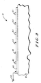
- FIG. 3 illustrates an enlarged cross-sectional portion of voltage divider 32 shown in FIG. 2. Similar elements are indicated by the same reference numbers.
- Divider 32 is formed on a substrate 61 and includes a layer of poly-silicon 62 that is formed on substrate 61. One end of layer 62 is connected to input 53. Periodically spaced thereafter are taps or electrical connection points 63 that are spaced at the same interval in order to create six resistors of equal value.
- divider 32 is a strain of poly-silicon with taps spaced along the poly-silicon string. Poly-silicon is utilised for the resistors because poly-silicon is very stable with temperature which helps ensure that the reference currents provided by divider 32 are very stable with temperature. Additionally, poly-silicon has a high resistance so that divider 32 minimises the amount of current and power dissipated by divider 32.
- FIG. 4 Schematically illustrates a smart card or personal data carrier that utilises circuit 10 and circuit 30.
- Carrier 200 includes a carrier envelope, such as plastic, 203 which encapsulates a control element 201, for example a micro-computer unit.
- Control unit 201 typically has a memory array 202 which is coupled to circuit 10 which in turn utilises circuit 30. Because of the advantages provided by circuits 10 and 30, unit 201 utilises a small area and provides rapid operation which increases the carrier 200 maybe utilised.
Landscapes
- Engineering & Computer Science (AREA)
- Computer Hardware Design (AREA)
- Read Only Memory (AREA)
Claims (6)
- Leseschaltung (10), die Folgendes umfasst:wobei der Referenzstrom vor dem Zeitabschnitt einen ersten Wert hat und während des Zeitabschnitts einen zweiten Wert hat, der von dem ersten Wert verschieden ist; und eine Einrichtung zum Auswählen des Referenzstromwertes in Abhängigkeit von dem ersten digitalen Ausgang.einen ersten Stromspiegel-Leseverstärker (11, 59, 67), der so geschaltet ist, dass er einen Signalstrom und einen Referenzstrom empfängt, wobei der erste Spiegelstrom-Leseverstärker einen ersten Ausgang hat;ein erstes Ausgangslatch (13), das so geschaltet ist, dass es den ersten Ausgang empfängt, wobei das erste Ausgangslatch einen ersten digitalen Ausgang (23) hat;einen zweiten Stromspiegel-Leseverstärker (12, 59, 67), der so geschaltet ist, dass er den Signalstrom und den Referenzstrom empfängt, wobei der zweite Stromspiegel-Leseverstärker einen zweiten Ausgang hat, wobei der erste Stromspiegel-Leseverstärker während eines Zeitabschnitts gesperrt ist, in dem der zweiten Stromspiegel-Leseverstärker aktiviert ist; undein zweites Ausgangslatch (14), das so geschaltet ist, dass es den zweiten Ausgang empfängt, wobei das zweite Ausgangslatch einen zweiten digitalen Ausgang (24) hat;
- Leseschaltung (10) nach Anspruch 1, die ferner eine Referenzstromschaltung (30) mit drei Referenzstromausgängen (34, 36, 37) umfasst, wobei ein erster Referenzstromausgang mit dem ersten Stromspiegel-Leseverstärker (11, 59, 67) durch eine erste Wählschaltung (41) verbunden ist und der zweite Stromspiegel-Leseverstärker (12, 59, 67) mit einem zweiten Referenzstromausgang durch eine zweite Wählschaltung (38) oder mit einem dritten Referenzstromausgang durch eine dritte Wählschaltung (43) verbunden ist.
- Leseschaltung (10) nach Anspruch 2, bei der die erste, die zweite und die dritte Wählschaltung (38, 41, 43) jeweils einen Polysiliciumtransistor mit einem Gate umfasst, bei dem eine Poly-1-Schicht verwendet wird.
- Leseschaltung (10) nach Anspruch 2 oder 3, bei der der Wert des ersten digitalen Ausgangs bestimmt, ob der zweite oder der dritte Referenzstromausgang mit dem zweiten Stromspiegel-Leseverstärker (12, 59, 67) verbunden wird.
- Leseschaltung (10) nach Anspruch 1, bei der ein Ausgangswert des zweiten digitalen Ausgangs während einer Zeit eingefroren wird, in der ein Ausgangswert des ersten digitalen Ausgangs aktiviert ist, und der Ausgangswert des ersten digitalen Ausgangs während einer Zeit eingefroren wird, in der der Ausgangswert des zweiten digitalen Ausgangs aktiviert ist.
- Tragbarer Datenträger (200) mit der Leseschaltung (10) nach Anspruch 1.
Applications Claiming Priority (3)
| Application Number | Priority Date | Filing Date | Title |
|---|---|---|---|
| GB9701858 | 1997-01-30 | ||
| GB9701858A GB2321736B (en) | 1997-01-30 | 1997-01-30 | Sense amplifier circuit |
| PCT/EP1997/007294 WO1998034232A1 (en) | 1997-01-30 | 1997-12-23 | Sense amplifier circuit |
Publications (2)
| Publication Number | Publication Date |
|---|---|
| EP0956560A1 EP0956560A1 (de) | 1999-11-17 |
| EP0956560B1 true EP0956560B1 (de) | 2003-12-03 |
Family
ID=10806782
Family Applications (1)
| Application Number | Title | Priority Date | Filing Date |
|---|---|---|---|
| EP97953923A Expired - Lifetime EP0956560B1 (de) | 1997-01-30 | 1997-12-23 | Leserverstärkerschaltung |
Country Status (8)
| Country | Link |
|---|---|
| US (1) | US6316968B1 (de) |
| EP (1) | EP0956560B1 (de) |
| JP (1) | JP2001509936A (de) |
| KR (1) | KR100564070B1 (de) |
| DE (1) | DE69726606T2 (de) |
| GB (1) | GB2321736B (de) |
| TW (1) | TW394947B (de) |
| WO (1) | WO1998034232A1 (de) |
Families Citing this family (2)
| Publication number | Priority date | Publication date | Assignee | Title |
|---|---|---|---|---|
| US6567330B2 (en) * | 2001-08-17 | 2003-05-20 | Kabushiki Kaisha Toshiba | Semiconductor memory device |
| DE102013104142B4 (de) * | 2013-04-24 | 2023-06-15 | Infineon Technologies Ag | Chipkarte |
Citations (1)
| Publication number | Priority date | Publication date | Assignee | Title |
|---|---|---|---|---|
| EP0750310A1 (de) * | 1994-06-01 | 1996-12-27 | United Memories, Inc. | Hochgeschwindigkeitsdifferentialstromleseverstärker mit positiver Rückmeldung |
Family Cites Families (8)
| Publication number | Priority date | Publication date | Assignee | Title |
|---|---|---|---|---|
| US4713797A (en) * | 1985-11-25 | 1987-12-15 | Motorola Inc. | Current mirror sense amplifier for a non-volatile memory |
| JPS62167698A (ja) * | 1986-01-20 | 1987-07-24 | Fujitsu Ltd | 半導体記億装置 |
| US4887047A (en) * | 1988-09-30 | 1989-12-12 | Burr-Brown Corporation | Current sense amplifier with low, nonlinear input impedance and high degree of signal amplification linearity |
| US5132576A (en) * | 1990-11-05 | 1992-07-21 | Ict International Cmos Technology, Inc. | Sense amplifier having load device providing improved access time |
| JPH08180697A (ja) * | 1994-09-16 | 1996-07-12 | Texas Instr Inc <Ti> | センス増幅器用の基準電流を供給する基準回路及び方法 |
| US5594691A (en) * | 1995-02-15 | 1997-01-14 | Intel Corporation | Address transition detection sensing interface for flash memory having multi-bit cells |
| KR100218306B1 (ko) * | 1996-06-27 | 1999-09-01 | 구본준 | 전류/전압 변환기와 이를 이용하는 센스 증폭기 및 센싱방법 |
| KR100267012B1 (ko) * | 1997-12-30 | 2000-10-02 | 윤종용 | 반도체 메모리 장치의 감지 증폭기 |
-
1997
- 1997-01-30 GB GB9701858A patent/GB2321736B/en not_active Expired - Fee Related
- 1997-12-23 EP EP97953923A patent/EP0956560B1/de not_active Expired - Lifetime
- 1997-12-23 JP JP53247598A patent/JP2001509936A/ja active Pending
- 1997-12-23 US US09/355,596 patent/US6316968B1/en not_active Expired - Lifetime
- 1997-12-23 KR KR1019997006912A patent/KR100564070B1/ko not_active Expired - Lifetime
- 1997-12-23 DE DE69726606T patent/DE69726606T2/de not_active Expired - Fee Related
- 1997-12-23 WO PCT/EP1997/007294 patent/WO1998034232A1/en not_active Ceased
-
1998
- 1998-02-04 TW TW087101416A patent/TW394947B/zh not_active IP Right Cessation
Patent Citations (1)
| Publication number | Priority date | Publication date | Assignee | Title |
|---|---|---|---|---|
| EP0750310A1 (de) * | 1994-06-01 | 1996-12-27 | United Memories, Inc. | Hochgeschwindigkeitsdifferentialstromleseverstärker mit positiver Rückmeldung |
Also Published As
| Publication number | Publication date |
|---|---|
| EP0956560A1 (de) | 1999-11-17 |
| GB2321736A (en) | 1998-08-05 |
| DE69726606T2 (de) | 2004-06-09 |
| WO1998034232A1 (en) | 1998-08-06 |
| DE69726606D1 (de) | 2004-01-15 |
| GB9701858D0 (en) | 1997-03-19 |
| US6316968B1 (en) | 2001-11-13 |
| TW394947B (en) | 2000-06-21 |
| KR100564070B1 (ko) | 2006-03-27 |
| GB2321736B (en) | 2001-04-11 |
| KR20000070663A (ko) | 2000-11-25 |
| JP2001509936A (ja) | 2001-07-24 |
Similar Documents
| Publication | Publication Date | Title |
|---|---|---|
| US6081441A (en) | Content-addressable memory | |
| US6822493B2 (en) | Voltage detection circuit, power-on/off reset circuit, and semiconductor device | |
| US6747892B2 (en) | Sense amplifier for multilevel non-volatile integrated memory devices | |
| US20030174539A1 (en) | Low-voltage non-volatile semiconductor memory device | |
| US6798275B1 (en) | Fast, accurate and low power supply voltage booster using A/D converter | |
| US5973966A (en) | Reading circuit for semiconductor memory cells | |
| JPH04259991A (ja) | 電流センスアンプ回路 | |
| US7075844B2 (en) | Parallel sense amplifier with mirroring of the current to be measured into each reference branch | |
| KR100893474B1 (ko) | 반도체 기억 장치 | |
| US7352618B2 (en) | Multi-level cell memory device and associated read method | |
| US6980458B2 (en) | Sensing circuit for ferroelectric non-volatile memories | |
| US7082058B2 (en) | Non-volatile semiconductor memory device having sense amplifier with increased speed | |
| US6885574B2 (en) | Low fatigue sensing method and circuit for ferroelectric non-volatile storage units | |
| US5777930A (en) | Test potential transfer circuit | |
| US6272037B1 (en) | Ferroelectric memory device and method for generating reference level signal therefor | |
| US6316968B1 (en) | Sense amplifier circuit | |
| US6404679B1 (en) | Multiple level floating-gate memory | |
| US6560136B1 (en) | Single-port memory cell | |
| JPH06314491A (ja) | 半導体記憶装置 | |
| KR910002203B1 (ko) | 메모리 소자의 센싱 검출 회로 | |
| US6188612B1 (en) | Semiconductor memory | |
| JPS58161198A (ja) | 半導体メモリ | |
| JP3535296B2 (ja) | 読み出し専用メモリ | |
| KR100481825B1 (ko) | 워드라인전압발생회로를갖는반도체메모리장치 | |
| EP0756285B1 (de) | Generatorschaltung zur Modulierung der Neigung eines Signals, insbesondere für Lesedatenverriegelungsschaltungen |
Legal Events
| Date | Code | Title | Description |
|---|---|---|---|
| PUAI | Public reference made under article 153(3) epc to a published international application that has entered the european phase |
Free format text: ORIGINAL CODE: 0009012 |
|
| 17P | Request for examination filed |
Effective date: 19990830 |
|
| AK | Designated contracting states |
Kind code of ref document: A1 Designated state(s): DE FR |
|
| 17Q | First examination report despatched |
Effective date: 20000706 |
|
| GRAH | Despatch of communication of intention to grant a patent |
Free format text: ORIGINAL CODE: EPIDOS IGRA |
|
| GRAS | Grant fee paid |
Free format text: ORIGINAL CODE: EPIDOSNIGR3 |
|
| GRAA | (expected) grant |
Free format text: ORIGINAL CODE: 0009210 |
|
| AK | Designated contracting states |
Kind code of ref document: B1 Designated state(s): DE FR |
|
| REF | Corresponds to: |
Ref document number: 69726606 Country of ref document: DE Date of ref document: 20040115 Kind code of ref document: P |
|
| ET | Fr: translation filed | ||
| PLBE | No opposition filed within time limit |
Free format text: ORIGINAL CODE: 0009261 |
|
| STAA | Information on the status of an ep patent application or granted ep patent |
Free format text: STATUS: NO OPPOSITION FILED WITHIN TIME LIMIT |
|
| 26N | No opposition filed |
Effective date: 20040906 |
|
| PGFP | Annual fee paid to national office [announced via postgrant information from national office to epo] |
Ref country code: FR Payment date: 20051201 Year of fee payment: 9 |
|
| REG | Reference to a national code |
Ref country code: FR Ref legal event code: TP |
|
| PGFP | Annual fee paid to national office [announced via postgrant information from national office to epo] |
Ref country code: DE Payment date: 20061229 Year of fee payment: 10 |
|
| PG25 | Lapsed in a contracting state [announced via postgrant information from national office to epo] |
Ref country code: DE Free format text: LAPSE BECAUSE OF NON-PAYMENT OF DUE FEES Effective date: 20080701 |
|
| REG | Reference to a national code |
Ref country code: FR Ref legal event code: ST Effective date: 20081020 |
|
| PG25 | Lapsed in a contracting state [announced via postgrant information from national office to epo] |
Ref country code: FR Free format text: LAPSE BECAUSE OF NON-PAYMENT OF DUE FEES Effective date: 20071231 |
|
| PG25 | Lapsed in a contracting state [announced via postgrant information from national office to epo] |
Ref country code: FR Free format text: LAPSE BECAUSE OF NON-PAYMENT OF DUE FEES Effective date: 20061231 |