EP0953983A2 - Semiconductor memory device with clamping circuit for preventing malfunction - Google Patents
Semiconductor memory device with clamping circuit for preventing malfunction Download PDFInfo
- Publication number
- EP0953983A2 EP0953983A2 EP99113847A EP99113847A EP0953983A2 EP 0953983 A2 EP0953983 A2 EP 0953983A2 EP 99113847 A EP99113847 A EP 99113847A EP 99113847 A EP99113847 A EP 99113847A EP 0953983 A2 EP0953983 A2 EP 0953983A2
- Authority
- EP
- European Patent Office
- Prior art keywords
- memory device
- semiconductor memory
- lines
- column select
- wln
- Prior art date
- Legal status (The legal status is an assumption and is not a legal conclusion. Google has not performed a legal analysis and makes no representation as to the accuracy of the status listed.)
- Withdrawn
Links
Images


Classifications
-
- G—PHYSICS
- G11—INFORMATION STORAGE
- G11C—STATIC STORES
- G11C29/00—Checking stores for correct operation ; Subsequent repair; Testing stores during standby or offline operation
-
- G—PHYSICS
- G06—COMPUTING; CALCULATING OR COUNTING
- G06F—ELECTRIC DIGITAL DATA PROCESSING
- G06F11/00—Error detection; Error correction; Monitoring
- G06F11/07—Responding to the occurrence of a fault, e.g. fault tolerance
- G06F11/16—Error detection or correction of the data by redundancy in hardware
- G06F11/20—Error detection or correction of the data by redundancy in hardware using active fault-masking, e.g. by switching out faulty elements or by switching in spare elements
- G06F11/2002—Error detection or correction of the data by redundancy in hardware using active fault-masking, e.g. by switching out faulty elements or by switching in spare elements where interconnections or communication control functionality are redundant
- G06F11/2007—Error detection or correction of the data by redundancy in hardware using active fault-masking, e.g. by switching out faulty elements or by switching in spare elements where interconnections or communication control functionality are redundant using redundant communication media
-
- G—PHYSICS
- G11—INFORMATION STORAGE
- G11C—STATIC STORES
- G11C29/00—Checking stores for correct operation ; Subsequent repair; Testing stores during standby or offline operation
- G11C29/70—Masking faults in memories by using spares or by reconfiguring
-
- G—PHYSICS
- G11—INFORMATION STORAGE
- G11C—STATIC STORES
- G11C29/00—Checking stores for correct operation ; Subsequent repair; Testing stores during standby or offline operation
- G11C29/70—Masking faults in memories by using spares or by reconfiguring
- G11C29/78—Masking faults in memories by using spares or by reconfiguring using programmable devices
- G11C29/83—Masking faults in memories by using spares or by reconfiguring using programmable devices with reduced power consumption
- G11C29/832—Masking faults in memories by using spares or by reconfiguring using programmable devices with reduced power consumption with disconnection of faulty elements
-
- G—PHYSICS
- G11—INFORMATION STORAGE
- G11C—STATIC STORES
- G11C8/00—Arrangements for selecting an address in a digital store
- G11C8/08—Word line control circuits, e.g. drivers, boosters, pull-up circuits, pull-down circuits, precharging circuits, for word lines
-
- G—PHYSICS
- G11—INFORMATION STORAGE
- G11C—STATIC STORES
- G11C8/00—Arrangements for selecting an address in a digital store
- G11C8/10—Decoders
Definitions
- the present invention relates to a semiconductor memory device. It particularly relates to a semiconductor memory device provided with a clamping circuit which prevents malfunction when a column select line or a word line is disconnected by foreign matters or the like.
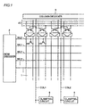
- Fig. 31 is a block diagram showing an example of a configuration of a dynamic random access memory (referred to as a "DRAM” hereinafter), a conventional semiconductor memory device.
- DRAM dynamic random access memory
- the semiconductor memory device is provided with subarrays 1 into which a memory cell array is divided, a row decoder 2 arranged at each subarray 1 for selecting a word line WL, and a column decoder 3 arranged at each subarray 1 for selecting a column select line CSL.
- the semiconductor memory device shown in Fig. 31 is a DRAM of x4 configuration and has a memory cell array consisting of four subarrays 1.
- Each subarray 1 has a plurality of word lines WL including a redundant word line, a plurality of pairs of bit lines arranged to cross the plurality of word lines WL and including a redundant pair of bit lines, and a plurality of column select lines CSL arranged parallel to the plurality of pairs of bit lines and including a redundant column select line for sending a signal for selecting a pair of bit lines.
- Cross points of word lines WL and the pairs of bit lines are connected to their respective memory cells (not shown) and thus the memory cells are arranged in a matrix.
- column select line CSL One end of column select line CSL is connected to column decoder 3 and the other end is opened.
- column select line CSL is disconnected due to foreign matters or the like, a redundant column select line is substituted for the column select line CSL while the disconnected portion is floating, causing multiselection of memory cells and hence malfunction of the device.
- a word line WLn also has one end connected to row decoder 2 while the other end open.
- a redundant word line is substituted for the disconnected word line WLn while the disconnected portion is floating, causing multiselection of memory cells and hence malfunction of the device.
- An object of the present invention is to clamp a column select line or a word line when the column select line or the word line is disconnected due to foreign matters or the like, so that the disconnected portion may not be floating.
- a semiconductor memory device includes a plurality of column select lines, a plurality of word lines, a memory cell array including a plurality of memory cells, a row decoder for selecting a word line, a column decoder for selecting a column select line, and a clamping circuit for fixing a column select line at a constant potential when the column decoder is inactivated.
- a semiconductor memory device includes a plurality of column select lines, a plurality of word lines, a memory cell array having a plurality of memory cells, a row decoder for selecting a word line, a column decoder for selecting a column select line, and a clamping circuit for fixing the word lines at a constant potential when the row decoder is inactivated.
- a semiconductor memory device includes a plurality of first signal lines, a plurality of memory cells connected to a first signal line, a decoder selectively activating the plurality of first signal lines, a plurality of second signal lines, a plurality of redundant memory cells connected to a second signal line, a replacement circuit for replacing a first signal line with a second signal line, and a clamp circuit for fixing a first signal line replaced with a second signal line at a constant potential.
- a main advantage of the present invention is that even when a column select line or a word line is disconnected due to foreign matters or the like, a malfunction where multiselection of memory cells is caused due to the floating, disconnected portion of the column select line or the word line can be prevented.
- Another advantage of the present invention lies in the capability to clamp an original signal line replaced with a redundant signal line.
- Fig. 1 shows the configuration of a semiconductor memory device according to a first embodiment of the present invention.
- Fig. 2 also shows a specific configuration thereof.
- Figs. 1 and 2 do not show a redundant circuit including a redundant word line, a redundant column select line and a redundant pair of bit lines.
- column decoder 3 is the same as that in the conventional semiconductor memory device described above and a description thereof will not be repeated here.
- Fig. 1 also shows an embodiment in which clamping circuits 8 are arranged each at one end of respective column select lines CSL1 and CSL2.
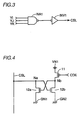
- Fig. 3 is a circuit diagram of an example of column decoder 3. Predecoded signals YI, YJ and YK produced from an address is input to an NAND circuit NA1, and an inverter INV1 outputs a column select signal.
- Fig. 4 is a circuit diagram of clamping circuit 8. As shown in Fig. 4, the clamping circuit includes a p channel MOS transistor (simply referred to as a p channel transistor hereinafter) 11 and n channel MOS transistors (simply referred to as n channel transistors hereinafter) 12a, 12b.
- a p channel MOS transistor (simply referred to as a p channel transistor hereinafter) 11
- n channel MOS transistors simply referred to as n channel transistors hereinafter) 12a, 12b.
- Figs. 5A-5G are waveform diagrams illustrating data read operation when column select line CSL1 for subarray 1 is disconnected.
- column decoder enable signal CDE is at inactive L level, so that p channel transistor 11 is turned on to set node Nb to H level, and node Na is clamped at L level.
- column decoder enable signal CDE is set to active H level and p channel transistor 11 is turned off.
- a word line WL2 selected by row decoder 2 is activated and transfer gates for memory cells 521-524 connected to word line WL2 are turned on, so that data written in each of the memory cells is read out on one of the paired bit lines. Then, as shown in Fig.
- sense amplifiers 41-44 are activated whereby a potential difference, for example, between paired bit lines B3 and B3 and as shown in Fig. 5E is sensed and the data read operation is thus completed.
- clamping circuit 8 clamps a disconnected portion CSL10 of column select line CSL1 shown in Fig. 2 at L level as shown in Fig. 5F, transfer gates 61a, 61b, 62a, 62b are turned off so that neither fluctuations of potential of an I/O line nor multiselection of memory cells, which would be caused in conventional circuits, is caused.
- column select line CSL2 When column decoder enable signal CDE is activated and column select line CSL2 is selected, column select line CSL2 is set to H level, as shown in Fig. 5F and transfer gates 63a, 63b, 73a, 73b, 64a, 64b, 74a, 74b are turned on, so that pairs of bit lines B3 and B3 , B4 and B4 , B30 and B30 , B40 and B40 are connected to an I/O line, and data written in the memory cells are accurately read out via the I/O line to a data bus.
- the column decoder shown in Fig. 3 functions to decode predecoded signals YI, YJ, YK into a signal having L level potential or a signal having H level potential and serves to clamp a non-selected column select line CSL at L level potential. Accordingly, in a semiconductor memory device according to the first embodiment, column select lines CSL1 and CSL2 both have respective clamping circuits, each at one end.
- clamping circuit 8 is provided opposite to column decoder 3 at one end of column select line CSLn, it is ensured that column select line CSL1 or CSL2 is clamped at L level. Thus, even when column select line CSL1 or CSL2 is disconnected, the disconnected portion will not float.
- clamping circuit 8 is disposed opposite to column decoder 3
- a plurality of clamp circuits 8 may be disposed at any portions, and the same applies to the following second, third, fourth and seventh embodiments.
- Fig. 6 is a block diagram of the configuration of a semiconductor memory device according a second embodiment of the present invention.
- a half-latch circuit 13 is provided opposite to column decoder 3 for column select line CSL to fix column select line CSL at L level.
- Fig. 7 is a circuit diagram of an exemplary specific configuration of the half-latch circuit shown in Fig. 6.
- the half-latch circuit includes an inverter INV2 and an n channel transistor 14.
- the output of inverter INV2 is set to H level and n channel transistor 14 is turned on so that the potential of node d is maintained at the L level.
- column select line CSL is fixed at L level (i.e., GND level). Therefore, the semiconductor memory device according to the second embodiment achieves a similar effect to that of a semiconductor memory device according to the first embodiment.
- Fig. 8 is a block diagram of the configuration of a semiconductor memory device according to a third embodiment of the present invention.
- an N channel transistor 15 receiving a power on reset signal POR at its gate is also provided between column select line CSL and half-latch circuit 13 in the semiconductor memory device according to the second embodiment.
- Fig. 9 is a circuit diagram of a power on reset circuit for generating the power on reset signal.
- the power on reset circuit includes an integration circuit 17 configured by a resistance R1 and a capacitor C1, and an inverter INV3 receiving an output of integration circuit 17.
- Fig. 10 is a timing chart illustrating the operation of the power on reset circuit.
- Vdd Ext.Vcc
- H power supply potential
- L level i.e., GND level
- the potential of node P in Fig. 8 is set to L level so that the output of inverter INV2 of half-latch circuit 13 shown in Fig. 7 is set to H level.
- n channel transistor 14 is turned on and the potential of node P is maintained at the L level.
- Fig. 11 shows the configuration of a semiconductor memory device according to a fourth embodiment of the present invention.
- a high resistance R2 is connected, opposite to column decoder 3, to one end of column select line CSL, to clamp column select line CSL at L level.
- the magnitude of high resistance R2 is adapted to be large enough to normally activate column select line CSL.
- the semiconductor memory device according to the fourth embodiment also achieves a similar effect to that of the semiconductor memory device according to the first embodiment.
- Fig. 12 shows the configuration of a semiconductor memory device according to a fifth embodiment of the present invention.
- the semiconductor memory device is provided with an n channel transistor 18 receiving a signal CDE at its gate, and a high resistance R3 connected to the source of n channel transistor 18 for preventing current from flowing through a selected column select line CSL when column decoder enable signal CDE is at active H level.
- Fig. 13 is a block diagram of a semiconductor memory device according to a sixth embodiment of the present invention.
- a column decoder 3a is provided at one end and a column decoder 3b is provided at the other end of column select line CSL.
- the semiconductor memory device according to the sixth embodiment achieves a similar effect to that of the first embodiment.
- Fig. 14 shows a semiconductor memory device according to a seventh embodiment of the present invention.
- an n channel transistor 19 receiving a signal V ⁇ at its gate is provided, opposite to column decoder 3, at one end of column select line CSL to clamp column select line CSL at L level via a high resistance.
- n channel transistor 19 Since the size of n channel transistor 19 is adapted to be sufficiently smaller than that of a transistor for driving column select line CSL (not shown), column select line CSL is normally activated.
- the signal V ⁇ always supplied to the gate of n channel transistor 19 is adapted to set to a level at which n channel transistor 19 slightly turns on or to be half the magnitude of a power supply voltage.
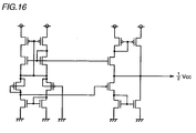
- the signal V ⁇ having a level at which n channel transistor 19 slightly turns on is generated by the circuit shown in Fig. 15, and the signal V ⁇ having half the magnitude of the power supply voltage is generated by the circuit shown in Fig. 16.
- the semiconductor memory device according to the seventh embodiment also achieves a similar effect to that of a semiconductor memory device according to the first embodiment.
- clamping circuit 8 is disposed opposite to column decoder 3, while such an arrangement is preferable.
- the number of clamping circuits is not limited, either.
- Fig. 17 shows the configuration of a semiconductor memory device according to an eighth embodiment of the present invention.
- a clamping circuit 22 is provided at a word line WLn at an end opposite to a row decoder 2.
- Fig. 18 is a circuit diagram showing one example of row decoder 2.
- X I , X J and X K represent predecoded signals produced from an address.
- RXn represents a select signal produced from the address for selecting one word line WL.
- the row decoder shown in Fig. 18 decodes addresses into either L level potential or H level potential and clamps a non-selected word line WL at L level potential.
- Fig. 19 is a circuit diagram showing a specific configuration of clamping circuit 22 shown in Fig. 17.
- a p channel transistor 23 turns on and the potential of a node Nb1 is set to H level, and an n channel transistor 24a turns on. Accordingly, the potential of a node Na1 is set to L level.
- p channel transistor 23 turns off, so that the potential of node Na1 is held at L level and word line WLn is clamped at L level.
- the both ends of word line WLn are clamped by row decoder 2 and clamping circuit 22.
- clamping circuit 22 is desirably provided at word line WLn at an end opposite to row decoder 2, the present embodiment is not limited to this and clamping circuits may be provided at any portions. This applies to the ninth to eleventh and thirteenth embodiments described hereinafter.
- Fig. 20 shows the configuration of a semiconductor memory device according to a ninth embodiment. As shown in Fig. 20, a half latch circuit 25 is provided at word line WLn opposite to row decoder 2 and clamps word line WLn at L level.
- Fig. 21 is a circuit diagram showing the configuration of half latch circuit 25 shown in Fig. 20.
- Half latch circuit 25 shown in Fig. 21 includes an inverter ILV5 and an n channel transistor 26, and when the potential of a node Nd1 is set to L level, the output of inverter INV5 is set to H level and n channel transistor 26 turns on so that the potential of node Nd1 is held at the L level.
- word line WLn is fixed at L level (GHD level).
- the semiconductor memory device according to the present embodiment has a similar effect to that of the semiconductor memory device according to the eighth embodiment.
- Fig. 22 shows the configuration of a semiconductor memory device according to a tenth embodiment.
- Half latch circuit 25 shown in Fig. 22 is the same as that shown in Fig.20.
- word line WL Since an n channel transistor 27 which receives at its gate the power on reset signal POR output from the power on reset circuit shown in Fig. 9 is provided at word line WL at the end opposite to row decoder 2, word line WL is ensured of being clamped at L level at the time of power-on.
- the operation of the power-on reset circuit is the same as that described in the third embodiment.
- the configuration of half latch circuit 25 is the same as that shown in Fig. 21.
- n channel transistor 27 since n channel transistor 27 turns on by inputting of a high level power on reset signal POR to the gate at the time of power-on, the potential of a node NP1 (Nd1) is set to L level. Accordingly the output of inverter INV5 shown in Fig. 21 is set to H level and n channel transistor 26 turns on so that the potential of node NP1 is held at L level.
- word line WL is ensured of being clamped at L level at the time of power-on.
- Fig. 23 shows the configuration of a semiconductor memory device according to an eleventh embodiment of the present invention.
- a high resistance R4 having one end grounded is connected to word line WL at the end opposite to row decoder 2 to clamp word line WL at L level.
- the magnitude of high resistance R4 is adapted to be large enough to normally activate word line WL.
- Fig. 24 shows the configuration of a semiconductor memory device according to a twelfth embodiment.
- row decoders 2 are provided at the both ends of word line WL and clamping function of row decoders 2 is employed to clamp word line WL.
- Fig. 25 shows the configuration of a semiconductor memory device according to a thirteenth embodiment of the present invention.
- an n channel transistor 37 which always receives a signal V R at its gate is provided at word line WLn at an end opposite to row decoder 2, to clamp word line WLn at L level by high resistance.
- the potential of the signal V R is adapted to be at a level at which n channel transistor 37 slightly turns on or to be half the magnitude of the power supply voltage.
- n channel transistor 37 is adapted to be sufficiently smaller than that of a transistor (not shown) which drives word line WLn.
- the signal V R of the level at which n channel transistor 37 slight turns on is generated by the circuit shown in Fig. 15, as with the signal V ⁇ .
- the signal V R having half the magnitude of the power supply voltage is generated by the circuit shown in Fig. 16, as with the signal V ⁇ .
- n channel transistors 37 for clamping word lines WL are provided to word line WL one for each, not all of the n channel transistors 37 are shown in Fig. 25.
- Fig. 26 shows a configuration of a semiconductor memory device according to a fourteenth embodiment of the present invention.
- the semiconductor memory device includes a memory cell array 40, a decoder 41, a signal line 42 such as a column select line and a word line selected by decoder 41, an n channel transistor 44 arranged at an end of signal line 42 opposite to decoder 41 and connected between signal line 42 and a ground node, a voltage set circuit 45 connected to the gate of n channel transistor 44 and outputting a signal b, a redundant memory cell array 55, a redundant decoder 56, a redundant signal line 57, and a program circuit 60.
- Fig. 27 is a circuit diagram showing one example of voltage set circuit 45 shown in Fig. 26.
- voltage set circuit 45 includes a fuse 46 grounded at its one end and a resistance 47 connected between fuse 46 and a power supply node. When fuse 46 is disconnected, voltage set circuit 45 outputs a signal b of high level via resistance 47.
- Fig. 28 is a circuit diagram showing another example of voltage set circuit 45 shown in Fig. 26.
- voltage set circuit 45 includes fuse 46 grounded at its one end and an n channel transistor 48 connected between fuse 46 and a power supply node and receiving a signal c at its gate.
- Signal c is a clock signal having such a voltage that n channel transistor 48 is slightly turned on or attaining high level only when decoder 41 is activated. When fuse 46 is disconnected, n channel transistor 48 is turned on and a signal b of high level is output.
- Fig. 29 is a circuit diagram showing still another example of voltage set circuit 45 shown in Fig. 26.
- voltage set circuit 45 includes fuse 46 grounded at its one end, a p channel transistor 50 connected between fuse 46 and a power supply node, an inverter 51 having an output terminal connected to the gate of p channel transistor 50 and having an input terminal connected to a node N1, and an n channel transistor 52 connected between the power supply node and node N1 and receiving a signal d at its gate.
- signal line 42 is fixed at low level so that there is no portion of floating level and thus malfunction is not caused.
- Fig. 30 shows a configuration of a semiconductor memory device according to fifteenth embodiment of the present invention.
- the semiconductor memory device is similar in configuration to the semiconductor memory device according to the fourteenth embodiment except for a fuse 54 arranged at an end of signal line 42 opposite to decoder 41 and grounded at its one end.
- the fuses (not shown) for signal lines which are not replaced with redundant signal line 57 are all disconnected so that fuse 54 for the replaced signal line 42 is not disconnected.
- signal line 42 is fixed at low level so that there is no portion of floating level and thus malfunction is not caused.
Abstract
Description
- The present invention relates to a semiconductor memory device. It particularly relates to a semiconductor memory device provided with a clamping circuit which prevents malfunction when a column select line or a word line is disconnected by foreign matters or the like.
- Fig. 31 is a block diagram showing an example of a configuration of a dynamic random access memory (referred to as a "DRAM" hereinafter), a conventional semiconductor memory device.
- As shown in Fig. 31, the semiconductor memory device is provided with
subarrays 1 into which a memory cell array is divided, arow decoder 2 arranged at eachsubarray 1 for selecting a word line WL, and acolumn decoder 3 arranged at eachsubarray 1 for selecting a column select line CSL. - Furthermore, the semiconductor memory device shown in Fig. 31 is a DRAM of x4 configuration and has a memory cell array consisting of four
subarrays 1. Eachsubarray 1 has a plurality of word lines WL including a redundant word line, a plurality of pairs of bit lines arranged to cross the plurality of word lines WL and including a redundant pair of bit lines, and a plurality of column select lines CSL arranged parallel to the plurality of pairs of bit lines and including a redundant column select line for sending a signal for selecting a pair of bit lines. Cross points of word lines WL and the pairs of bit lines are connected to their respective memory cells (not shown) and thus the memory cells are arranged in a matrix. - One end of column select line CSL is connected to
column decoder 3 and the other end is opened. Thus, when column select line CSL is disconnected due to foreign matters or the like, a redundant column select line is substituted for the column select line CSL while the disconnected portion is floating, causing multiselection of memory cells and hence malfunction of the device. - Furthermore, a word line WLn also has one end connected to
row decoder 2 while the other end open. Thus, when word line WLn is disconnected due to foreign matters or the like, a redundant word line is substituted for the disconnected word line WLn while the disconnected portion is floating, causing multiselection of memory cells and hence malfunction of the device. - An object of the present invention is to clamp a column select line or a word line when the column select line or the word line is disconnected due to foreign matters or the like, so that the disconnected portion may not be floating.
- A semiconductor memory device according to one aspect of the present invention includes a plurality of column select lines, a plurality of word lines, a memory cell array including a plurality of memory cells, a row decoder for selecting a word line, a column decoder for selecting a column select line, and a clamping circuit for fixing a column select line at a constant potential when the column decoder is inactivated.
- A semiconductor memory device according to another aspect of the present invention includes a plurality of column select lines, a plurality of word lines, a memory cell array having a plurality of memory cells, a row decoder for selecting a word line, a column decoder for selecting a column select line, and a clamping circuit for fixing the word lines at a constant potential when the row decoder is inactivated.
- A semiconductor memory device according to still another aspect of the present invention includes a plurality of first signal lines, a plurality of memory cells connected to a first signal line, a decoder selectively activating the plurality of first signal lines, a plurality of second signal lines, a plurality of redundant memory cells connected to a second signal line, a replacement circuit for replacing a first signal line with a second signal line, and a clamp circuit for fixing a first signal line replaced with a second signal line at a constant potential.
- Accordingly, a main advantage of the present invention is that even when a column select line or a word line is disconnected due to foreign matters or the like, a malfunction where multiselection of memory cells is caused due to the floating, disconnected portion of the column select line or the word line can be prevented.
- Another advantage of the present invention lies in the capability to clamp an original signal line replaced with a redundant signal line.
- The foregoing and other objects, features, aspects and advantages of the present invention will become more apparent from the following detailed description of the present invention when taken in conjunction with the accompanying drawings.
-
- Fig. 1 shows the configuration of a semiconductor memory device according to a first embodiment of the present invention.
- Fig. 2 specifically shows the configuration of the semiconductor memory device shown in Fig. 1.
- Fig. 3 is a circuit diagram of the column decoder shown in Fig. 2.
- Fig. 4 is a specific circuit diagram of the configuration of the clamping circuit shown in Fig. 2.
- Figs. 5A-5G are timing charts illustrating data read operation when a column select line for a subarray shown in Fig. 1 is disconnected.
- Fig. 6 shows the configuration of a semiconductor memory device according to a second embodiment of the present invention.
- Fig. 7 is a circuit diagram illustrating a specific configuration of the half-latch circuit shown in Fig. 6.
- Fig. 8 shows the configuration of a semiconductor memory device according to a third embodiment of the present invention.
- Fig. 9 is a circuit diagram illustrating a specific configuration of a power on reset circuit for generating power on reset signals shown in Fig. 8.
- Fig. 10 is a timing chart illustrating operation of the power on reset circuit shown in Fig. 9.
- Fig. 11 shows the configuration of a semiconductor memory device according to a fourth embodiment of the present invention.
- Fig. 12 shows the configuration of a semiconductor memory device according to a fifth embodiment of the present invention.
- Fig. 13 shows the configuration of a semiconductor memory device according to a sixth embodiment of the present invention.
- Fig. 14 shows the configuration of a semiconductor memory device according to a seventh embodiment of the present invention.
- Fig. 15 is a circuit diagram showing a circuit which generates the signal V for slightly turning on the n channel transistor shown in Fig. 14.
- Fig. 16 is a circuit diagram showing a circuit for generating a signal V when the magnitude of the signal V is half that of that of a power supply voltage.
- Fig. 17 is a block diagram showing the configuration of a semiconductor memory device according to an eighth embodiment of the present invention.
- Fig. 18 is a circuit diagram showing one example of the configuration of the row decoder shown in Fig. 17.
- Fig. 19 is a circuit diagram showing the configuration of the clamping circuit shown in Fig. 17.
- Fig. 20 is a block diagram showing the configuration of a semiconductor memory device according to a ninth embodiment of the present invention.
- Fig. 21 is a circuit diagram showing the configuration of the half latch circuit shown in Fig. 20.
- Figs. 22-25 are block diagrams showing the configurations of semiconductor memory devices according to tenth to thirteenth embodiments of the present invention, respectively.
- Fig. 26 shows a configuration of a semiconductor memory device according to a fourteenth embodiment of the present invention.
- Fig. 27 is a circuit diagram showing one example of the configuration of the voltage set circuit shown in Fig. 26.
- Fig. 28 is a circuit diagram showing another example of the configuration of the voltage set circuit shown in Fig. 26.
- Fig. 29 is a circuit diagram showing still another example of the configuration of the voltage set circuit shown in Fig. 26.
- Fig. 30 shows a configuration of a semiconductor memory device according to a fifteenth embodiment of the present invention.
- Fig. 31 shows a configuration of a conventional semiconductor memory device.
-
- Fig. 1 shows the configuration of a semiconductor memory device according to a first embodiment of the present invention. Fig. 2 also shows a specific configuration thereof.
- Figs. 1 and 2 do not show a redundant circuit including a redundant word line, a redundant column select line and a redundant pair of bit lines.
- In Fig. 1,
column decoder 3 is the same as that in the conventional semiconductor memory device described above and a description thereof will not be repeated here. - As shown in Fig. 2, the semiconductor memory device according to the first embodiment also includes
sense amplifiers Bn (n=1, 2, 3, or 4), memory cells 511-514, 521-524 each arranged at a cross point of a word line WL and the pair of bit lines Bn,Bn (n=0, 1, 2, 3 or 4), transfer gates 61-64, 71-74 for selecting a pair of bit lines in response to a column select signal, and aclamping circuit 8 for clamping column select lines CSL1, CSL2. - Fig. 1 also shows an embodiment in which
clamping circuits 8 are arranged each at one end of respective column select lines CSL1 and CSL2. - Fig. 3 is a circuit diagram of an example of
column decoder 3. Predecoded signals YI, YJ and YK produced from an address is input to an NAND circuit NA1, and an inverter INV1 outputs a column select signal. - Fig. 4 is a circuit diagram of
clamping circuit 8. As shown in Fig. 4, the clamping circuit includes a p channel MOS transistor (simply referred to as a p channel transistor hereinafter) 11 and n channel MOS transistors (simply referred to as n channel transistors hereinafter) 12a, 12b. - Figs. 5A-5G are waveform diagrams illustrating data read operation when column select line CSL1 for
subarray 1 is disconnected. - The operation of a semiconductor memory device according to the first embodiment will now be described.
- In the clamping circuit shown in Fig. 4, when a column decoder enable signal CDE is at inactive L level,
p channel transistor 11 is turned on and the potential of a node Nb is set to H level. Then,n channel transistor 12a is turned on and the potential of a node Na is set to L level. When the column decoder enable signal CDE is set to active H level,p channel transistor 11 is turned off so that the potential of node Na is maintained at the L level and thus column select line CSL is clamped at L level. - Referring now to the waveform diagrams of Figs. 5A-5G, the operation of
subarray 1 shown in Fig. 2 will be described. - As shown in Fig. 5A, prior to data read operation (i.e., in a stand-by state), column decoder enable signal CDE is at inactive L level, so that
p channel transistor 11 is turned on to set node Nb to H level, and node Na is clamped at L level. When a data read operation is started, column decoder enable signal CDE is set to active H level andp channel transistor 11 is turned off. Furthermore, as shown in Fig. 5B, a word line WL2 selected byrow decoder 2 is activated and transfer gates for memory cells 521-524 connected to word line WL2 are turned on, so that data written in each of the memory cells is read out on one of the paired bit lines. Then, as shown in Fig. 5C , when the level of a sense amplifier driving signalSAN input to an n channel flipflop is changed from Vcc/2 to GND and a sense amplifier driving signal SAP input to a p channel flipflop is changed from Vcc/2 to Vcc, sense amplifiers 41-44 are activated whereby a potential difference, for example, between paired bit lines B3 andB3 and as shown in Fig. 5E is sensed and the data read operation is thus completed. - As clamping
circuit 8 clamps a disconnected portion CSL10 of column select line CSL1 shown in Fig. 2 at L level as shown in Fig. 5F,transfer gates - When column decoder enable signal CDE is activated and column select line CSL2 is selected, column select line CSL2 is set to H level, as shown in Fig. 5F and
transfer gates B3 , B4 andB4 , B30 andB30 , B40 andB40 are connected to an I/O line, and data written in the memory cells are accurately read out via the I/O line to a data bus. - The column decoder shown in Fig. 3 functions to decode predecoded signals YI, YJ, YK into a signal having L level potential or a signal having H level potential and serves to clamp a non-selected column select line CSL at L level potential. Accordingly, in a semiconductor memory device according to the first embodiment, column select lines CSL1 and CSL2 both have respective clamping circuits, each at one end.
- In the semiconductor memory device according to the first embodiment, as clamping
circuit 8 is provided opposite tocolumn decoder 3 at one end of column select line CSLn, it is ensured that column select line CSL1 or CSL2 is clamped at L level. Thus, even when column select line CSL1 or CSL2 is disconnected, the disconnected portion will not float. - While preferably clamping
circuit 8 is disposed opposite tocolumn decoder 3, a plurality ofclamp circuits 8 may be disposed at any portions, and the same applies to the following second, third, fourth and seventh embodiments. - Fig. 6 is a block diagram of the configuration of a semiconductor memory device according a second embodiment of the present invention.
- In the semiconductor memory device according to the second embodiment, as shown in Fig. 6, a half-
latch circuit 13 is provided opposite tocolumn decoder 3 for column select line CSL to fix column select line CSL at L level. - Fig. 7 is a circuit diagram of an exemplary specific configuration of the half-latch circuit shown in Fig. 6. The half-latch circuit includes an inverter INV2 and an
n channel transistor 14. When the potential of a node d is at L level, the output of inverter INV2 is set to H level andn channel transistor 14 is turned on so that the potential of node d is maintained at the L level. Thus, column select line CSL is fixed at L level (i.e., GND level). Therefore, the semiconductor memory device according to the second embodiment achieves a similar effect to that of a semiconductor memory device according to the first embodiment. - Fig. 8 is a block diagram of the configuration of a semiconductor memory device according to a third embodiment of the present invention. In the semiconductor memory device according to the third embodiment, as shown in Fig. 8, an
N channel transistor 15 receiving a power on reset signal POR at its gate is also provided between column select line CSL and half-latch circuit 13 in the semiconductor memory device according to the second embodiment. - Fig. 9 is a circuit diagram of a power on reset circuit for generating the power on reset signal. As shown in Fig. 9, the power on reset circuit includes an
integration circuit 17 configured by a resistance R1 and a capacitor C1, and an inverter INV3 receiving an output ofintegration circuit 17. - Fig. 10 is a timing chart illustrating the operation of the power on reset circuit. In the power on reset circuit, electric charges are stored in capacitor C1 via resistance R1 at power-on, resulting in the potential of a node Q shown in Fig. 9. When the potential of node Q is below a threshold voltage Vth, power on reset signal POR is at a power supply potential Vdd (= Ext.Vcc) or H level. When the potential of node Q reaches or exceeds the threshold voltage, power on reset signal POR is set to L level (i.e., GND level). Thus, since
n channel transistor 15 is turned on at the time of power-on, the potential of node P is set to L level. Thus, the potential of node P in Fig. 8 is set to L level so that the output of inverter INV2 of half-latch circuit 13 shown in Fig. 7 is set to H level. Then,n channel transistor 14 is turned on and the potential of node P is maintained at the L level. - Thus, in the semiconductor memory device according to the third embodiment, it is ensured that column line CSL is clamped at L level at the time of power-on.
- Fig. 11 shows the configuration of a semiconductor memory device according to a fourth embodiment of the present invention.
- In the semiconductor memory device, as shown in Fig. 11, a high resistance R2 is connected, opposite to
column decoder 3, to one end of column select line CSL, to clamp column select line CSL at L level. - The magnitude of high resistance R2 is adapted to be large enough to normally activate column select line CSL.
- The semiconductor memory device according to the fourth embodiment also achieves a similar effect to that of the semiconductor memory device according to the first embodiment.
- Fig. 12 shows the configuration of a semiconductor memory device according to a fifth embodiment of the present invention.
- As shown in Fig. 12, the semiconductor memory device is provided with an
n channel transistor 18 receiving a signalCDE at its gate, and a high resistance R3 connected to the source ofn channel transistor 18 for preventing current from flowing through a selected column select line CSL when column decoder enable signal CDE is at active H level. - Combination of the fifth embodiment and any of the other embodiments further enhances reliability of column select line CSL.
- Fig. 13 is a block diagram of a semiconductor memory device according to a sixth embodiment of the present invention.
- In the semiconductor memory device, as shown in Fig. 13, a
column decoder 3a is provided at one end and acolumn decoder 3b is provided at the other end of column select line CSL. - As described in the first embodiment, since
column decoders - Fig. 14 shows a semiconductor memory device according to a seventh embodiment of the present invention. As shown in Fig. 14, in the semiconductor memory device, an
n channel transistor 19 receiving a signal V at its gate is provided, opposite tocolumn decoder 3, at one end of column select line CSL to clamp column select line CSL at L level via a high resistance. - Since the size of
n channel transistor 19 is adapted to be sufficiently smaller than that of a transistor for driving column select line CSL (not shown), column select line CSL is normally activated. - Furthermore, the signal V always supplied to the gate of
n channel transistor 19 is adapted to set to a level at whichn channel transistor 19 slightly turns on or to be half the magnitude of a power supply voltage. - Specifically, the signal V having a level at which
n channel transistor 19 slightly turns on is generated by the circuit shown in Fig. 15, and the signal V having half the magnitude of the power supply voltage is generated by the circuit shown in Fig. 16. - The semiconductor memory device according to the seventh embodiment also achieves a similar effect to that of a semiconductor memory device according to the first embodiment.
- All of the above embodiments are not limited to an arrangement in which
clamping circuit 8 is disposed opposite tocolumn decoder 3, while such an arrangement is preferable. The number of clamping circuits is not limited, either. - Fig. 17 shows the configuration of a semiconductor memory device according to an eighth embodiment of the present invention.
- In the semiconductor memory device according to the eighth embodiment, as shown in Fig. 17, a clamping
circuit 22 is provided at a word line WLn at an end opposite to arow decoder 2. - Fig. 18 is a circuit diagram showing one example of
row decoder 2. In Fig. 18, XI, XJ and XK represent predecoded signals produced from an address. RXn represents a select signal produced from the address for selecting one word line WL. - The row decoder shown in Fig. 18 decodes addresses into either L level potential or H level potential and clamps a non-selected word line WL at L level potential.
- Fig. 19 is a circuit diagram showing a specific configuration of clamping
circuit 22 shown in Fig. 17. - In the clamping circuit shown in Fig. 19, for a period during which the row address control signal RAS is inactivated (that is, a period during which
RAS is at H level),a p channel transistor 23 turns on and the potential of a node Nb1 is set to H level, and ann channel transistor 24a turns on. Accordingly, the potential of a node Na1 is set to L level. When the row address control signal RAS is set to an active H level,p channel transistor 23 turns off, so that the potential of node Na1 is held at L level and word line WLn is clamped at L level. - In the semiconductor memory device according to the eighth embodiment, the both ends of word line WLn are clamped by
row decoder 2 and clampingcircuit 22. - Thus, according to this semiconductor memory device, even when word line WLn is disconnected, the disconnected portion does not float.
- Although clamping
circuit 22 is desirably provided at word line WLn at an end opposite to rowdecoder 2, the present embodiment is not limited to this and clamping circuits may be provided at any portions. This applies to the ninth to eleventh and thirteenth embodiments described hereinafter. - Fig. 20 shows the configuration of a semiconductor memory device according to a ninth embodiment. As shown in Fig. 20, a
half latch circuit 25 is provided at word line WLn opposite to rowdecoder 2 and clamps word line WLn at L level. - Fig. 21 is a circuit diagram showing the configuration of
half latch circuit 25 shown in Fig. 20. -
Half latch circuit 25 shown in Fig. 21 includes an inverter ILV5 and ann channel transistor 26, and when the potential of a node Nd1 is set to L level, the output of inverter INV5 is set to H level andn channel transistor 26 turns on so that the potential of node Nd1 is held at the L level. - Thus, word line WLn is fixed at L level (GHD level).
- Thus, the semiconductor memory device according to the present embodiment has a similar effect to that of the semiconductor memory device according to the eighth embodiment.
- Fig. 22 shows the configuration of a semiconductor memory device according to a tenth embodiment.
Half latch circuit 25 shown in Fig. 22 is the same as that shown in Fig.20. - Since an
n channel transistor 27 which receives at its gate the power on reset signal POR output from the power on reset circuit shown in Fig. 9 is provided at word line WL at the end opposite to rowdecoder 2, word line WL is ensured of being clamped at L level at the time of power-on. - The operation of the power-on reset circuit is the same as that described in the third embodiment. The configuration of
half latch circuit 25 is the same as that shown in Fig. 21. - In Fig. 22, since
n channel transistor 27 turns on by inputting of a high level power on reset signal POR to the gate at the time of power-on, the potential of a node NP1 (Nd1) is set to L level. Accordingly the output of inverter INV5 shown in Fig. 21 is set to H level andn channel transistor 26 turns on so that the potential of node NP1 is held at L level. - Thus, word line WL is ensured of being clamped at L level at the time of power-on.
- Fig. 23 shows the configuration of a semiconductor memory device according to an eleventh embodiment of the present invention.
- As shown in Fig. 23, in the semiconductor memory device according to the present embodiment, a high resistance R4 having one end grounded is connected to word line WL at the end opposite to row
decoder 2 to clamp word line WL at L level. - The magnitude of high resistance R4 is adapted to be large enough to normally activate word line WL.
- Fig. 24 shows the configuration of a semiconductor memory device according to a twelfth embodiment.
- As shown in Fig. 24, in the semiconductor memory device according to the present embodiment,
row decoders 2 are provided at the both ends of word line WL and clamping function ofrow decoders 2 is employed to clamp word line WL. - Fig. 25 shows the configuration of a semiconductor memory device according to a thirteenth embodiment of the present invention.
- As shown in Fig. 25, in the semiconductor memory device according to the present embodiment, an
n channel transistor 37 which always receives a signal VR at its gate is provided at word line WLn at an end opposite to rowdecoder 2, to clamp word line WLn at L level by high resistance. The potential of the signal VR is adapted to be at a level at whichn channel transistor 37 slightly turns on or to be half the magnitude of the power supply voltage. - The size of
n channel transistor 37 is adapted to be sufficiently smaller than that of a transistor (not shown) which drives word line WLn. The signal VR of the level at whichn channel transistor 37 slight turns on is generated by the circuit shown in Fig. 15, as with the signal V. The signal VR having half the magnitude of the power supply voltage is generated by the circuit shown in Fig. 16, as with the signal V. - Although in the present embodiment also,
n channel transistors 37 for clamping word lines WL are provided to word line WL one for each, not all of then channel transistors 37 are shown in Fig. 25. - Fig. 26 shows a configuration of a semiconductor memory device according to a fourteenth embodiment of the present invention. As shown in the figure, the semiconductor memory device includes a
memory cell array 40, adecoder 41, asignal line 42 such as a column select line and a word line selected bydecoder 41, ann channel transistor 44 arranged at an end ofsignal line 42 opposite todecoder 41 and connected betweensignal line 42 and a ground node, avoltage set circuit 45 connected to the gate ofn channel transistor 44 and outputting a signal b, a redundantmemory cell array 55, aredundant decoder 56, aredundant signal line 57, and aprogram circuit 60. - Fig. 27 is a circuit diagram showing one example of voltage set
circuit 45 shown in Fig. 26. As shown in Fig. 27, voltage setcircuit 45 includes afuse 46 grounded at its one end and aresistance 47 connected betweenfuse 46 and a power supply node. Whenfuse 46 is disconnected, voltage setcircuit 45 outputs a signal b of high level viaresistance 47. - Fig. 28 is a circuit diagram showing another example of voltage set
circuit 45 shown in Fig. 26. As shown in Fig. 28, voltage setcircuit 45 includesfuse 46 grounded at its one end and ann channel transistor 48 connected betweenfuse 46 and a power supply node and receiving a signal c at its gate. - Signal c is a clock signal having such a voltage that
n channel transistor 48 is slightly turned on or attaining high level only whendecoder 41 is activated. Whenfuse 46 is disconnected,n channel transistor 48 is turned on and a signal b of high level is output. - Fig. 29 is a circuit diagram showing still another example of voltage set
circuit 45 shown in Fig. 26. As shown in Fig. 29, voltage setcircuit 45 includesfuse 46 grounded at its one end,a p channel transistor 50 connected betweenfuse 46 and a power supply node, aninverter 51 having an output terminal connected to the gate ofp channel transistor 50 and having an input terminal connected to a node N1, and ann channel transistor 52 connected between the power supply node and node N1 and receiving a signal d at its gate. - When a pulse signal which attains high level only at the time of power-on is supplied to the gate of
n channel transistor 52 as signal d, fuse 46 is disconnected and a signal b of high level is output from node N1. - An operation by which signal
line 42 is replaced withredundant signal line 57 will now be described. - When an address which selects
signal line 42 is input toprogram circuit 60, a disenable signalDE inactivating decoder 41 is supplied todecoder 41 and an enable signal E activatingredundant decoder 56 is also supplied toredundant decoder 56 and thusredundant signal line 57 is selected. Whenfuse 46 included in voltage setcircuit 45 is disconnected, signal b output from voltage setcircuit 45 attains high level andn channel transistor 44 is turned on. This allowsonly signal line 42 replaced withredundant signal line 57 to be fixed at low level. - Thus, even if
signal line 42 replaced withredundant signal line 57 has been disconnected,signal line 42 is fixed at low level so that there is no portion of floating level and thus malfunction is not caused. - When
fuse 46 included in voltage setcircuit 45 is not disconnected, signal b attains low level and current flows to the ground node viafuse 46. However, the magnitude of the current is reduced depending on the magnitude ofresistance 47 or by supplying signals c and d to the gates ofn channel transistors - Fig. 30 shows a configuration of a semiconductor memory device according to fifteenth embodiment of the present invention. As shown in Fig. 30, the semiconductor memory device is similar in configuration to the semiconductor memory device according to the fourteenth embodiment except for a
fuse 54 arranged at an end ofsignal line 42 opposite todecoder 41 and grounded at its one end. - In a semiconductor memory device thus configured, the fuses (not shown) for signal lines which are not replaced with
redundant signal line 57 are all disconnected so thatfuse 54 for the replacedsignal line 42 is not disconnected. - Thus, even if
signal line 42 replaced withredundant signal line 57 has been disconnected,signal line 42 is fixed at low level so that there is no portion of floating level and thus malfunction is not caused. - Although the present invention has been described and illustrated in detail, it is clearly understood that the same is by way of illustration and example only and is not to be taken by way of limitation, the spirit and scope of the present invention being limited only by the terms of the appended claims.
Claims (11)
- A semiconductor memory device comprising:a plurality of column select lines (CSLn) arranged in columns;a plurality of word lines (WLn) arranged in rows;a memory cell array including a plurality of memory cells arranged in a matrix of the columns and rows;a row decoder (2) for selecting a word line among said plurality of word lines (WLn);a column decoder (3) for selecting a column select line among said plurality of column select lines (CSLn); andclamping means (8) for clamping said plurality of column select lines (CSLn) at a constant potential when said column decoder (3) is inactivated;
characterized in thatsaid clamping means (8) is controlled in response to a control signal (CDE) for activating said column decoder (3). - The semiconductor memory device according to claim 1, wherein said clamping means (8) fixes said plurality of column select lines (CSLn) at a ground potential.
- The semiconductor memory device according to one of claims 1 to 2, wherein said clamping means (8) is connected at an end of any of said plurality of column select lines (CSLn) opposite to said column decoder (3), preferably clamping means (22) being provided for clamping said plurality of word lines (WLn) at a constant potential when said row decoder (2) is inactivated.
- A semiconductor memory device comprising:a plurality of column select lines (CSLn) arranged in columns;a plurality of word lines (WLn) arranged in rows;a memory cell array including a plurality of memory cells arranged in a matrix of the columns and rows;a row decoder (2) for selecting a word line among said plurality of word lines (WLn); anda column decoder (3) for selecting a column select line among said plurality of column select lines (CSLn);
characterized by:a plurality of clamping means (22) corresponding to said plurality of word lines (WLn), each connected to an end of the corresponding word line, and for clamping the corresponding word line at a constant potential according to a potential at the end of the corresponding word line when said row decoder (2) is inactivated. - The semiconductor memory device according to claim 4, wherein each of said plurality of clamping means (22) includes:a first ground node (GN10);a second ground node (GN12);a power supply node (VN2);a first n channel transistor (24a) having its source connected to said first ground node (GN10) and having its drain connected to any one of said plurality of word lines (WLn);a second n channel transistor (24b) having its gate connected to said first n channel transistor (24a) at its drain, its source connected to said second ground node (GN12), and its drain connected to said first n channel transistor (24a) at its gate; anda p channel transistor (23) having its source connected to said power supply node (VN2) and its drain connected to said second n channel transistor (24b), being supplied at its gate with a row address control signal activated at high level.
- The semiconductor memory device according to claim 4 or 5, wherein each of said plurality of clamping means (22) fixes said plurality of word lines (WLn) at a ground potential.
- The semiconductor memory device according to one of claims 4 to 6, wherein each of said plurality of clamping means (22) is connected to one of said plurality of word lines (WLn) at the end opposite to said row decoder (2), preferably clamping means (8) being provided for clamping said plurality of column select lines (CSLn) at a constant potential when said column decoder (3) is inactivated.
- A semiconductor memory device comprising:a plurality of first signal lines (a);a plurality of memory cells connected to said first signal lines (a);a decoder (41) selectively activating said plurality of first signal lines (a);a plurality of second signal lines (57);a plurality of redundant memory cells connected to said second signal lines (57);replacing means (60) for replacing one of said first signal lines (a) with one of said second signal lines (57); anda plurality of clamping means (44, 45) for clamping any one of said first signal lines (a) replaced with the one of said second signal lines (57) at a constant potential, wherein each of said plurality of clamping means (44, 45) includesa ground node,a transistor (44) connected between the one of said first signal lines (a) and the ground node, and
characterized by:a voltage supply means (45) for supplying a voltage to a gate of said transistor (44). - The semiconductor memory device according to claim 8, wherein said voltage supply means (45) includessaid ground node, anda fuse (46) connected between the gate of said transistor (44) and the ground node.
- A semiconductor memory device comprising:a plurality of column select lines (CSL) arranged in columns;a column decoder (3) for selecting a column select line among said plurality of column select lines (CSL);a ground node (GN4); and
characterized by:a plurality of resistances (R2) connected between respective ends of said plurality of column select lines (CSL) and the ground node (GN4). - A semiconductor memory device comprising:a plurality of word lines (WLn) arranged in rows;a row decoder (2) for selecting a word line among said plurality of word lines (WLn);a ground node (GN16); and
characterized bya plurality of resistances (R4) connected between respective ends of said plurality of word lines (WLn) and the ground node (GN16).
Applications Claiming Priority (7)
| Application Number | Priority Date | Filing Date | Title |
|---|---|---|---|
| JP4525596 | 1996-03-01 | ||
| JP4525596 | 1996-03-01 | ||
| JP19820496 | 1996-07-26 | ||
| JP19820496 | 1996-07-26 | ||
| JP32195096 | 1996-12-02 | ||
| JP32195096 | 1996-12-02 | ||
| EP97103296A EP0797211A1 (en) | 1996-03-01 | 1997-02-27 | Semiconductor memory device with clamping circuit for preventing malfunction |
Related Parent Applications (2)
| Application Number | Title | Priority Date | Filing Date |
|---|---|---|---|
| EP97103296.6 Division | 1997-02-27 | ||
| EP97103296A Division EP0797211A1 (en) | 1996-03-01 | 1997-02-27 | Semiconductor memory device with clamping circuit for preventing malfunction |
Publications (2)
| Publication Number | Publication Date |
|---|---|
| EP0953983A2 true EP0953983A2 (en) | 1999-11-03 |
| EP0953983A3 EP0953983A3 (en) | 2005-10-05 |
Family
ID=27292165
Family Applications (2)
| Application Number | Title | Priority Date | Filing Date |
|---|---|---|---|
| EP97103296A Ceased EP0797211A1 (en) | 1996-03-01 | 1997-02-27 | Semiconductor memory device with clamping circuit for preventing malfunction |
| EP99113847A Withdrawn EP0953983A3 (en) | 1996-03-01 | 1997-02-27 | Semiconductor memory device with clamping circuit for preventing malfunction |
Family Applications Before (1)
| Application Number | Title | Priority Date | Filing Date |
|---|---|---|---|
| EP97103296A Ceased EP0797211A1 (en) | 1996-03-01 | 1997-02-27 | Semiconductor memory device with clamping circuit for preventing malfunction |
Country Status (4)
| Country | Link |
|---|---|
| US (1) | US5835419A (en) |
| EP (2) | EP0797211A1 (en) |
| KR (1) | KR100283022B1 (en) |
| CN (3) | CN101042928A (en) |
Cited By (1)
| Publication number | Priority date | Publication date | Assignee | Title |
|---|---|---|---|---|
| US8735885B2 (en) | 2007-12-14 | 2014-05-27 | Semiconductor Energy Laboratory Co., Ltd. | Antifuse memory device |
Families Citing this family (7)
| Publication number | Priority date | Publication date | Assignee | Title |
|---|---|---|---|---|
| JP4084918B2 (en) * | 2000-11-06 | 2008-04-30 | 富士通株式会社 | Selection signal generation circuit, bus selection circuit, and semiconductor memory device |
| GB2390702B (en) * | 2002-04-22 | 2006-04-12 | Micron Technology Inc | Providing a register file memory with local addressing in a SIMD parallel processor |
| JP4504397B2 (en) | 2007-05-29 | 2010-07-14 | 株式会社東芝 | Semiconductor memory device |
| US7692975B2 (en) * | 2008-05-09 | 2010-04-06 | Micron Technology, Inc. | System and method for mitigating reverse bias leakage |
| US8902676B2 (en) * | 2012-04-26 | 2014-12-02 | SK Hynix Inc. | Wordline coupling reduction technique |
| US11521697B2 (en) | 2019-01-30 | 2022-12-06 | STMicroelectronics International, N.V. | Circuit and method for at speed detection of a word line fault condition in a memory circuit |
| US11393532B2 (en) | 2019-04-24 | 2022-07-19 | Stmicroelectronics International N.V. | Circuit and method for at speed detection of a word line fault condition in a memory circuit |
Citations (7)
| Publication number | Priority date | Publication date | Assignee | Title |
|---|---|---|---|---|
| FR2191202A1 (en) * | 1972-06-30 | 1974-02-01 | Ibm | |
| US4587638A (en) * | 1983-07-13 | 1986-05-06 | Micro-Computer Engineering Corporation | Semiconductor memory device |
| US4694432A (en) * | 1984-03-16 | 1987-09-15 | Mitsubishi Denki Kabushiki Kaisha | Semiconductor memory device |
| US4760559A (en) * | 1985-07-10 | 1988-07-26 | Mitsubishi Denki Kabushiki Kaisha | Semiconductor memory device |
| US5161121A (en) * | 1988-06-27 | 1992-11-03 | Oki Electric Industry Co., Ltd. | Random access memory including word line clamping circuits |
| US5363331A (en) * | 1991-12-24 | 1994-11-08 | Oki Electric Industry Co., Ltd. | Semiconductor memory with column line control circuits for protection against broken column lines |
| US5465233A (en) * | 1993-05-28 | 1995-11-07 | Sgs-Thomson Microelectronics, Inc. | Structure for deselecting broken select lines in memory arrays |
Family Cites Families (16)
| Publication number | Priority date | Publication date | Assignee | Title |
|---|---|---|---|---|
| JPS606040B2 (en) * | 1979-06-07 | 1985-02-15 | 日本電気株式会社 | integrated circuit |
| JPS58153294A (en) * | 1982-03-04 | 1983-09-12 | Mitsubishi Electric Corp | Semiconductor storage device |
| JPS5960794A (en) * | 1982-09-29 | 1984-04-06 | Fujitsu Ltd | Dynamic semiconductor storage device |
| JPS5979488A (en) * | 1982-10-28 | 1984-05-08 | Nec Corp | Mos memory circuit |
| JPS59116985A (en) * | 1982-11-29 | 1984-07-06 | Fujitsu Ltd | Semiconductor memory |
| JPS60206164A (en) * | 1984-03-30 | 1985-10-17 | Toshiba Corp | Semiconductor memory device |
| JPS6290950A (en) * | 1985-10-16 | 1987-04-25 | Mitsubishi Electric Corp | Semiconductor device |
| JPS63308386A (en) * | 1987-01-30 | 1988-12-15 | Sony Corp | Semiconductor device and manufacture thereof |
| US5204842A (en) * | 1987-08-05 | 1993-04-20 | Mitsubishi Denki Kabushiki Kaisha | Semiconductor memory with memory unit comprising a plurality of memory blocks |
| JPS6481250A (en) * | 1987-09-22 | 1989-03-27 | Nec Corp | Semiconductor memory device having multilayer metal wiring structure |
| JPH027286A (en) * | 1988-06-27 | 1990-01-11 | Oki Electric Ind Co Ltd | Dynamic ram |
| JPH0775118B2 (en) * | 1989-03-20 | 1995-08-09 | 三菱電機株式会社 | Semiconductor memory device |
| JPH0417197A (en) * | 1990-05-10 | 1992-01-21 | Mitsubishi Electric Corp | Semiconductor memory device |
| JP2617617B2 (en) * | 1990-11-16 | 1997-06-04 | 九州日本電気株式会社 | Semiconductor memory |
| JPH05210978A (en) * | 1992-01-31 | 1993-08-20 | Sharp Corp | Semiconductor memory |
| JP3354231B2 (en) * | 1993-09-29 | 2002-12-09 | 三菱電機エンジニアリング株式会社 | Semiconductor device |
-
1997
- 1997-02-27 EP EP97103296A patent/EP0797211A1/en not_active Ceased
- 1997-02-27 EP EP99113847A patent/EP0953983A3/en not_active Withdrawn
- 1997-02-27 US US08/807,742 patent/US5835419A/en not_active Expired - Lifetime
- 1997-02-28 KR KR1019970006857A patent/KR100283022B1/en not_active IP Right Cessation
- 1997-03-01 CN CNA2007100936079A patent/CN101042928A/en active Pending
- 1997-03-01 CN CNA200310119910A patent/CN1505047A/en active Pending
- 1997-03-01 CN CNB971109443A patent/CN1153220C/en not_active Expired - Lifetime
Patent Citations (7)
| Publication number | Priority date | Publication date | Assignee | Title |
|---|---|---|---|---|
| FR2191202A1 (en) * | 1972-06-30 | 1974-02-01 | Ibm | |
| US4587638A (en) * | 1983-07-13 | 1986-05-06 | Micro-Computer Engineering Corporation | Semiconductor memory device |
| US4694432A (en) * | 1984-03-16 | 1987-09-15 | Mitsubishi Denki Kabushiki Kaisha | Semiconductor memory device |
| US4760559A (en) * | 1985-07-10 | 1988-07-26 | Mitsubishi Denki Kabushiki Kaisha | Semiconductor memory device |
| US5161121A (en) * | 1988-06-27 | 1992-11-03 | Oki Electric Industry Co., Ltd. | Random access memory including word line clamping circuits |
| US5363331A (en) * | 1991-12-24 | 1994-11-08 | Oki Electric Industry Co., Ltd. | Semiconductor memory with column line control circuits for protection against broken column lines |
| US5465233A (en) * | 1993-05-28 | 1995-11-07 | Sgs-Thomson Microelectronics, Inc. | Structure for deselecting broken select lines in memory arrays |
Cited By (1)
| Publication number | Priority date | Publication date | Assignee | Title |
|---|---|---|---|---|
| US8735885B2 (en) | 2007-12-14 | 2014-05-27 | Semiconductor Energy Laboratory Co., Ltd. | Antifuse memory device |
Also Published As
| Publication number | Publication date |
|---|---|
| US5835419A (en) | 1998-11-10 |
| EP0953983A3 (en) | 2005-10-05 |
| CN1153220C (en) | 2004-06-09 |
| CN1505047A (en) | 2004-06-16 |
| CN1169016A (en) | 1997-12-31 |
| CN101042928A (en) | 2007-09-26 |
| KR970067381A (en) | 1997-10-13 |
| KR100283022B1 (en) | 2001-03-02 |
| EP0797211A1 (en) | 1997-09-24 |
Similar Documents
| Publication | Publication Date | Title |
|---|---|---|
| US4365319A (en) | Semiconductor memory device | |
| US6891745B2 (en) | Design concept for SRAM read margin | |
| JP4504364B2 (en) | Memory device with sense amplifier and self-timed latch | |
| EP1639602B1 (en) | Low power manager for standby operation of a memory system | |
| KR20040092801A (en) | Semiconductor memory apparatus | |
| US5555522A (en) | Semiconductor memory having redundant cells | |
| JPH11219589A (en) | Static semiconductor memory | |
| JPH0877776A (en) | Semiconductor storage device | |
| KR930006730A (en) | Static random access memory device including low power consumption, simplified memory cell circuit | |
| KR20100082046A (en) | Asynchronous multi-bit otp memory cell and asynchronous multi-bit otp memory device, programming method and read out method of the same | |
| JP2004079141A (en) | Semiconductor memory device | |
| US5835419A (en) | Semiconductor memory device with clamping circuit for preventing malfunction | |
| JP3317746B2 (en) | Semiconductor storage device | |
| JPH01251397A (en) | Semiconductor memory device | |
| US6707707B2 (en) | SRAM power-up system and method | |
| JPH05250872A (en) | Random access memory | |
| EP0329182B1 (en) | Decoder buffer circuit incorporated in semiconductor memory device | |
| KR100344819B1 (en) | Nonvolatile ferroelectric memory device and circuit for driving the same | |
| KR100276009B1 (en) | Semiconductor memory device with efficient layout | |
| US20050088869A1 (en) | Nonvolatile ferroelectric memory cell and memory device using the same | |
| KR100365296B1 (en) | Circuit for driving non destructive non volatile ferroelectric random access memory | |
| JP2876799B2 (en) | Semiconductor storage device | |
| JPH05128844A (en) | Semiconductor memory | |
| US6515916B2 (en) | Column switch in memory device and cache memory using the same | |
| JPH06195977A (en) | Semiconductor memory device |
Legal Events
| Date | Code | Title | Description |
|---|---|---|---|
| PUAI | Public reference made under article 153(3) epc to a published international application that has entered the european phase |
Free format text: ORIGINAL CODE: 0009012 |
|
| AC | Divisional application: reference to earlier application |
Ref document number: 797211 Country of ref document: EP |
|
| AK | Designated contracting states |
Kind code of ref document: A2 Designated state(s): AT BE CH DE DK ES FI FR GB GR IE IT LI LU MC NL PT SE |
|
| AX | Request for extension of the european patent |
Free format text: AL;LT;LV;RO;SI |
|
| PUAL | Search report despatched |
Free format text: ORIGINAL CODE: 0009013 |
|
| AK | Designated contracting states |
Kind code of ref document: A3 Designated state(s): AT BE CH DE DK ES FI FR GB GR IE IT LI LU MC NL PT SE |
|
| AX | Request for extension of the european patent |
Extension state: AL LT LV RO SI |
|
| RIC1 | Information provided on ipc code assigned before grant |
Ipc: 7G 11C 29/00 B Ipc: 7G 11C 8/00 A |
|
| 17P | Request for examination filed |
Effective date: 20051116 |
|
| RAP1 | Party data changed (applicant data changed or rights of an application transferred) |
Owner name: MITSUBISHI DENKI KABUSHIKI KAISHA |
|
| AKX | Designation fees paid |
Designated state(s): DE FR GB |
|
| STAA | Information on the status of an ep patent application or granted ep patent |
Free format text: STATUS: THE APPLICATION HAS BEEN WITHDRAWN |
|
| 18W | Application withdrawn |
Effective date: 20080710 |