EP0951147B1 - Receiver and a method for tuning one of the radio frequency stages in a receiver - Google Patents
Receiver and a method for tuning one of the radio frequency stages in a receiver Download PDFInfo
- Publication number
- EP0951147B1 EP0951147B1 EP99201099A EP99201099A EP0951147B1 EP 0951147 B1 EP0951147 B1 EP 0951147B1 EP 99201099 A EP99201099 A EP 99201099A EP 99201099 A EP99201099 A EP 99201099A EP 0951147 B1 EP0951147 B1 EP 0951147B1
- Authority
- EP
- European Patent Office
- Prior art keywords
- selective
- circuit
- reactive
- level
- receiver
- Prior art date
- Legal status (The legal status is an assumption and is not a legal conclusion. Google has not performed a legal analysis and makes no representation as to the accuracy of the status listed.)
- Expired - Lifetime
Links
Images

Classifications
-
- H—ELECTRICITY
- H04—ELECTRIC COMMUNICATION TECHNIQUE
- H04B—TRANSMISSION
- H04B1/00—Details of transmission systems, not covered by a single one of groups H04B3/00 - H04B13/00; Details of transmission systems not characterised by the medium used for transmission
- H04B1/06—Receivers
- H04B1/16—Circuits
- H04B1/18—Input circuits, e.g. for coupling to an antenna or a transmission line
-
- E—FIXED CONSTRUCTIONS
- E01—CONSTRUCTION OF ROADS, RAILWAYS, OR BRIDGES
- E01F—ADDITIONAL WORK, SUCH AS EQUIPPING ROADS OR THE CONSTRUCTION OF PLATFORMS, HELICOPTER LANDING STAGES, SIGNS, SNOW FENCES, OR THE LIKE
- E01F9/00—Arrangement of road signs or traffic signals; Arrangements for enforcing caution
- E01F9/60—Upright bodies, e.g. marker posts or bollards; Supports for road signs
- E01F9/604—Upright bodies, e.g. marker posts or bollards; Supports for road signs specially adapted for particular signalling purposes, e.g. for indicating curves, road works or pedestrian crossings
- E01F9/608—Upright bodies, e.g. marker posts or bollards; Supports for road signs specially adapted for particular signalling purposes, e.g. for indicating curves, road works or pedestrian crossings for guiding, warning or controlling traffic, e.g. delineator posts or milestones
- E01F9/61—Special features of delineator posts, e.g. with parts cantilevered toward the roadway or fixed vertically on a tilted surface
-
- E—FIXED CONSTRUCTIONS
- E01—CONSTRUCTION OF ROADS, RAILWAYS, OR BRIDGES
- E01F—ADDITIONAL WORK, SUCH AS EQUIPPING ROADS OR THE CONSTRUCTION OF PLATFORMS, HELICOPTER LANDING STAGES, SIGNS, SNOW FENCES, OR THE LIKE
- E01F9/00—Arrangement of road signs or traffic signals; Arrangements for enforcing caution
- E01F9/60—Upright bodies, e.g. marker posts or bollards; Supports for road signs
- E01F9/658—Upright bodies, e.g. marker posts or bollards; Supports for road signs characterised by means for fixing
- E01F9/673—Upright bodies, e.g. marker posts or bollards; Supports for road signs characterised by means for fixing for holding sign posts or the like
- E01F9/677—Upright bodies, e.g. marker posts or bollards; Supports for road signs characterised by means for fixing for holding sign posts or the like the sign posts being removable without tools, e.g. of stud-and-socket type
-
- H—ELECTRICITY
- H03—ELECTRONIC CIRCUITRY
- H03J—TUNING RESONANT CIRCUITS; SELECTING RESONANT CIRCUITS
- H03J2200/00—Indexing scheme relating to tuning resonant circuits and selecting resonant circuits
- H03J2200/10—Tuning of a resonator by means of digitally controlled capacitor bank
Definitions
- the invention also relates to a method for adjusting one of the high frequency amplifier stages contained in such an apparatus.
- EP-A 0 546 723 also describes a selective circuit tunable by a control variable. The setting of this circuit is made during the operation of the device to which it is attached. We do not face the problem of setting the devices at the end of manufacture.
- the present invention provides an apparatus of the type mentioned in the preamble in which there are provided means for facilitating the tuning of the selective stage without using a particular temperature meter and means for maintaining the dynamic voltage applicable to the voltage agree if the selective circuit requires some dynamics in the tuning of its selective circuit.
- One of the ideas of the invention is to insert in the selective circuit one or more reactive elements that allow to center this selective circuit on the frequency range on which the device is supposed to operate.
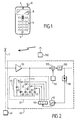
- FIG. 1 there is shown an electronic device according to the invention.
- a wireless telephone device of the CT0 type or others is composed of a microphone 5, an earphone 6, a screen 8, a keyboard 9 and an antenna 11.
- This device is connected to its base, not shown in the figure, using a frequency channel. It should be noted that the invention can also be applied to the base itself.
- FIG. 2 shows on one side the transmission part 40, which is not detailed because it is not part of the invention and the reception part 45. It is in this reception part that the selective amplifier is located which is the high frequency preamplifier .
- This amplifier is shown schematically in this figure by an amplifier 50, proper, at the output of which a selective circuit 51 of the plug circuit type is provided.
- This plug circuit is formed by a self-induction coil 55 at the ends of which is connected a main capacitor 65 which fixes as a first approximation the tuning frequency of this plug circuit.
- This capacitor can also be a diode with variable capacity.
- capacitors 68, 69, 70 and 71 are provided.
- they can be paralleled on the main capacitor 65 by a connection circuit constituted by switch circuits 78, 79, 80 and 81 respectively.
- the open or closed position of these switch circuits is determined by the contents of a counter 90.
- the content of this counter 90 is incremented under the control of a microprocessor 92, as well as its zeroing.
- This microprocessor also receives a signal from a level detector 98.
- This level detector is connected to the output of a medium frequency filter 100.
- This filter shows a medium frequency signal obtained by a mixer 105 which performs mixing the signals supplied by the selective amplifier 50 provided with the cap circuit 51 and a local oscillator 110.
- a reference transmitter 150 is used to adjust the capacity to be connected to the main capacitor 65. Capacitors are connected in parallel in parallel to the plug circuit. The combination applied on this plug circuit which gives the best received level is stored, for example, by freezing the contents of the counter 90.
- contents of the counter 90 are stored for different frequencies developed by the reference oscillator 150 so that the different carriers that the apparatus can receive can be adjusted.
- capacitors have been cited for adjusting the oscillating circuit, it is also possible to use reactive elements produced by inductance inductors without departing from the scope of the invention.
Description
La présente invention concerne un appareil radioélectrique comportant une partie réception formée par au moins :
- un étage amplificateur sélectif haute fréquence muni d'un circuit sélectif accordable sur une certaine bande de fréquence.
- a high frequency selective amplifier stage provided with a selective circuit tunable over a certain frequency band.
L'invention concerne aussi un procédé pour régler un des étages amplificateurs haute fréquence contenu dans un tel appareil.The invention also relates to a method for adjusting one of the high frequency amplifier stages contained in such an apparatus.
De tels appareils sont bien connus et trouvent de nombreuses applications, notamment dans le domaine des appareils de téléphonie portable. Il est nécessaire pour ce genre d'appareil d'avoir un récepteur sensible ce qui augmente sa portée. L'utilisation d'amplificateur sélectif améliore la sensibilité.Such devices are well known and find many applications, especially in the field of portable telephony devices. It is necessary for this kind of device to have a sensitive receiver which increases its range. The use of selective amplifier enhances sensitivity.
Un problème qui se pose avec de tels appareils, est l'accord de cet amplificateur sélectif. En cours de fabrication, on utilise des composants dont les valeurs présentent une certaine dispersion. On se trouve alors confronté au fait que la fréquence d'accord des amplificateurs sélectifs varie d'un exemplaire à l'autre en fin de fabrication et varie aussi en fonction de la température. Pour compenser cela, il est d'usage de prévoir un condensateur de réglage et d'agir sur sa valeur afin que le circuit sélectif soit bien accordé sur la bande de fréquences dans laquelle il doit travailler. Une compensation en température est décrite dans le document de brevet japonais publié le 24.01.1995 sous le numéro 07022974. Cette compensation agit sur une diode à capacité variable qui accorde aussi le circuit oscillant de sorte que la variation totale que l'on peut appliquer à cette diode est obérée de cette compensation.A problem that arises with such devices is the tuning of this selective amplifier. In the course of manufacture, components whose values have a certain dispersion are used. We are then faced with the fact that the tuning frequency of the selective amplifiers varies from one copy to another at the end of manufacture and also varies according to the temperature. To compensate for this, it is customary to provide a tuning capacitor and act on its value so that the selective circuit is tuned to the frequency band in which it must work. Temperature compensation is described in Japanese Patent Publication No. 07022974 published on 24.01.1995. This compensation acts on a variable capacitance diode which also provides the oscillating circuit so that the total variation that can be applied to this diode is obedient to this compensation.
Le document EP-A 0 546 723 décrit aussi un circuit sélectif accordable par une grandeur de commande. Le réglage de ce circuit est effectué pendant le fonctionnement de l'appareil auquel il est rattaché. On n'est pas confronté au problème de réglage des appareils en fin de fabrication.EP-
La présente invention propose un appareil du genre mentionné dans le préambule dans lequel on a prévu des moyens pour faciliter l'accord de l'étage sélectif sans utiliser de mesureur de température notamment et des moyens pour maintenir la dynamique de la tension applicable à la tension d'accord si le circuit sélectif exige une certaine dynamique dans l'accord de son circuit sélectif.The present invention provides an apparatus of the type mentioned in the preamble in which there are provided means for facilitating the tuning of the selective stage without using a particular temperature meter and means for maintaining the dynamic voltage applicable to the voltage agree if the selective circuit requires some dynamics in the tuning of its selective circuit.
Pour cela, un tel appareil est remarquable en ce qu'il est prévu :
- un mesureur de niveau reçu pour mesurer le niveau reçu des signaux émis par un oscillateur de référence placé à l'extérieur dudit appareil et mis en oeuvre en fin de fabrication dudit appareil,
- un organe de variation pour faire varier ladite bande de fréquence en fonction d'une grandeur de commande, organe comprenant une pluralité d'éléments réactifs et un réseau de connexion pour brancher sur le circuit sélectif accordable au moins un élément réactif dudit ensemble en fonction de ladite grandeur de commande
- un organe de mise en mémoire de la grandeur de commande qui donne le meilleur niveau obtenu par le mesureur de niveau, grandeur de commande utilisée durant le fonctionnement normal dudit appareil.
- a received level meter for measuring the received level of the signals emitted by a reference oscillator placed outside said apparatus and implemented at the end of manufacture of said apparatus,
- a variation member for varying said frequency band as a function of a control quantity, which member comprises a plurality of reactive elements and a connection network for connecting to the tunable selective circuit at least one reactive element of said set as a function of said control quantity
- a controller for storing the control quantity which gives the best level obtained by the level meter, control variable used during the normal operation of said apparatus.
Une des idées de l'invention est d'insérer dans le circuit sélectif un ou plusieurs éléments réactifs qui permettent de centrer ce circuit sélectif sur la plage de fréquence sur laquelle l'appareil est censé fonctionner.One of the ideas of the invention is to insert in the selective circuit one or more reactive elements that allow to center this selective circuit on the frequency range on which the device is supposed to operate.
La description suivante, faite en regard des dessins ci-annexés, le tout donné à titre d'exemple non limitatif, fera bien comprendre comment l'invention peut être réalisée.
- La figure 1 montre un appareil conforme à l'invention.
- La figure 2 montre le détail de réalisation de l'invention.
- La figure 3 est un organigramme destiné à expliciter le fonctionnement de l'invention.
- Figure 1 shows an apparatus according to the invention.
- Figure 2 shows the detail of the invention.
- Figure 3 is a flowchart for explaining the operation of the invention.
A la figure 1, on a représenté un appareil électronique conforme à l'invention. Dans le cadre de l'exemple décrit c'est un appareil téléphonique sans fil du genre CT0 ou autres. Il est composé d'un microphone 5, d'un écouteur 6, d'un écran 8, d'un clavier 9 et d'une antenne 11. Cet appareil se raccorde à sa base, non représentée sur la figure, en utilisant un canal de fréquence. Il est à noter que l'invention peut aussi s'appliquer à la base elle-même.In Figure 1, there is shown an electronic device according to the invention. In the context of the example described is a wireless telephone device of the CT0 type or others. It is composed of a
La figure 2 montre d'un côté la partie émission 40, non détaillée car ne faisant pas partie de l'invention et la partie réception 45. C'est dans cette partie réception que se trouve l'amplificateur sélectif qui est le préamplificateur haute fréquence. Cet amplificateur est représenté schématiquement sur cette figure par un amplificateur 50, proprement dit, à la sortie duquel un circuit sélectif 51 du genre circuit bouchon est prévu. Ce circuit bouchon est formé par une bobine de self induction 55 aux extrémités de laquelle est branché un condensateur principal 65 qui fixe en première approximation la fréquence d'accord de ce circuit bouchon. Ce condensateur peut être aussi une diode à capacité variable.FIG. 2 shows on one side the transmission part 40, which is not detailed because it is not part of the invention and the
Selon l'invention, pour faire varier la fréquence d'accord de ce circuit sélectif, d'autres condensateurs 68, 69, 70 et 71 sont prévus. Pour cela, ils peuvent être mis en parallèle sur le condensateur principal 65 par un circuit de connexion constitué par des circuits interrupteurs 78, 79, 80 et 81 respectivement. La position ouverte ou fermée de ces circuits interrupteurs est déterminée par le contenu d'un compteur 90. Le contenu de ce compteur 90 s'incrémente sous la commande d'un microprocesseur 92, ainsi que sa mise à zéro. Ainsi, l'ensemble formé par les condensateurs 68, 69, 70 et 71, les circuits interrupteurs 78, 79, 80 et 81 constitue un organe de variation de la fréquence d'accord commandé par le contenu du compteur 90. Ce microprocesseur reçoit aussi un signal en provenance d'un détecteur de niveau 98. Ce détecteur de niveau est branché à la sortie d'un filtre de moyenne fréquence 100. Ce filtre met en évidence un signal de moyenne fréquence obtenu par un mélangeur 105 qui effectue le mélange des signaux fournis par l'amplificateur sélectif 50 muni du circuit bouchon 51 et d'un oscillateur local 110. Pour effectuer le réglage de la capacité à mettre en parallèle au condensateur principal 65, on utilise un émetteur de référence 150. Les différents condensateurs sont branchés tour à tour en parallèle sur le circuit bouchon. La combinaison appliquée sur ce circuit bouchon qui donne le meilleur niveau reçu est emmagasinée, par exemple, en figeant le contenu du compteur 90.According to the invention, to vary the tuning frequency of this selective circuit, other capacitors 68, 69, 70 and 71 are provided. For this, they can be paralleled on the
La figure 3 est un organigramme qui explicite le fonctionnement de l'invention. La case K0 indique l'entrée du processus de réglage de la valeur des capacités à insérer dans le circuit oscillant 51. Ce processus est mis en oeuvre principalement par le microprocesseur 92. La case K1 indique l'initialisation de deux variables : tout d'abord la variable C qui est le contenu du compteur 90, c'est-à-dire que le contenu de ce compteur 90 est mis à zéro, et une variable N destinée à contenir la valeur du niveau mesuré par le détecteur 98. A la case K3, on recueille la valeur du niveau détecté. Ce niveau est dû à l'émission de l'émetteur de référence 105 mis en route au préalable. Ce niveau est ensuite comparé comme indiqué à la case K5 avec le niveau enregistré dans la variable N. Si le niveau Nc qui vient d'être fourni est supérieur à la valeur déjà enregistrée, alors cette dernière valeur de Nc est emmagasinée dans la variable N. En outre la valeur du contenu du compteur 90 est stockée dans une variable CM (case K8). Après l'opération effectuée dans la case K8 et si le test indiqué à la case K5 est négatif, alors on effectue un test sur le contenu C du compteur 90. On teste donc si ce contenu est égal à 15, case K10, ce qui correspond à un compteur à 4 positions qui compte, en binaire, de 0000 à 1111. Si le contenu de 15 n'est pas obtenu, alors on incrémente ce compteur d'une unité, case K12. Si ce contenu est égal à 15, alors on charge la valeur CM qui est associée donc au plus haut niveau détecté, case K14. La case K15 marque la fin de l'exécution du programme après l'opération de la case K14. Les valeurs C68, C69, C70 et C71 des condensateurs 68, 69, 70 et 71 respectivement sont doubles l'une de l'autre telles que :
- C68 = 1.CO
- C69 = 2.CO
- C70 = 4.CO
- C71 = 8.CO
- C68 = 1.CO
- C69 = 2.CO
- C70 = 4.CO
- C71 = 8.CO
En variante, il est possible que des contenus du compteur 90 soient mémorisés pour différentes fréquences élaborées par l'oscillateur de référence 150 de sorte que l'on puisse s'ajuster sur les différentes porteuses que l'appareil peut recevoir.Alternatively, it is possible that contents of the
Bien que l'on ait cité des condensateurs pour régler le circuit oscillant, on peut aussi utiliser des éléments réactifs réalisés par des self inductances sans pour cela sortir du cadre de l'invention.Although capacitors have been cited for adjusting the oscillating circuit, it is also possible to use reactive elements produced by inductance inductors without departing from the scope of the invention.
Claims (4)
- A radio device comprising a receiving part formed by at least:- a selective high-frequency amplifier stage including a selective circuit that can be tuned to a certain frequency band,characterized in that there is provided:- a received level meter for measuring the received level of the signals transmitted by a reference oscillator placed on the outside of said device and used at the end of the manufacture of said device,- a variation element for causing said frequency band to vary as a function of a control magnitude, the element comprising a plurality of reactive elements and a connecting network to connect to the selective tuning circuit at least one reactive element of said set as a function of said control magnitude,- a storage element for storing the control magnitude that gives the best level obtained by the level meter, which control magnitude is used during the normal operation of said device.
- A device as claimed in claim 1, characterized in that the variation element is further formed by a counter for alternately connecting each and every combination of groups of reactive elements.
- A device as claimed in claim 1 or 2, characterized in that the reactive elements are capacitors.
- A method of adjusting at least one of the high-frequency amplifier stages of a receiver, including a selective circuit, the method being implemented in a device as claimed in one of the claims 1 to 3, characterized in that for determining the connection of reactive correction elements for the selective circuit, it comprises the following steps:- application of a signal of a reference oscillator,- alternate connection of each reactive element and/or each and every combination of groups of reactive elements,- measurement of the level received on the output of the amplifier circuit,- storage of the element or of the group giving the best level.
Applications Claiming Priority (2)
| Application Number | Priority Date | Filing Date | Title |
|---|---|---|---|
| FR9804730 | 1998-04-16 | ||
| FR9804730 | 1998-04-16 |
Publications (2)
| Publication Number | Publication Date |
|---|---|
| EP0951147A1 EP0951147A1 (en) | 1999-10-20 |
| EP0951147B1 true EP0951147B1 (en) | 2007-03-28 |
Family
ID=9525294
Family Applications (1)
| Application Number | Title | Priority Date | Filing Date |
|---|---|---|---|
| EP99201099A Expired - Lifetime EP0951147B1 (en) | 1998-04-16 | 1999-04-07 | Receiver and a method for tuning one of the radio frequency stages in a receiver |
Country Status (6)
| Country | Link |
|---|---|
| US (1) | US6408167B1 (en) |
| EP (1) | EP0951147B1 (en) |
| JP (1) | JP2000004180A (en) |
| KR (1) | KR100640669B1 (en) |
| CN (1) | CN1132310C (en) |
| DE (1) | DE69935632T2 (en) |
Families Citing this family (8)
| Publication number | Priority date | Publication date | Assignee | Title |
|---|---|---|---|---|
| GB9916901D0 (en) | 1999-07-19 | 1999-09-22 | Cambridge Silicon Radio Ltd | Adjustable filter |
| AU2000266379A1 (en) * | 1999-08-10 | 2004-01-06 | Qualcomm Incorporated | Band switchable intermediate frequency band pass filter |
| FR2811189B1 (en) * | 2000-06-29 | 2002-09-06 | Sagem | DEVICE FOR RECEIVING A RADIO FREQUENCY SIGNAL IN A MOBILE TELEPHONE |
| US6985702B2 (en) * | 2001-02-23 | 2006-01-10 | Koninklijke Philips Electronics N.V. | Transceiver with frequency multiplier tracked to frequency generator |
| US6915114B2 (en) * | 2002-05-07 | 2005-07-05 | Broadcom, Corp. | Direct tuning of embedded integrated circuit components |
| US20050040909A1 (en) * | 2003-08-20 | 2005-02-24 | Waight Matthew Glenn | Broadband integrated digitally tunable filters |
| JP4805317B2 (en) * | 2008-02-20 | 2011-11-02 | 旭化成エレクトロニクス株式会社 | Communications system |
| JP4751427B2 (en) * | 2008-08-08 | 2011-08-17 | 旭化成エレクトロニクス株式会社 | Communications system |
Family Cites Families (11)
| Publication number | Priority date | Publication date | Assignee | Title |
|---|---|---|---|---|
| US4186360A (en) * | 1977-02-18 | 1980-01-29 | Sanyo Electric Co., Ltd. | Digital channel selecting apparatus |
| JPH0448827A (en) * | 1990-06-16 | 1992-02-18 | Nec Corp | Radio selective calling receiver |
| JP2758712B2 (en) * | 1990-10-12 | 1998-05-28 | 日本電気株式会社 | Radio selective call receiver |
| JP2852132B2 (en) * | 1991-01-17 | 1999-01-27 | 日本電気株式会社 | Radio selective call receiver |
| US5369793A (en) * | 1991-12-12 | 1994-11-29 | Raytheon Company | RF receiver adapted to process received RF pulses and reject RF continuous wave signals |
| US5548821A (en) * | 1992-06-09 | 1996-08-20 | Coveley; Michael | Adaptive system for self-tuning and selecting a carrier frequency in a radio frequency communication system |
| FI94689C (en) * | 1992-12-10 | 1995-10-10 | Nokia Mobile Phones Ltd | Reconciliation of tuning circuits in a radio receiver |
| JP2951156B2 (en) | 1993-06-29 | 1999-09-20 | 三洋電機株式会社 | Temperature compensated radio receiver |
| FR2722339B1 (en) * | 1994-07-06 | 1996-10-04 | Tech D Applic & De Rech Electr | FAST AUTOMATIC HALF-LOOP ANTENNA |
| US6081700A (en) * | 1996-12-17 | 2000-06-27 | Motorola, Inc. | Radio having a self-tuning antenna and method thereof |
| US6058294A (en) * | 1998-03-24 | 2000-05-02 | Microchip Technology Incorporated | Adjustable frequency stabilizing internal chip capacitor system |
-
1999
- 1999-04-07 DE DE69935632T patent/DE69935632T2/en not_active Expired - Lifetime
- 1999-04-07 EP EP99201099A patent/EP0951147B1/en not_active Expired - Lifetime
- 1999-04-12 US US09/289,846 patent/US6408167B1/en not_active Expired - Lifetime
- 1999-04-13 JP JP11104683A patent/JP2000004180A/en active Pending
- 1999-04-13 CN CN99105086A patent/CN1132310C/en not_active Expired - Fee Related
- 1999-04-16 KR KR1019990013468A patent/KR100640669B1/en not_active IP Right Cessation
Also Published As
| Publication number | Publication date |
|---|---|
| JP2000004180A (en) | 2000-01-07 |
| EP0951147A1 (en) | 1999-10-20 |
| KR100640669B1 (en) | 2006-11-02 |
| CN1132310C (en) | 2003-12-24 |
| US6408167B1 (en) | 2002-06-18 |
| DE69935632T2 (en) | 2007-10-04 |
| DE69935632D1 (en) | 2007-05-10 |
| KR19990083240A (en) | 1999-11-25 |
| CN1235416A (en) | 1999-11-17 |
Similar Documents
| Publication | Publication Date | Title |
|---|---|---|
| EP2469783B1 (en) | FSK radio signal receiver with high-sensitivity demodulator and method for operating said receiver | |
| EP2509222B1 (en) | Channel for radio-frequency transmission or reception, with automatic impedance matching and corresponding method | |
| EP0951147B1 (en) | Receiver and a method for tuning one of the radio frequency stages in a receiver | |
| FR2473818A1 (en) | DOUBLE SUPERHETERODYNE RECEIVER | |
| FR2949922A1 (en) | MULTIBAND ANTENNA IMPEDANCE ADAPTATION METHOD AND AUTOMATICALLY ADAPTABLE TRANSMISSION OR RECEPTION CHAIN. | |
| EP0792027B1 (en) | Multi-band radio-telephone apparatus | |
| BE1012885A3 (en) | With channel selection power function preset auto. | |
| EP0944171A1 (en) | Electronic apparatus comprising a frequency synthesizer and process for adjusting a frequency synthesizer | |
| EP0034064B1 (en) | Adjustable and selective electrical filters and methods of tuning them | |
| EP1608073B1 (en) | Voltage controlled oscillator | |
| FR2786342A1 (en) | Frequency doubling method for frequency synthesizer, involves decreasing local intermediate frequency in units of 50 kHz and increasing local radio frequency in units of 25 kHz. | |
| EP1295391A1 (en) | Self-adaptive frequency band-pass filtering device in microwave signal transceiver | |
| FR2666709A1 (en) | GAIN ADJUSTMENT ASSEMBLY FOR RADIOTELEPHONE. | |
| FR2791840A1 (en) | FSK radio transceiver with common PLL circuit on transmit and receive, supplies quadrature outputs from VCO to receiver mixers feeding lowpass filters and amplifiers | |
| EP0143041A2 (en) | Device for the compensation of the acceleration sensitivity of an oscillator | |
| EP2009790B1 (en) | Method for tuning the resonant frequency of an antenna | |
| FR2906630A1 (en) | DEVICE FOR INTERROGATION OF A PASSIVE SENSOR OF ACOUSTIC SURFACE WAVE TYPE. | |
| EP3163758B1 (en) | Radio frequency signal receiver device, control method for such a device and corresponding computer program | |
| EP1052772B1 (en) | Circuit and method for producing a filtered signal | |
| EP0954097A1 (en) | Adjustable bandpass filter | |
| FR2867926A1 (en) | SATELLITE RECEPTION METHOD AND SYSTEM | |
| FR2893802A1 (en) | Frequency shift keying frequency modulated radiofrequency signal demodulation device for radio receiver, has mixer to convert signal`s radiofrequency into intermediate frequency and with output followed by filtering and amplifier circuits | |
| EP0989682A1 (en) | Mobile telephone transceiver | |
| FR2488078A1 (en) | Servo-controlled RF band pass filter - has voltage tuned inductors switched to resonant oscillator mode and tracked to reference oscillator to determine control voltage | |
| FR2670063A1 (en) | Analog frequency/phase detector and its use in a phase-locked loop |
Legal Events
| Date | Code | Title | Description |
|---|---|---|---|
| PUAI | Public reference made under article 153(3) epc to a published international application that has entered the european phase |
Free format text: ORIGINAL CODE: 0009012 |
|
| AK | Designated contracting states |
Kind code of ref document: A1 Designated state(s): DE ES FR GB IT |
|
| AX | Request for extension of the european patent |
Free format text: AL;LT;LV;MK;RO;SI |
|
| RTI1 | Title (correction) |
Free format text: RECEIVER AND A METHOD FOR TUNING ONE OF THE RADIO FREQUENCY STAGES IN A RECEIVER |
|
| 17P | Request for examination filed |
Effective date: 20000420 |
|
| AKX | Designation fees paid |
Free format text: DE ES FR GB IT |
|
| GRAP | Despatch of communication of intention to grant a patent |
Free format text: ORIGINAL CODE: EPIDOSNIGR1 |
|
| GRAS | Grant fee paid |
Free format text: ORIGINAL CODE: EPIDOSNIGR3 |
|
| GRAA | (expected) grant |
Free format text: ORIGINAL CODE: 0009210 |
|
| AK | Designated contracting states |
Kind code of ref document: B1 Designated state(s): DE ES FR GB IT |
|
| REG | Reference to a national code |
Ref country code: GB Ref legal event code: FG4D Free format text: NOT ENGLISH |
|
| REF | Corresponds to: |
Ref document number: 69935632 Country of ref document: DE Date of ref document: 20070510 Kind code of ref document: P |
|
| PG25 | Lapsed in a contracting state [announced via postgrant information from national office to epo] |
Ref country code: ES Free format text: LAPSE BECAUSE OF FAILURE TO SUBMIT A TRANSLATION OF THE DESCRIPTION OR TO PAY THE FEE WITHIN THE PRESCRIBED TIME-LIMIT Effective date: 20070709 |
|
| GBT | Gb: translation of ep patent filed (gb section 77(6)(a)/1977) |
Effective date: 20070620 |
|
| RAP2 | Party data changed (patent owner data changed or rights of a patent transferred) |
Owner name: NXP B.V. |
|
| PLBE | No opposition filed within time limit |
Free format text: ORIGINAL CODE: 0009261 |
|
| STAA | Information on the status of an ep patent application or granted ep patent |
Free format text: STATUS: NO OPPOSITION FILED WITHIN TIME LIMIT |
|
| 26N | No opposition filed |
Effective date: 20080102 |
|
| PG25 | Lapsed in a contracting state [announced via postgrant information from national office to epo] |
Ref country code: IT Free format text: LAPSE BECAUSE OF FAILURE TO SUBMIT A TRANSLATION OF THE DESCRIPTION OR TO PAY THE FEE WITHIN THE PRESCRIBED TIME-LIMIT Effective date: 20070328 |
|
| REG | Reference to a national code |
Ref country code: GB Ref legal event code: 732E |
|
| REG | Reference to a national code |
Ref country code: FR Ref legal event code: TP |
|
| PGFP | Annual fee paid to national office [announced via postgrant information from national office to epo] |
Ref country code: GB Payment date: 20100325 Year of fee payment: 12 |
|
| PGFP | Annual fee paid to national office [announced via postgrant information from national office to epo] |
Ref country code: FR Payment date: 20100521 Year of fee payment: 12 |
|
| PGFP | Annual fee paid to national office [announced via postgrant information from national office to epo] |
Ref country code: DE Payment date: 20100430 Year of fee payment: 12 |
|
| REG | Reference to a national code |
Ref country code: DE Ref legal event code: R119 Ref document number: 69935632 Country of ref document: DE |
|
| REG | Reference to a national code |
Ref country code: DE Ref legal event code: R119 Ref document number: 69935632 Country of ref document: DE |
|
| GBPC | Gb: european patent ceased through non-payment of renewal fee |
Effective date: 20110407 |
|
| REG | Reference to a national code |
Ref country code: FR Ref legal event code: ST Effective date: 20111230 |
|
| PG25 | Lapsed in a contracting state [announced via postgrant information from national office to epo] |
Ref country code: FR Free format text: LAPSE BECAUSE OF NON-PAYMENT OF DUE FEES Effective date: 20110502 |
|
| PG25 | Lapsed in a contracting state [announced via postgrant information from national office to epo] |
Ref country code: GB Free format text: LAPSE BECAUSE OF NON-PAYMENT OF DUE FEES Effective date: 20110407 |
|
| PG25 | Lapsed in a contracting state [announced via postgrant information from national office to epo] |
Ref country code: DE Free format text: LAPSE BECAUSE OF NON-PAYMENT OF DUE FEES Effective date: 20111031 |