EP2009790B1 - Method for tuning the resonant frequency of an antenna - Google Patents
Method for tuning the resonant frequency of an antenna Download PDFInfo
- Publication number
- EP2009790B1 EP2009790B1 EP08158734A EP08158734A EP2009790B1 EP 2009790 B1 EP2009790 B1 EP 2009790B1 EP 08158734 A EP08158734 A EP 08158734A EP 08158734 A EP08158734 A EP 08158734A EP 2009790 B1 EP2009790 B1 EP 2009790B1
- Authority
- EP
- European Patent Office
- Prior art keywords
- signal
- transmission
- phase shift
- resonant circuit
- frequency
- Prior art date
- Legal status (The legal status is an assumption and is not a legal conclusion. Google has not performed a legal analysis and makes no representation as to the accuracy of the status listed.)
- Active
Links
- 238000000034 method Methods 0.000 title claims description 12
- 230000005540 biological transmission Effects 0.000 claims description 132
- 230000010363 phase shift Effects 0.000 claims description 75
- 238000005259 measurement Methods 0.000 claims description 64
- 239000003990 capacitor Substances 0.000 claims description 24
- 238000001514 detection method Methods 0.000 claims description 21
- 230000001939 inductive effect Effects 0.000 claims description 12
- 238000004804 winding Methods 0.000 claims description 6
- 238000001914 filtration Methods 0.000 claims description 5
- 230000003044 adaptive effect Effects 0.000 claims description 3
- 238000012886 linear function Methods 0.000 claims description 2
- 230000010287 polarization Effects 0.000 claims 1
- 235000021183 entrée Nutrition 0.000 description 8
- 230000006870 function Effects 0.000 description 8
- 238000010586 diagram Methods 0.000 description 6
- 230000004044 response Effects 0.000 description 4
- 238000005516 engineering process Methods 0.000 description 3
- 238000004891 communication Methods 0.000 description 2
- 230000014509 gene expression Effects 0.000 description 2
- 238000002347 injection Methods 0.000 description 2
- 239000007924 injection Substances 0.000 description 2
- 230000004048 modification Effects 0.000 description 2
- 238000012986 modification Methods 0.000 description 2
- 101100536354 Drosophila melanogaster tant gene Proteins 0.000 description 1
- 230000004888 barrier function Effects 0.000 description 1
- 230000008859 change Effects 0.000 description 1
- 238000011161 development Methods 0.000 description 1
- 238000006073 displacement reaction Methods 0.000 description 1
- 239000003607 modifier Substances 0.000 description 1
- 230000000737 periodic effect Effects 0.000 description 1
- 230000009131 signaling function Effects 0.000 description 1
- 238000001228 spectrum Methods 0.000 description 1
- 230000007480 spreading Effects 0.000 description 1
- 230000001360 synchronised effect Effects 0.000 description 1
- 230000002277 temperature effect Effects 0.000 description 1
- 238000012546 transfer Methods 0.000 description 1
Images


Classifications
-
- H—ELECTRICITY
- H03—ELECTRONIC CIRCUITRY
- H03J—TUNING RESONANT CIRCUITS; SELECTING RESONANT CIRCUITS
- H03J3/00—Continuous tuning
- H03J3/02—Details
- H03J3/06—Arrangements for obtaining constant bandwidth or gain throughout tuning range or ranges
- H03J3/08—Arrangements for obtaining constant bandwidth or gain throughout tuning range or ranges by varying a second parameter simultaneously with the tuning, e.g. coupling bandpass filter
-
- H—ELECTRICITY
- H03—ELECTRONIC CIRCUITRY
- H03J—TUNING RESONANT CIRCUITS; SELECTING RESONANT CIRCUITS
- H03J2200/00—Indexing scheme relating to tuning resonant circuits and selecting resonant circuits
- H03J2200/10—Tuning of a resonator by means of digitally controlled capacitor bank
-
- H—ELECTRICITY
- H04—ELECTRIC COMMUNICATION TECHNIQUE
- H04B—TRANSMISSION
- H04B5/00—Near-field transmission systems, e.g. inductive or capacitive transmission systems
- H04B5/20—Near-field transmission systems, e.g. inductive or capacitive transmission systems characterised by the transmission technique; characterised by the transmission medium
- H04B5/24—Inductive coupling
-
- H—ELECTRICITY
- H04—ELECTRIC COMMUNICATION TECHNIQUE
- H04B—TRANSMISSION
- H04B5/00—Near-field transmission systems, e.g. inductive or capacitive transmission systems
- H04B5/40—Near-field transmission systems, e.g. inductive or capacitive transmission systems characterised by components specially adapted for near-field transmission
- H04B5/45—Transponders
Definitions
- the present invention relates to a transmission / reception device of a near-field transmission system, said transmission / reception device comprising a transmission / reception unit connected to a resonant circuit comprising at least one inductive element serving as a antenna to said transmitting / receiving device for transmitting a modulated signal delivered by said transmitting / receiving unit or for receiving transmission signals.
- the present invention relates to a method for tuning the resonant frequency of a resonant circuit comprising at least one inductive element serving as antenna of a transmission / reception device of a near-field transmission system on the frequency transmission / reception of said transmitting / receiving device.
- NFC Near Field Communication
- the mobile device is then called “tag” while the terminal is generally called “receiver”.
- the tag transmits to the latter identification information that can then be used to open a barrier, to authorize a particular operation, etc.
- the mobile device can be a dedicated device or, as it exists today, a specially equipped mobile phone.
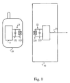
- a mobile device 10 which may for example be a mobile telephone, and, on the other hand, an access terminal 20.
- the mobile device 10 is equipped with a transmitting / receiving unit 11 which is connected to a resonant circuit 12, consisting of an inductor 121 and a capacitor 122.
- the access terminal 20 is equipped with a transmission / reception unit 21 which is connected to a circuit resonant 22 itself consisting of an inductor 221 and a capacitor 222.
- the transmitting / receiving unit 21 of the access terminal 20 is connected by a link 23 to an information center (no represent).
- the resonant circuit 12 or 22 of the one of these devices which operates as a transmitter radiates in the near field a magnetic field which is received by the other resonant circuit 22. (respectively 12).
- the transmission / reception units 11 and 21 comprise modulation / demodulation circuits (not shown) so that information in the form of modulated signals can be exchanged between the mobile device 10 and the access terminal 20 and vice versa.
- each of the resonant circuits 12 and 22 is constituted, as can be seen in FIG. Fig. 1 , by an inductance 121, 221 and a capacitor 122, 222 whose values are such that they form between them a resonant circuit at the transmission frequency of these modulated signals.
- Such a resonant circuit is characterized at a frequency given by its quality factor, generally denoted Q, which has, as a function of frequency, a bell-shaped curve with a maximum value obtained for the resonance frequency of the resonant circuit.
- Q quality factor
- the greater the distance between the mobile device 10 and the access terminal 20 below which the transmission is provided is important, the higher the quality factor of each resonant circuit. To do this, we therefore seeks to be at a transmission frequency as close as possible to the resonant frequency of each resonant circuit.
- Such a resonant circuit is disclosed by the European patent EP 0 663 724 .
- Each resonant circuit can be disturbed and its agreement be modified, with a correlative decrease in its quality factor, by the presence of objects in the vicinity, such as metallic objects which significantly modify the value of the inductance of the circuit, but also by temperature effects.
- the object of the present invention is to propose a method for solving the problems mentioned above and thus to provide such a device at least one of the resonant circuits is provided with adaptive tuning means so as to always work at a value as close as possible to its maximum quality factor.
- the present invention also relates to a transmitting / receiving device of a near-field transmission system.
- Said transmission / reception device is of the type which comprises a transmission / reception unit connected to a resonant circuit comprising at least one inductive element serving as an antenna for said transmitting / receiving device for transmitting a modulated signal delivered by said transmitting / receiving unit or for receiving transmission signals.
- said transmitting / receiving device further comprises a phase shift measuring unit provided for, on the one hand, measuring the phase shift experienced by said resonant circuit, the modulated signal delivered by said unit transmission / reception or the signal generated in said inductive element on receiving transmission signals and, on the other hand, outputting a control signal to means included in said resonant circuit for modifying its resonant frequency, said signal of control tending to cancel said phase shift.
- a phase shift measuring unit provided for, on the one hand, measuring the phase shift experienced by said resonant circuit, the modulated signal delivered by said unit transmission / reception or the signal generated in said inductive element on receiving transmission signals and, on the other hand, outputting a control signal to means included in said resonant circuit for modifying its resonant frequency, said signal of control tending to cancel said phase shift.
- said modulator consists of a multiplier receiving on its inputs the signals generated by said first and second generators, a filter whose input is connected to the output of said multiplier, said filter being arranged to filter one of the sidebands of the output signal of said multiplier and to pass the other sideband, the measurement signal being the output signal of said filter.
- said modulator consists of a first and a second multiplier and a first and a second phase shifter of ⁇ / 2, said first multiplier receiving, on an input, the generated signal by said first generator and, on the other input, the signal generated by said second generator after phase shift in said second phase-shifter and said second multiplier receiving, on an input, the signal generated by said second generator and, on the other input, the signal generated by said first generator after phase shift in said first phase-shifter, the output of each multiplier being connected to the input of an adder or difference-producing unit whose output delivers said measurement signal.
- said detection unit in a first embodiment, it consists of a multiplier receiving on its inputs the measurement signal after passing through said resonant circuit and the signal generated by said second generator and a filter whose The input is connected to the output of said multiplier, said filter being provided for filtering one of the sidebands of the output signal of said multiplier and for passing the other sideband.
- said detection unit in a second embodiment, it consists of a first and a second multiplier and a first and a second phase shifter of ⁇ / 2, said first multiplier receiving, on an input, the measurement signal after passing through said resonant circuit and, on the other input, the signal generated by said second generator after phase shift in said second phase-shifter and said second multiplier receiving, on an input, the signal generated by said second generator and, on the other input, the signal measured after passing through said resonant circuit after phase shift in said first phase-shifter, the output of each multiplier being connected to the input of an adder or a unit making the difference.
- said phase-shifting unit comprises a servo unit which receives on its input the phase-shift signal and which delivers a bias signal of said control means.
- said resonant circuit whose amplitude is such that said measured phase shift is zero.
- said resonant circuit comprises an inductance coupled in parallel with a capacitance, said inductor serving as an antenna for said transmitting / receiving device.
- said resonant circuit comprises a transformer with symmetrical windings, said windings being coupled in parallel to these capacitors of the same value, said transformer serving as an antenna to said transmitting / receiving device.
- At least one capacitor of said resonant circuit is a variable capacity per control.
- Said capacitance then consists of several capacitors which can, switchably by means of switching elements, be connected in parallel with at least one other.
- each switching element is driven by one of the output bits of an analog-digital converter receiving the phase shift signal delivered by said phase shift measuring unit.
- said first generator is a sinusoidal signal generator.
- said second generator is a sinusoidal signal generator.
- said second generator is a pseudo-random sequence generator, for example, which uses to transmit said sequences a primitive generator polynomial modulo 2.
- the present invention is based on the phase characteristics exhibited by an RLC resonant circuit such as that shown in FIG. Fig. 2a in which a resistor R is connected, by a terminal, to the source Ve and, by the other terminal, to the common point between an inductance L and a capacitance C, which are themselves connected in parallel with each other and at the terminals of which is taken the output voltage Vs.
- the amplitude maximum is reached for a frequency f 0 , called the resonance frequency.
- the resonance factor is denoted by Q and represents the ratio of the output and input amplitudes of the resonant circuit.
- the curve of the Fig. 2c which shows the phase response of the resonant circuit RLC as a function of the frequency, at the resonance frequency f 0 , the phase shift introduced by the RLC circuit is zero.
- the principle of the present invention is based on this finding.
- the invention proposes to make a measurement of the phase shift introduced by this resonant circuit on said transmission signals and to modify the resonant frequency of said resonant circuit so that this phase shift is zero.
- a transmitting / receiving device of a transmission system according to the present invention as illustrated in FIG. Fig. 4 comprises a transmission / reception unit 31 connected to a resonant circuit 32 which consists of a resistor 323 connected in series with an inductor 321 forming an antenna for the transmission system and a capacitor 322 in parallel with the inductor 321.
- common terminals Bc of the inductor 321 and the capacitor 322 are connected via the resistor 323 to the terminal Su of the transmitting / receiving unit 31 while the other common terminal is connected to ground to which is also connected the transmitting / receiving unit 31 by its ground terminal SM.
- the resistor 323, the inductor 321 and the capacitor 322 respectively have such values that the resonant circuit 32 can resonate at the nominal frequency of the transmission system or at a frequency close to said nominal frequency.
- the inductance 321 and the capacitance 322 are, one and / or the other, variable by application of a command from a phase-shifter measuring unit 33 so that the resonance frequency of said resonant circuit 32 may vary. In this case, only the capacity 322 is variable and controlled.
- the phase-shifter measuring unit 33 measures the phase shift introduced by the resonant circuit 32, in particular into the resistor 323, and modifies the resonance frequency of said resonant circuit 32 at a point where said phase-shift tends to be zero or even zero. In this case, as explained above, there is tuning of the resonant frequency of said resonant circuit 32 and the actual transmission / reception frequency of said transmitting / receiving device and the amplitude gain of the resonant circuit 32 is at its maximum.
- the phase-shifter measuring unit 33 has its output which is connected to a control input of the tuning of said resonant circuit 32, in this case the control input of the variable and controlled capacitance 322.
- the phase-shifter measuring unit 33 has a first input which is connected to the terminal Su of the transmission / reception unit 31 to receive there the signal modulated by said transmitting / receiving unit 31 when it operates in transmission and a second input which is connected to the common terminal Bc between the inductor 321, the capacitor 322 and the resistor 323.
- the phase-shifter measuring unit 33 measures the phase difference between the signal coming from the terminal Su and that which is present on the common terminal Bc and applies, as explained above, a command to the resonant circuit 32 so that the less the value of the capacitance 322 is modified, that is to say so that the resonant frequency of the resonant circuit 32 is modified at a point where said phase shift tends to be zero or even zero.
- FIG. Fig. 5 An alternative embodiment is shown in FIG. Fig. 5 .
- the same elements as those represented in the Fig. 4 have the same references and are not described again.
- the phase difference measuring unit 43 differs from that shown in FIG. Fig. 4 in that it is provided for injecting a measurement signal at the nominal frequency of the transmission system or at a similar frequency into the resonant circuit 32, for measuring the phase shift experienced by this measurement signal and for controlling, as in of the displacement measurement unit 33, the resonant circuit 32, in this case the capacitance 322, so that the frequency of the resonant circuit 32 is modified at a point where said phase shift tends to be zero or even zero .
- FIG. 6 a transmission / reception device such as the one already shown in FIG. Fig. 5 but where we have detailed the unit of measure of phase shift 43 which alone is now described.
- This phase-shifting measurement unit 43 comprises a generator 431 of a sinusoidal signal at a reference frequency f ref which is, for example, equal to the nominal frequency f 0 of the transmission system or at a frequency close to this frequency nominal f 0 .
- the generator 431 can be synchronized with the transmission / reception unit 11 (synchronization symbolized by the arrow A), more particularly with the internal generator (not shown) of this transmitting / receiving unit 11 which serves to the modulation of the signal delivered by it on its output Su or the demodulation of the signal present on this terminal Su.
- It also comprises a generator 432 of a periodic signal, for example of sinusoidal form, with a frequency f b relatively lower than the reference frequency f ref . For the sake of simplification of reasoning, it will be considered later that these signals are sinusoidal.
- a modulator 433 which receives on its two inputs the sinusoidal signals respectively generated by the generators 431 and 432 and which delivers a sinusoidal signal at a measurement frequency f m which is either the sum or the difference of the reference frequency f ref and the frequency f b , signal tainted by a certain phase whose expression will be given later.
- the modulator 433 can be realized (see Fig. 7a ) by a multiplier 50 delivering two lateral bands respectively centered on the sum frequency f ref + f b and on the difference frequency f ref - f b and a filter 51 filtering one of the two sidebands and passing the other.
- the filter 51 will be a low-pass filter to let only the low sideband and a high-pass filter pass through only the high sideband.
- Fig. 7b another embodiment of a modulator 433. It comprises a first multiplier 60a and a second multiplier 60b and a first phase shifter 61a and a second phase shifter 61b, each phase shifted by ⁇ / 2.
- the first multiplier 60a receives, on an input, the signal coming from a first generator (for example the generator 432) and, on the other input, the signal coming from the second generator (for example the generator 431) after phase shift in the second phase shifter 61b.
- the second multiplier 60b it receives, on an input, the signal coming from the second generator (for example the generator 431) and, on the other input, the signal coming from the first generator (for example the generator 432) after phase shift in the first phase shifter 61a.
- the phase-shifter measurement unit 43 further comprises a detection unit 434 which receives on one of its two inputs, the signal present on the common terminal Bc between the inductor 321, the capacitor 322 and the resistor 323 and, on the other input, the signal from the generator 431 at the reference frequency f ref . It delivers a signal at the frequency of the generator 432 of low frequency f b tained with a phase shift which will be explained below.
- the detection unit 434 comprises a multiplier 70 delivering two lateral bands respectively centered on the sum frequency f m + f ref and on the difference frequency f m -f ref and a filter 71 filtering one of the two sidebands and leaving pass the other.
- Fig. 8b It comprises a first multiplier 80a and a second multiplier 80b and a first phase shifter 81a and a second phase shifter 81b, each phase shifted by ⁇ / 2.
- the first multiplier 80a receives, on an input, the signal from the low frequency generator 432 fb and, on the other input, the signal present on the common terminal Bc between the inductor 321, the capacitor 322 and the resistor 323. after phase shift in the second phase shifter 81b.
- the second multiplier 80b it receives, on an input, the signal present on the common terminal Bc and, on the other input, the signal from the generator 432 after phase shift in the first phase shifter 81a.
- Each multiplier 80a, 80b delivers an output signal to an input of an adder 82 or a difference unit 82 (we will see below how the choice of one or the other must be made) whose output is the output of modulator 433.
- the unit 82 must be a unit of difference.
- the phase-shifter measurement unit 43 also comprises a phase comparator 435 which receives, on an input, the signal delivered by the generator 432 and, on the other input, the signal delivered by the detection unit 434. can see that these signals are of the same frequency f b . It delivers a phase signal S ⁇ which is a function of the phase difference between the signals respectively present on its inputs.
- the phase comparator 435 takes up the structure of the modulator 433 or the detection unit 434. It therefore comprises a first multiplier 90a and a second multiplier 90b as well as a first phase shifter 91a and a second phase shifter 91b, each phase shifted by ⁇ / 2.
- the first multiplier 90a receives, on an input, the signal from the generator 432 at low frequency f b and, on the other input, the output signal of the detection unit 434 after phase shift in the second phase shifter 91b.
- the second multiplier 90b receives, on an input, the output signal of the detection unit 434 and, on the other input, the signal from the generator 432 after phase shift in the first phase shifter 91a.
- Each multiplier 90a, 90b delivers an output signal to an input of an adder 92 whose output constitutes the output of the phase comparator 435.
- FIG. Fig. 9b Another embodiment, known per se, of a phase comparator 435 which can be used as a phase comparator 435 is shown in FIG. Fig. 9b . It comprises two form converters 100a and 100b whose essential function is to transform the sinusoidal signals respectively from the detection unit 434 and the oscillator 432 into square signals of the same frequency. The respective outputs of the converters 100a and 100b are delivered to the inputs of a gate 101 of the XOR (exclusive OR) type which delivers at each period a pulse whose width is representative of the phase difference between the two sinusoidal input signals. It further comprises a mean value unit 102 which determines the average value of the signal at the output of the XOR gate. It is shown that the output voltage of the average value unit 102 is proportional to the phase difference between the sinusoidal signals at the inputs of the comparator 435.
- XOR exclusive OR
- the phase-shifter measurement unit 43 furthermore comprises a servocontrol unit 436 whose input is directly connected to the output of the phase comparator 435 and the output of which constitutes the output of the phase-difference measuring unit 43.
- the function of the servo unit 436 is to bias the resonant circuit 32 so that the phase shift signal S ⁇ is zero or tends to zero.
- the servo unit 436 is, for example, of the PID type (Proportional / Integral / Derived).
- the output of the phase shift measuring unit 43 acts on the resonant circuit 32.
- it acts on the value of the capacitor 322 which is therefore variable and controlled.
- the capacitors C 1 to C N have values relative to the weight of the bit that switches them: for example, the one with the lowest weight, a value C; that of weight j, a value of 2 j x C and that of the strongest weight 2 N x C, N being the total number of bits of the converter 200.
- Fig. 11a another embodiment of a transmission / reception device according to the invention which differs from that represented in FIG. Fig. 4 in that the resonant circuit 32 consists of a symmetrical transformer 324, each winding of said transformer 324 being connected to a capacitor 325, 326.
- the useful signal Su is supplied to the resonant circuit 32 by means of two transistors 45 and 46 whose emitters are connected to ground, the collectors respectively to the common terminals between the windings of the transformer 324 and the capacitors 325 and 326 and the bases at the outputs of the transmitting / receiving unit 31 delivering, when it operates in transmission, the useful signal Su.
- Capacities 325 and 326 are advantageously variable and controlled capabilities. Each of them may consist of several capabilities that can be switchably paralleled with at least one other, as shown in FIG. Fig. 10 .
- FIG. 11b another embodiment of a transmission device according to the invention, which differs from that shown in FIG. Fig. 5 in that the resonant circuit 32 has the same constitution as that shown in FIG. Fig. 11a .
- the generator 432 of the phase-shifter measurement unit 43 is no longer a sinusoidal signal generator, but a pseudo-random sequence generator.
- a pseudo-random sequence generator uses for example a primitive generator polynomial modulo 2. If the sequence is long, the standard deviation is large and the signal produced by such a generator can be similar to a white noise. Nevertheless, in choosing the length of the sequence, it will also be taken into account that a long sequence implies spreading of the spectrum emitted by the transmission device, which it is preferable to avoid.
- Fig. 12 a particular embodiment of such a pseudo-random sequence generator. It essentially consists of a 4322 shift register driven by a clock 4321 whose each box can take the value 0 or 1 according to its state. It still includes at least one summator (in this case, summers 4323 and 4324). The summator 4323 has its two inputs which are respectively connected to two cells of the register 4322, in this case the cells 11 and 15.
- the summator 4324 has an input which is connected to one of the cells of the register 4322, in box 4, another input connected to the output of the summator 4323 and its output connected to the output of the register 4322 thus forming the output of said generator 432, output also connected to the input of the register 4322, input constituted by the box 0.
- Such a generator 432 generates a sequence whose generator polynomial can be written: X 15 + X 11 + X 4 + X 0
- Such a sequence has a period of 2-15 - 1 clock time.
- phase of the measurement signal sm after passing through the resonant circuit 32, is no longer constant but is also spread over time, on the one hand, by the convolution product with the pseudo-random sequence and, on the other hand, by the transfer function of the resonant circuit 32.
- the phase is evaluated by statistical moments, mainly the average.
Landscapes
- Transmitters (AREA)
- Near-Field Transmission Systems (AREA)
Description
La présente invention concerne un dispositif d'émission/réception d'un système de transmission en champ proche, ledit dispositif d'émission/réception comportant une unité d'émission/réception reliée à un circuit résonant comportant au moins un élément inductif servant d'antenne audit dispositif d'émission/réception pour l'émission d'un signal modulé délivré par ladite unité d'émission/réception ou pour la réception de signaux de transmission. La présente invention concerne une méthode d'accord de la fréquence de résonance d'un circuit résonnant comportant au moins un élément inductif servant d'antenne d'un dispositif d'émission/réception d'un système de transmission en champ proche sur la fréquence d'émission/réception dudit dispositif d'émission/réception.The present invention relates to a transmission / reception device of a near-field transmission system, said transmission / reception device comprising a transmission / reception unit connected to a resonant circuit comprising at least one inductive element serving as a antenna to said transmitting / receiving device for transmitting a modulated signal delivered by said transmitting / receiving unit or for receiving transmission signals. The present invention relates to a method for tuning the resonant frequency of a resonant circuit comprising at least one inductive element serving as antenna of a transmission / reception device of a near-field transmission system on the frequency transmission / reception of said transmitting / receiving device.
Il est connu d'utiliser la technologie NFC (pour Near Field Communication : Communication en champ proche) pour établir une communication sans fil de courte portée de l'ordre de quelques centimètres et ainsi pouvoir échanger des informations, par exemple, entre un appareil mobile et une borne.It is known to use the NFC (Near Field Communication) technology to establish a short-range wireless communication of the order of a few centimeters and thus be able to exchange information, for example, between a mobile device and a terminal.
Cette technologie est par exemple utilisée pour l'identification, l'appareil mobile étant alors dit "tag" alors que la borne est généralement dit "récepteur". Lorsqu'il est à portée du récepteur, le tag transmet à ce dernier des informations d'identification qui peuvent alors servir à ouvrir une barrière, à autoriser une opération particulière, etc.This technology is for example used for identification, the mobile device is then called "tag" while the terminal is generally called "receiver". When at receiver, the tag transmits to the latter identification information that can then be used to open a barrier, to authorize a particular operation, etc.
Le développement de cette technologie a amené à élargir son champ d'application à des paiements sécurisés mais aussi à l'échange d'informations en général telles que des bandes d'annonce de film, des informations touristiques accessibles à une borne d'accès, etc. L'appareil mobile peut être un appareil dédié ou, comme cela existe aujourd'hui, un téléphone mobile spécialement équipé.The development of this technology has led to extending its scope to secure payments but also to the exchange of information in general such as film trailers, tourist information accessible to a base station, etc. The mobile device can be a dedicated device or, as it exists today, a specially equipped mobile phone.
On a représenté à la
Lorsque l'appareil mobile 10 est à courte distance de la borne d'accès 20, le circuit résonnant 12 ou 22 de celui de ces appareils qui fonctionne en émetteur rayonne en champ proche un champ magnétique qui est reçu par l'autre circuit résonnant 22 (respectivement 12). Les unités d'émission/réception 11 et 21 comportent des circuits de modulation/démodulation (non représentés) si bien que des informations sous forme de signaux modulés peuvent être échangées entre l'appareil mobile 10 et la borne d'accès 20 et réciproquement.When the mobile device 10 is a short distance from the
Pour que la transmission des signaux modulés ait lieu de manière efficace, il est nécessaire que les circuits résonnants 12 et 22 soient parfaitement accordés. Pour ce faire, chacun des circuits résonnants 12 et 22 est constitué, comme cela est visible à la
Un tel circuit résonnant est caractérisé à une fréquence donnée par son facteur de qualité, généralement noté Q, qui présente, en fonction de la fréquence, une courbe en forme de cloche avec une valeur maximale obtenue pour la fréquence de résonance du circuit résonnant. Or, plus la distance maximale entre l'appareil mobile 10 et la borne d'accès 20 en deçà de laquelle la transmission est assurée est importante, plus le facteur de qualité de chaque circuit résonnant doit être important. Pour ce faire, on cherche donc à se placer à une fréquence d'émission la plus proche possible de la fréquence de résonance de chaque circuit résonnant. Un tel circuit résonnant est divulgué par le brevet européen
Un autre phénomène peut intervenir. Chaque circuit résonnant peut être perturbé et son accord être modifié, avec une diminution corrélative de son facteur de qualité, par la présence d'objets à proximité, tels que des objets métalliques qui modifient de manière significative la valeur de l'inductance du circuit, mais aussi par des effets de température.Another phenomenon can intervene. Each resonant circuit can be disturbed and its agreement be modified, with a correlative decrease in its quality factor, by the presence of objects in the vicinity, such as metallic objects which significantly modify the value of the inductance of the circuit, but also by temperature effects.
Le but de la présente invention est de proposer un procédé pour résoudre les problèmes évoqués ci-dessus et ainsi prévoir un tel dispositif dont au moins l'un des circuits résonnants est pourvu de moyens d'accord adaptatif de manière à toujours travailler à une valeur la plus proche possible de son facteur de qualité maximal.The object of the present invention is to propose a method for solving the problems mentioned above and thus to provide such a device at least one of the resonant circuits is provided with adaptive tuning means so as to always work at a value as close as possible to its maximum quality factor.
A cet effet, la présente invention concerne, d'abord, une méthode d'accord de la fréquence de résonance d'un circuit résonnant comportant au moins un élément inductif servant d'antenne d'un dispositif d'émission/réception d'un système de transmission en champ proche sur la fréquence d'émission/réception dudit dispositif d'émission/réception. Selon l'invention, ladite méthode est caractérisée en ce qu'elle comprend les étapes suivantes :
- une étape de mesure du déphasage que subit, dans ledit circuit résonant, le signal modulé à transmettre ou le signal engendré dans ledit élément inductif à la réception de signaux de transmission, et
- une étape de modification de la fréquence de résonance dudit circuit résonnant lorsque ledit déphasage ainsi mesuré n'est pas nul et, ce, de manière à annuler ledit déphasage.
- a step of measuring the phase shift experienced in said resonant circuit, the modulated signal to be transmitted or the signal generated in said inductive element to the reception of transmission signals, and
- a step of modifying the resonant frequency of said resonant circuit when said phase shift thus measured is not zero and this, so as to cancel said phase shift.
Avantageusement, l'étape de mesure dudit déphasage comprend les sous-étapes suivantes :
- une sous-étape de génération d'un signal de mesure dont la fréquence est égale à la fréquence nominale dudit système de transmission ou à une fréquence voisine de ladite fréquence nominale,
- une sous-étape d'injection dudit signal de mesure à l'entrée dudit circuit résonant,
- une sous-étape de récupération dudit signal de mesure en sortie dudit circuit résonant,
- une sous-étape de mesure du déphasage entre le signal récupéré et ledit signal de mesure,
- une sous-étape de commande dudit circuit résonant en fonction du résultat de l'étape de mesure du déphasage.
- a substep of generating a measurement signal whose frequency is equal to the nominal frequency of said transmission system or at a frequency close to said nominal frequency,
- a substep of injecting said measurement signal at the input of said resonant circuit,
- a substep of recovering said measurement signal at the output of said resonant circuit,
- a sub-step of measuring the phase difference between the recovered signal and said measurement signal,
- a substep of controlling said resonant circuit according to the result of the step of measuring the phase shift.
La présente invention concerne également un dispositif d'émission/réception d'un système de transmission en champ proche. Ledit dispositif d'émission/réception est du type qui comporte une unité d'émission/réception reliée à un circuit résonant comportant au moins un élément inductif servant d'antenne audit dispositif d'émission/réception pour l'émission d'un signal modulé délivré par ladite unité d'émission/réception ou pour la réception de signaux de transmission.The present invention also relates to a transmitting / receiving device of a near-field transmission system. Said transmission / reception device is of the type which comprises a transmission / reception unit connected to a resonant circuit comprising at least one inductive element serving as an antenna for said transmitting / receiving device for transmitting a modulated signal delivered by said transmitting / receiving unit or for receiving transmission signals.
Selon une caractéristique de la présente invention, ledit dispositif d'émission/réception comporte en outre une unité de mesure de déphasage prévue pour, d'une part, mesurer le déphasage que subit, dans ledit circuit résonant, le signal modulé délivré par ladite unité d'émission/réception ou le signal engendré dans ledit élément inductif à la réception de signaux de transmission et, d'autre part, délivrer un signal de commande à des moyens que comporte ledit circuit résonant pour modifier sa fréquence de résonance, ledit signal de commande tendant à annuler ledit déphasage.According to a characteristic of the present invention, said transmitting / receiving device further comprises a phase shift measuring unit provided for, on the one hand, measuring the phase shift experienced by said resonant circuit, the modulated signal delivered by said unit transmission / reception or the signal generated in said inductive element on receiving transmission signals and, on the other hand, outputting a control signal to means included in said resonant circuit for modifying its resonant frequency, said signal of control tending to cancel said phase shift.
Ladite unité de mesure de déphasage est avantageusement prévue pour :
- générer un signal de mesure ayant une fréquence égale à la fréquence nominale dudit système de transmission ou à une fréquence voisine de ladite fréquence nominale,
- injecter ledit signal de mesure à l'entrée dudit circuit résonant,
- récupérer ledit signal de mesure en sortie dudit circuit résonant,
- mesurer le déphasage entre le signal récupéré et ledit signal de mesure, et
- commander lesdits moyens que comporte ledit circuit résonnant pour modifier sa fréquence de résonance de manière à annuler le déphasage ainsi mesuré.
- generating a measurement signal having a frequency equal to the nominal frequency of said transmission system or a frequency close to said nominal frequency,
- injecting said measurement signal at the input of said resonant circuit,
- recovering said measurement signal at the output of said resonant circuit,
- measuring the phase difference between the recovered signal and said measurement signal, and
- controlling said means included in said resonant circuit to change its resonance frequency so as to cancel the phase shift thus measured.
Avantageusement, pour générer ledit signal de mesure, ladite unité de mesure de déphasage comporte :
- un premier générateur dont la fréquence d'émission est égale à la fréquence nominale dudit système de transmission ou à une fréquence voisine de ladite fréquence nominale,
- un second générateur dont la fréquence d'émission est sensiblement plus basse que celle du premier générateur,
- un modulateur recevant sur ses entrées les signaux générés par lesdits premier et second générateurs et délivrant, en tant que signal de mesure, un signal dont la fréquence d'émission est la somme ou la différence des fréquences d'émission desdits générateurs.
- a first generator whose transmission frequency is equal to the nominal frequency of said transmission system or at a frequency close to said nominal frequency,
- a second generator whose emission frequency is substantially lower than that of the first generator,
- a modulator receiving on its inputs the signals generated by said first and second generators and delivering, as a measurement signal, a signal whose transmission frequency is the sum or difference of the transmission frequencies of said generators.
Selon un premier mode de réalisation dudit modulateur, celui-ci est constitué d'un multiplieur recevant sur ses entrées les signaux générés par lesdits premier et second générateurs, d'un filtre dont l'entrée est reliée à la sortie dudit multiplieur, ledit filtre étant prévu pour filtrer l'une des bandes latérales du signal en sortie dudit multiplieur et pour laisser passer l'autre bande latérale, le signal de mesure étant le signal de sortie dudit filtre.According to a first embodiment of said modulator, it consists of a multiplier receiving on its inputs the signals generated by said first and second generators, a filter whose input is connected to the output of said multiplier, said filter being arranged to filter one of the sidebands of the output signal of said multiplier and to pass the other sideband, the measurement signal being the output signal of said filter.
Selon un second mode de réalisation dudit modulateur, celui-ci est constitué d'un premier et d'un second multiplieurs ainsi qu'un premier et un second déphaseurs de π/2, ledit premier multiplieur recevant, sur une entrée, le signal généré par ledit premier générateur et, sur l'autre entrée, le signal généré par ledit second générateur après déphasage dans ledit second déphaseur et ledit second multiplieur recevant, sur une entrée, le signal généré par ledit second générateur et, sur l'autre entrée, le signal généré par ledit premier générateur après déphasage dans ledit premier déphaseur, la sortie de chaque multiplieur étant reliée à l'entrée d'un sommateur ou d'une unité effectuant la différence dont la sortie délivre ledit signal de mesure.According to a second embodiment of said modulator, it consists of a first and a second multiplier and a first and a second phase shifter of π / 2, said first multiplier receiving, on an input, the generated signal by said first generator and, on the other input, the signal generated by said second generator after phase shift in said second phase-shifter and said second multiplier receiving, on an input, the signal generated by said second generator and, on the other input, the signal generated by said first generator after phase shift in said first phase-shifter, the output of each multiplier being connected to the input of an adder or difference-producing unit whose output delivers said measurement signal.
Avantageusement, pour mesurer le déphasage entre ledit signal de mesure et ledit signal de mesure après passage dans ledit circuit résonant, ladite unité de mesure de déphasage comporte :
- une unité de détection recevant, sur une entrée, le signal de mesure après passage dans ledit circuit résonant et, sur l'autre entrée, le signal généré par ledit second générateur et délivrant, sur sa sortie, un signal à la fréquence d'émission dudit second générateur et entaché d'une phase fonction linéaire du déphasage subi par ledit signal de mesure dans ledit circuit résonant, et
- un comparateur de phase recevant, sur une entrée, le signal délivré par ladite unité de détection et, sur l'autre entrée, le signal généré par ledit premier générateur et délivrant, sur sa sortie, ledit signal de commande fonction dudit déphasage.
- a detection unit receiving, on an input, the measurement signal after passing through said resonant circuit and, on the other input, the signal generated by said second generator and delivering, at its output, a signal at the transmission frequency said second generator and tainted with a phase linear function of the phase shift experienced by said measurement signal in said resonant circuit, and
- a phase comparator receiving, on an input, the signal delivered by said detection unit and, on the other input, the signal generated by said first generator and delivering, at its output, said control signal function of said phase shift.
Dans un premier mode de réalisation de ladite unité de détection, celle-ci est constituée d'un multiplieur recevant sur ses entrées le signal de mesure après passage dans ledit circuit résonant et le signal généré par ledit second générateur et d'un filtre dont l'entrée est reliée à la sortie dudit multiplieur, ledit filtre étant prévu pour filtrer l'une des bandes latérales du signal en sortie dudit multiplieur et pour laisser passer l'autre bande latérale.In a first embodiment of said detection unit, it consists of a multiplier receiving on its inputs the measurement signal after passing through said resonant circuit and the signal generated by said second generator and a filter whose The input is connected to the output of said multiplier, said filter being provided for filtering one of the sidebands of the output signal of said multiplier and for passing the other sideband.
Dans un second mode de réalisation de ladite unité de détection, celle-ci est constituée d'un premier et d'un second multiplieurs ainsi qu'un premier et un second déphaseurs de π/2, ledit premier multiplieur recevant, sur une entrée, le signal de mesure après passage dans ledit circuit résonant et, sur l'autre entrée, le signal généré par ledit second générateur après déphasage dans ledit second déphaseur et ledit second multiplieur recevant, sur une entrée, le signal généré par ledit second générateur et, sur l'autre entrée, le signal mesuré après passage dans ledit circuit résonant après déphasage dans ledit premier déphaseur, la sortie de chaque multiplieur étant reliée à l'entrée d'un sommateur ou d'une unité effectuant la différence.In a second embodiment of said detection unit, it consists of a first and a second multiplier and a first and a second phase shifter of π / 2, said first multiplier receiving, on an input, the measurement signal after passing through said resonant circuit and, on the other input, the signal generated by said second generator after phase shift in said second phase-shifter and said second multiplier receiving, on an input, the signal generated by said second generator and, on the other input, the signal measured after passing through said resonant circuit after phase shift in said first phase-shifter, the output of each multiplier being connected to the input of an adder or a unit making the difference.
Avantageusement, pour commander lesdits moyens que comporte ledit circuit résonnant pour modifier sa fréquence de résonance, ladite unité de mesure de déphasage comporte une unité d'asservissement qui reçoit sur son entrée le signal de déphasage et qui délivre un signal de polarisation desdits moyens de commande dudit circuit résonant dont l'amplitude soit telle que ledit déphasage mesuré soit nul.Advantageously, to control said means which comprises said resonant circuit for modifying its resonance frequency, said phase-shifting unit comprises a servo unit which receives on its input the phase-shift signal and which delivers a bias signal of said control means. said resonant circuit whose amplitude is such that said measured phase shift is zero.
Avantageusement, ledit circuit résonant comprend une inductance couplée en parallèle avec une capacité, ladite inductance servant d'antenne audit dispositif d'émission/réception.Advantageously, said resonant circuit comprises an inductance coupled in parallel with a capacitance, said inductor serving as an antenna for said transmitting / receiving device.
Alternativement, ledit circuit résonant comprend un transformateur à enroulements symétriques, lesdits enroulements étant couplés en parallèle à ces capacités de même valeur, ledit transformateur servant d'antenne audit dispositif d'émission/réception.Alternatively, said resonant circuit comprises a transformer with symmetrical windings, said windings being coupled in parallel to these capacitors of the same value, said transformer serving as an antenna to said transmitting / receiving device.
Au moins une capacité dudit circuit résonant est une capacité variable par commande. Ladite capacité est alors constituée de plusieurs capacités qui peuvent, de manière commutable au moyen d'éléments de commutation, être mises en parallèle l'une avec au moins une autre.At least one capacitor of said resonant circuit is a variable capacity per control. Said capacitance then consists of several capacitors which can, switchably by means of switching elements, be connected in parallel with at least one other.
Avantageusement, chaque élément de commutation est piloté par un des bits de sortie d'un convertisseur analogique-numérique recevant le signal de déphasage délivré par ladite unité de mesure de déphasage.Advantageously, each switching element is driven by one of the output bits of an analog-digital converter receiving the phase shift signal delivered by said phase shift measuring unit.
Avantageusement, ledit premier générateur est un générateur de signaux sinusoïdaux. De même, ledit second générateur est un générateur de signaux sinusoïdaux.Advantageously, said first generator is a sinusoidal signal generator. Likewise, said second generator is a sinusoidal signal generator.
Alternativement, ledit second générateur est un générateur de séquences pseudo-aléatoire, par exemple, qui utilise pour émettre lesdites séquences un polynôme générateur primitif modulo 2.Alternatively, said second generator is a pseudo-random sequence generator, for example, which uses to transmit said sequences a primitive generator polynomial modulo 2.
Les caractéristiques de la présente invention mentionnées ci-dessus ainsi que d'autres apparaîtront plus clairement à la lecture de la description suivante de modes de réalisation faite en relation avec les dessins joints, parmi lesquels :
- La
Fig. 1 est une vue schématique d'un système de transmission NFC auquel la présente invention s'applique, - Les
Figs. 2a à 2c sont des vues illustrant le principe sur lequel repose la présente invention montrant respectivement un filtre RLC, la courbe de réponse en amplitude et la courbe de réponse en phase d'un tel filtre, - La
Fig. 3 est un diagramme illustrant la méthode qui est utilisée par un dispositif d'émission/réception selon la présente invention, - La
Fig. 4 est un schéma synoptique d'un premier mode de réalisation d'un dispositif d'émission/réception d'un système de transmission selon la présente invention, - La
Fig. 5 est un schéma synoptique d'un second mode de réalisation d'un dispositif d'émission/réception d'un système de transmission selon la présente invention, - La
Fig. 6 est un schéma synoptique du second mode de réalisation d'un dispositif d'émission/réception selon la présente invention identique à celui de laFig. 5 , la structure de l'unité de mesure de déphasage étant, dans cette Fig., détaillée, - Les
Fig. 7a et 7b sont des vues schématiques d'un premier et d'un second modes de réalisation d'un modulateur équipant une unité de mesure de déphasage d'un dispositif d'émission/réception selon la présente invention, - Les
Fig. 8a et 8b sont des vues schématiques d'un premier et d'un second modes de réalisation d'une unité de détection équipant une unité de mesure de déphasage d'un dispositif d'émission/réception selon la présente invention, - Les
Fig. 9a et 9b sont des vues schématiques d'un premier et d'un second modes de réalisation d'un comparateur de phase équipant une unité de mesure de déphasage d'un dispositif d'émission/réception selon la présente invention, - La
Fig. 10 est un schéma synoptique de la commande d'accord d'un circuit résonnant d'un dispositif d'émission/réception selon la présente invention, - Les
Figs. 11a et11b sont des vues schématiques de variantes de réalisation de dispositifs d'émission/réception conformes aux dispositifs représentés respectivement auxFigs. 4 et 5 , et - La
Fig. 12 est un schéma synoptique d'un générateur de séquence pseudo-aléatoire pouvant équiper un dispositif d'émission/réception selon la présente invention.
- The
Fig. 1 is a schematic view of an NFC transmission system to which the present invention applies, - The
Figs. 2a to 2c are views illustrating the principle on which the present invention is based respectively showing an RLC filter, the amplitude response curve and the phase response curve of such a filter, - The
Fig. 3 is a diagram illustrating the method that is used by a transmitting / receiving device according to the present invention, - The
Fig. 4 is a block diagram of a first embodiment of a transmission / reception device of a transmission system according to the present invention, - The
Fig. 5 is a block diagram of a second embodiment of a transmission / reception device of a transmission system according to the present invention, - The
Fig. 6 is a block diagram of the second embodiment of a transmission / reception device according to the present invention identical to that of theFig. 5 , the structure of the phase-difference measuring unit being, in this FIG. - The
Fig. 7a and 7b are schematic views of first and second embodiments of a modulator equipping a phase shift measurement unit of a transmission / reception device according to the present invention, - The
Fig. 8a and 8b are schematic views of a first and a second embodiment of a detection unit equipping a phase shift measurement unit of a transmission / reception device according to the present invention, - The
Fig. 9a and 9b are schematic views of a first and a second embodiment of a phase comparator equipping a phase shift measurement unit of a transmission / reception device according to the present invention, - The
Fig. 10 is a block diagram of the tuning control of a resonant circuit of a transmitting / receiving device according to the present invention, - The
Figs. 11a and11b are schematic views of alternative embodiments of transmission / reception devices in accordance with the devices respectively shown in FIGS.Figs. 4 and 5 , and - The
Fig. 12 is a block diagram of a pseudo-random sequence generator that can equip a transmitting / receiving device according to the present invention.
La présente invention est basée sur les caractéristiques de phase que présente un circuit résonnant RLC tel que celui qui est représenté à la
Comme on peut le voir sur la courbe de la
Le principe de la présente invention est basé sur cette constatation. Pour accorder la fréquence de résonance d'un circuit résonant sur une fréquence de référence donnée, en l'occurrence la fréquence d'émission ou de réception des signaux de transmission, encore appelée par la suite fréquence nominale dudit système de transmission, l'invention propose d'effectuer une mesure du déphasage introduit par ce circuit résonant sur lesdits signaux de transmission et de modifier la fréquence de résonance dudit circuit résonant de manière à ce que ce déphasage soit nul.The principle of the present invention is based on this finding. To match the resonant frequency of a resonant circuit to a given reference frequency, in this case the transmission or reception frequency of the transmission signals, also hereinafter referred to as the nominal frequency of said transmission system, the invention proposes to make a measurement of the phase shift introduced by this resonant circuit on said transmission signals and to modify the resonant frequency of said resonant circuit so that this phase shift is zero.
La présente invention concerne donc une méthode d'accord de la fréquence de résonance d'un circuit résonnant, par exemple du type RLC, dont un élément inductif, par exemple l'inductance L ou un transformateur, est également une antenne d'un dispositif d'émission/réception d'un système de transmission en champ proche, accord sur la fréquence d'émission/réception dudit dispositif d'émission/réception. Ladite méthode comprenant les étapes suivantes :
- une étape de mesure du déphasage E10 (voir
Fig. 3 ) que subit, dans le circuit résonant, le signal modulé à transmettre ou le signal engendré dans ledit élément inductif à la réception de signaux de transmission, et - une étape de modification de la fréquence de résonance dudit circuit résonnant E20 lorsque le déphasage ainsi mesuré n'est pas nul, et ce, de manière à annuler ledit déphasage.
- a step of measuring the phase shift E10 (see
Fig. 3 ) in the resonant circuit undergoes the modulated signal to be transmitted or the signal generated in said inductive element upon reception of transmission signals, and - a step of modifying the resonance frequency of said resonant circuit E20 when the phase shift thus measured is not zero, and this, so as to cancel said phase shift.
L'étape de mesure dudit déphasage E10 comprend :
- une étape E11 de génération d'un signal de mesure dont la fréquence est égale à la fréquence nominale du système de transmission ou à une fréquence voisine de ladite fréquence nominale,
- une étape E12 d'injection dudit signal de mesure à l'entrée dudit circuit résonnant,
- une étape E13 de récupération dudit signal de mesure en sortie dudit circuit résonnant après passage dans celui-ci,
- une étape E14 de mesure du déphasage entre ledit signal récupéré et ledit signal de mesure.
- a step E11 for generating a measurement signal whose frequency is equal to the nominal frequency of the transmission system or at a frequency close to said nominal frequency,
- a step E12 of injecting said measurement signal at the input of said resonant circuit,
- a step E13 of recovering said measurement signal at the output of said resonant circuit after passing through it,
- a step E14 for measuring the phase difference between said recovered signal and said measurement signal.
On décrit maintenant des modes de réalisation de dispositifs d'émission/réception selon la présente invention prévus pour mettre en oeuvre la méthode d'accord qui vient d'être décrite.Embodiments of transmit / receive devices according to the present invention are now described for implementing the tuning method just described.
Un dispositif d'émission/réception d'un système de transmission selon la présente invention tel qu'illustré à la
L'unité de mesure de déphasage 33 mesure le déphasage introduit par le circuit résonnant 32, notamment dans la résistance 323, et modifie la fréquence de résonance dudit circuit résonnant 32 à un point où ledit déphasage tend à être nul, voire est nul. Dans ce cas, comme expliqué ci-dessus, il y a accord de la fréquence de résonance dudit circuit résonant 32 et de la fréquence réelle d'émission/réception dudit dispositif d'émission/réception et le gain en amplitude du circuit résonant 32 est à son maximum.The phase-
Pour ce faire, l'unité de mesure de déphasage 33 a sa sortie qui est reliée à une entrée de commande de l'accord dudit circuit résonnant 32, en l'occurrence l'entrée de commande de la capacité 322 variable et commandée.To do this, the phase-
Dans un premier mode de réalisation d'un dispositif d'émission selon l'invention, l'unité de mesure de déphasage 33 a une première entrée qui est reliée à la borne Su de l'unité d'émission/réception 31 pour y recevoir le signal modulé par ladite unité d'émission/réception 31 lorsque celle-ci fonctionne en émission et une seconde entrée qui est reliée à la borne commune Bc entre l'inductance 321, la capacité 322 et la résistance 323.In a first embodiment of a transmission device according to the invention, the phase-
L'unité de mesure de déphasage 33 mesure alors le déphasage entre le signal issu de la borne Su et celui qui est présent sur la borne commune Bc et applique, comme expliqué ci-dessus, une commande au circuit résonnant 32 de manière qu'au moins la valeur de la capacité 322 soit modifiée, c'est-à-dire de manière que la fréquence de résonance du circuit résonnant 32 soit modifiée à un point où ledit déphasage tend à être nul, voire est nul.The phase-
Une variante de réalisation est représentée à la
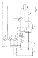
On a représenté à la
Cette unité de mesure de déphasage 43 comporte un générateur 431 d'un signal sinusoïdal à une fréquence de référence fref qui est, par exemple, égale à la fréquence nominale f0 du système de transmission ou à une fréquence voisine de cette fréquence nominale f0. Pour ce faire, le générateur 431 peut être synchronisé avec l'unité d'émission/réception 11 (synchronisation symbolisée par la flèche A), plus particulièrement avec le générateur interne (non représenté) de cette unité d'émission/réception 11 qui sert à la modulation du signal délivré par elle sur sa sortie Su ou à la démodulation du signal présent sur cette borne Su. Elle comporte également un générateur 432 d'un signal périodique, par exemple de forme sinusoïdale, à fréquence fb relativement plus basse que la fréquence de référence fref. On considérera par la suite, pour des raisons de simplification de raisonnement, que ces signaux sont sinusoïdaux.This phase-shifting
Elle comporte encore un modulateur 433 qui reçoit sur ses deux entrées les signaux sinusoïdaux respectivement générés par les générateurs 431 et 432 et qui délivre un signal sinusoïdal à une fréquence de mesure fm qui est soit la somme, soit la différence de la fréquence de référence fref et de la fréquence fb, signal entaché d'une certaine phase dont l'expression sera donnée par la suite. Le modulateur 433 peut être réalisé (voir
On a représenté à la 
que le signal Sref issu du générateur 431 s'exprime sous la forme : ![]()
![]()
that the signal S ref from the ![]()
![]()
On notera que si le sommateur 62 est remplacé par une unité effectuant la différence entre les signaux présents sur ses entrées respectives, le signal de mesure sm alors délivré par le modulateur 433 s'exprime, au signe près, sous la forme : ![]()
![]()
Sur la
Dans un premier mode de réalisation représenté à la
Dans le cas où le signal de mesure sm a pour fréquence la somme des fréquences fref et fb, le filtre 71 sera un filtre passe-bas pour ne laisser passer que la fréquence différence, soit la fréquence (fref + fb) - fref = fb. Dans le cas contraire où le signal de mesure sm a pour fréquence la différence des fréquences fref et fb, le filtre 71 sera un filtre passe-haut pour ne laisser passer que la fréquence somme, soit la fréquence fref - (fref - fb) = fb. On constate que, dans ces deux cas, le signal à la sortie de l'unité de détection 434 a une fréquence égale à la fréquence fb du générateur 432. Un autre mode de réalisation de l'unité de détection 434 est représenté à laIn the case where the measurement signal sm frequency is the sum of the frequencies f ref and f b , the
Dans le cas où le signal de mesure sm a pour fréquence la somme des fréquences fref et fb, le signal Sb issu du générateur 432 s'exprime sous la forme : ![]()
le signal SBc présente sur la borne commune Bc s'exprime sous la forme : ![]()
![]()
![]()
the signal S Bc present on the common terminal Bc is expressed in the form: ![]()
![]()
On notera que, pour ce faire, l'unité 82 devra être une unité de différence.Note that, to do this, the
Dans le cas contraire où le signal de mesure sm a pour fréquence la différence des fréquences fref et fb, l'unité 82 devra être un sommateur. En effet, on a alors : ![]()
![]()
![]()
![]()
On pourrait montrer que les signaux délivrés par l'unité de détection 434 dans son mode de réalisation de la
A la
Selon un mode de réalisation représenté à la
Le signal Sb issu du générateur 432 s'exprime sous la forme : ![]()

![]()
Alors le signal de sortie Sϕ du comparateur de phase 435 s'exprime sous la forme : ![]()
![]()
On constate qu'il est directement fonction de la phase (ϕ1 qu'a subi le signal de mesure sm dans le circuit résonnant 32.It can be seen that it is directly a function of the phase (φ1 that the measurement signal sm has undergone in the
Un autre mode de réalisation, connu en soi, d'un comparateur de phase 435 qui peut être utilisé en tant que comparateur de phase 435 est représenté à la
Si l'on revient sur la
La sortie de l'unité de mesure de déphasage 43 (par conséquence de l'unité d'asservissement 436) agit sur le circuit résonnant 32. De manière avantageuse, elle agit sur la valeur de la capacité 322 qui est donc variable et commandée.The output of the phase shift measuring unit 43 (as a consequence of the servo unit 436) acts on the
Dans un mode de réalisation représenté à la
On a représenté à la
Les capacités 325 et 326 sont avantageusement des capacités variables et commandées. Chacune d'elles peut être constituée de plusieurs capacités qui peuvent être, de manière commutable, mises en parallèle l'une avec au moins une autre, à l'instar de ce qui est montré à la
On a représenté à la
Afin de réduire le niveau de perturbation que peut engendrer la mesure du déphasage, le générateur 432 de l'unité de mesure de déphasage 43 n'est plus un générateur de signaux sinusoïdaux, mais un générateur de séquence pseudo-aléatoire. Un tel générateur de séquence pseudo-aléatoire utilise par exemple un polynôme générateur primitif modulo 2. Si la séquence est longue, l'écart type est grand et le signal produit par un tel générateur peut s'apparenter à un bruit blanc. Néanmoins, dans le choix de la longueur de la séquence, on tiendra compte aussi du fait qu'une séquence longue implique un étalement du spectre émis par le dispositif d'émission, ce qu'il est préférable d'éviter.In order to reduce the level of disturbance that may be caused by the measurement of the phase shift, the
On a représenté à la ![]()
![]()
Une telle séquence a une période de 215 - 1 temps d'horloge.Such a sequence has a period of 2-15 - 1 clock time.
On pourrait également choisir une séquence dont le polynôme générateur serait : ![]()
![]()
On notera que la phase du signal de mesure sm, après traversée du circuit résonnant 32, n'est plus constante mais qu'elle est également étalée dans le temps, d'une part, par le produit de convolution avec la séquence pseudo-aléatoire et, d'autre part, par la fonction de transfert du circuit résonnant 32. La phase est évaluée par des moments statistiques, principalement la moyenne.It will be noted that the phase of the measurement signal sm, after passing through the
Claims (22)
- Method for tuning the resonant frequency of a resonant circuit (12; 22; 32) comprising at least one adaptive tuning means (322) and an inductive element (121; 221; 321; 324) serving as an antenna of a transmission/reception device (10, 20) of a near-field transmission system on the transmission/reception frequency of said transmission/reception device (10, 20), characterized in that it comprises the following steps:- a step of receiving a modulated signal,- a step of measuring the phase shift (E10) of a signal generated in said inductive element upon reception of the modulated signal in said resonant circuit (12; 22; 32), and- a step (E20) of modifying the resonant frequency of said resonant circuit (12; 22; 32) when said phase shift measured in this manner is not null, so as to cancel said phase shift.
- Method of tuning according to claim 1 further comprising the following steps:- a step of measuring the phase shift (E10) of a signal to be transmitted, and- a step (E20) of modifying the resonant frequency of said resonant circuit (12; 22; 32) when said phase shift measured in this manner is not null, so as to cancel said phase shift.
- Method of tuning according to claim 1 or 2 wherein the step of measuring said phase shift (E10) comprises the following steps:- a step (E11) of generating a measurement signal, the frequency of which is equal to the nominal frequency of said transmission system or to a frequency in the neighborhood of said nominal frequency,- a step (E12) of injecting said measurement signal to the input of said resonant circuit,- a step (E13) of retrieving said measurement signal at the output of said resonant circuit,- a step (E14) of measuring the phase shift between the retrieved signal and said measurement signal,- a step of controlling said resonant circuit as a function of the result of the step (E14) of measuring the phase shift.
- Transmission/reception device (10, 20) of a near-field transmission system, said transmission/reception device comprising a transmission/reception unit (31) connected to a resonant circuit (12; 22; 32) comprising at least one adaptive tuning means (322) and an inductive element (121; 221; 321; 324) serving as an antenna to said transmission/reception device, characterized in that said transmission/reception device (10, 20) further comprises a phase shift measuring means (33; 43) for measuring a phase shift of a signal generated in said inductive element upon reception of a modulated signal in said resonant circuit (12; 22; 32), and for delivering a control signal to said resonant circuit (12; 22; 32) for modifying its resonant frequency, wherein said control signal tends to cancel said phase shift.
- Transmission/reception device of a near-field transmission system according to claim 4, wherein said phase shift measuring means (33; 43) further measures a phase shift of a signal to be transmitted, and said transmission/reception device (10, 20) is configured for delivering a control signal to said resonant circuit (12; 22; 32) for modifying its resonant frequency, wherein said control signal tends to cancel said phase shift.
- Transmission/reception device of a near-field transmission system according to claim 4 or 5, wherein said phase shift measuring means (33; 43) is provided for:- generating a measurement signal having a frequency equal to the nominal frequency of said transmission system or to a frequency in the neighborhood of said nominal frequency,- injecting said measurement signal to the input of said resonant circuit,- retrieving said measurement signal at the output of said resonant circuit,- measuring the phase shift between the retrieved signal and said measurement signal, and- controlling said means that said resonant circuit comprises for modifying its resonant frequency, so as to cancel the phase shift measured in this manner.
- Transmission/reception device of a near-field transmission system according to claim 6, wherein said phase shift measuring means (33; 43) comprises, for generating said measurement signal:- a first generator (431), the transmission frequency of which is equal to the nominal frequency of said transmission system or to a frequency in the neighborhood of said nominal frequency,- a second generator (432), the transmission frequency of which is essentially lower than that of the first generator (431),- a modulator (433) receiving at its inputs the signals generated by said first and second generators (431 and 432) and delivering as a measurement signal a signal, the transmission frequency of which is the sum or the difference of the transmission frequencies of said generators (431 and 432).
- Transmission/reception device of a near-field transmission system according to claim 7, wherein said modulator (433) consists of a multiplier (50) receiving at its inputs the signals generated by said first and second generators (431 and 432), a filter (51), the input of which is connected to the output of said multiplier (50), said filter (51) being provided for filtering one of the side bands of the signal at the output of said multiplier (50) and for passing the other side band, wherein the measurement signal is the output signal of said filter (51).
- Transmission/reception device of a near-field transmission system according to claim 7, wherein said modulator (433) consists of a first and second multiplier (60a and 60b), as well as a first and second π/2 phase-shifter (61a and 61b), wherein said first multiplier (60a) receives at one input the signal generated by said first generator (431) and, at the other input, the signal generated by said second generator (432) after phase-shifting in said second phase-shifter (61b), and said second multiplier (60b) receives at one input the signal generated by said second generator (432) and, at the other input, the signal generated by said first generator (431) after phase-shifting in said first phase-shifter (61a), wherein the output of each multiplier (60a, 60b) is connected to the input of an adder (62) or to a unit making the difference, the output of which delivering said measurement signal.
- Transmission/reception device of a near-field transmission system according to one of claims 7 to 9, wherein said phase shift measuring means comprises, for measuring the phase shift between said measurement signal and said measurement signal after passing through the resonant circuit:- a detection unit (434) receiving at an input the measurement signal after passing in said resonant circuit (12; 22; 32) and, at the other input, the signal generated by said second generator (431) and delivering, at its output, a signal at the transmission frequency of said second generator (432) and having a phase that is a linear function of the phase shift undergone by said measurement signal in said resonant circuit, and- a phase comparator (435) receiving at an input the signal delivered by said detection unit (434) and, on the other input, the signal generated by said first generator (432) and delivering at its output said control signal that is a function of said phase shift.
- Transmission/reception device of a near-field transmission system according to claim 10, wherein said detection unit (434) consists of a multiplier (70) receiving at its inputs the measurement signal after passing through said resonant circuit (12; 22; 32) and the signal generated by said second generator (431), and a filter (71), the input of which is connected to the output of said multiplier (70), said filter (71) being provided for filtering one of the side bands of the output signal of said multiplier (70) and for passing the other side band.
- Transmission/reception device of a near-field transmission system according to claim 10, wherein said detection unit (434) consists of a first and second multiplier (80a and 80b), as well as a first and second π/2 phase-shifter (91a and 91b), wherein said first multiplier (80a) receives at one input the measurement signal after passing through said resonant circuit (12; 22; 32) and, at the other input, the signal generated by said second generator (431) after phase shifting in said second phase-shifter (81b) and said second multiplier (80b) receives at one input the signal generated by said second generator (431) and, at the other input, the signal measured after passing through said resonant circuit (12; 22; 32) after phase shifting in said first phase-shifter (81a), the output of each multiplier (80a; 80b) being connected to the input of an adder (82) or a unit making the difference.
- Transmission/reception device of a near-field transmission system according to one of claims 6 to 12, wherein said phase shift measuring means (43) comprises, for controlling said means that said resonant circuit (12; 22; 32) comprises for modifying its resonant frequency, a controlling unit (436) which receives at its input the phase shift signal and delivers a polarization signal of said control means of said resonant circuit (12; 22; 32), the amplitude of which is such that said measured phase shift is null.
- Transmission/reception device of a near-field transmission system according to one of claims 4 to 13, wherein said resonant circuit (12; 22; 32) comprises an inductor that is coupled in parallel with a capacitor, said inductor serving as an antenna to said transmission/reception device.
- Transmission/reception device of a near-field transmission system according to one of claims 4 to 13, wherein said resonant circuit comprises a transformer with symmetrical windings (324), said windings being coupled in parallel to those capacitors having the same value, wherein said transformer serves as an antenna to said transmission/reception device.
- Transmission/reception device of a near-field transmission system according to claim 14 or 15, wherein said capacitor or each capacitor is a variable controlled capacitor.
- Transmission/reception device of a near-field transmission system according to claim 16, wherein said capacitor or each capacitor consists of several capacitors (C1 to Cn), wherein one of which can be put in parallel with at least one other, in a commutable manner or using commuting elements (2001 to 200n).
- Transmission/reception device of a near-field transmission system according to claim 17, wherein each commuting element is driven by one of the output bits of an analog/digital converter (200) receiving the phase shift signal delivered by said phase shift measuring means (43).
- Transmission/reception device of a near-field transmission system according to one of claims 7 to 18, wherein said first generator (431) is a generator of sinusoidal signals.
- Transmission/reception device of a near-field transmission system according to one of claims 7 to 19, wherein said second generator (432) is a generator of sinusoidal signals.
- Transmission/reception device of a near-field transmission system according to one of claims 7 to 19, wherein said second generator is a generator of pseudo-random sequences.
- Transmission/reception device of a near-field transmission system according to claim 21, wherein said generator of pseudo-random sequences uses a modulo 2 primitive generating polynom for transmitting said sequences.
Applications Claiming Priority (1)
| Application Number | Priority Date | Filing Date | Title |
|---|---|---|---|
| FR0704523A FR2917924B1 (en) | 2007-06-25 | 2007-06-25 | METHOD OF ANTENNA RESONANCE FREQUENCY ACCORDING |
Publications (2)
| Publication Number | Publication Date |
|---|---|
| EP2009790A1 EP2009790A1 (en) | 2008-12-31 |
| EP2009790B1 true EP2009790B1 (en) | 2012-08-01 |
Family
ID=38984478
Family Applications (1)
| Application Number | Title | Priority Date | Filing Date |
|---|---|---|---|
| EP08158734A Active EP2009790B1 (en) | 2007-06-25 | 2008-06-23 | Method for tuning the resonant frequency of an antenna |
Country Status (2)
| Country | Link |
|---|---|
| EP (1) | EP2009790B1 (en) |
| FR (1) | FR2917924B1 (en) |
Families Citing this family (1)
| Publication number | Priority date | Publication date | Assignee | Title |
|---|---|---|---|---|
| FR3026209B1 (en) * | 2014-09-22 | 2016-11-11 | St Microelectronics Int Nv | METHOD FOR NON-CONTACT COMMUNICATION BETWEEN TWO NFC DEVICES WITH REDUCTION OF IMPACT OF EXTERNAL NOISE TRANSMISSION |
Family Cites Families (2)
| Publication number | Priority date | Publication date | Assignee | Title |
|---|---|---|---|---|
| JPH11215111A (en) * | 1998-01-26 | 1999-08-06 | Mitsubishi Electric Corp | Radio terminal equipment |
| GB0505060D0 (en) * | 2005-03-11 | 2005-04-20 | Innovision Res & Tech Plc | Gain controlled impedance |
-
2007
- 2007-06-25 FR FR0704523A patent/FR2917924B1/en active Active
-
2008
- 2008-06-23 EP EP08158734A patent/EP2009790B1/en active Active
Also Published As
| Publication number | Publication date |
|---|---|
| EP2009790A1 (en) | 2008-12-31 |
| FR2917924A1 (en) | 2008-12-26 |
| FR2917924B1 (en) | 2009-12-04 |
Similar Documents
| Publication | Publication Date | Title |
|---|---|---|
| EP2469783B1 (en) | FSK radio signal receiver with high-sensitivity demodulator and method for operating said receiver | |
| EP3156810B1 (en) | Measurement of shielding attenuation | |
| FR2946464A1 (en) | CONTACTLESS DATA TRANSMISSION | |
| EP3561730B1 (en) | Method for adjusting the phase of the signal emitted by an object capable of contactless communication with a reader by active load modulation, and corresponding object | |
| FR2770700A1 (en) | DEVICE AND METHOD FOR SYNCHRONIZING OSCILLATORS IN A DATA COMMUNICATION SYSTEM | |
| EP0709959B1 (en) | Correction of a frequency offset | |
| EP2705468A1 (en) | Method and device for modulating the amplitude of an electromagnetic signal transmitted by a wireless transceiver | |
| EP1369813B1 (en) | Reader for electromagnetic transponder | |
| EP0647031A1 (en) | Circuit for correcting phase-shift and amplitudes | |
| EP0113611B1 (en) | Device for the automatic linearisation of the frequency-control signal characteristic of a frequency-modulated oscillator with variable frequency | |
| EP3242146B1 (en) | Method and system for communicating high-sensitivity signals with synchronous demodulation | |
| EP2009790B1 (en) | Method for tuning the resonant frequency of an antenna | |
| FR2765052A1 (en) | POLARIZED CODE DIFFERENCE MULTIPLE ACCESS SIGNAL TRANSMISSION AND RECEPTION SYSTEM | |
| EP0541406A1 (en) | Procedure and device for the transmission of two informations in a spread spectrum link | |
| EP0951147B1 (en) | Receiver and a method for tuning one of the radio frequency stages in a receiver | |
| EP0792027A1 (en) | Multi-band radio-telephone apparatus | |
| EP0274958B1 (en) | Device for compensating the doppler effect produced by the relative motion between receiver and transmitter, tuned at the same frequency, in a radioreceiver | |
| FR2884983A1 (en) | BROADBAND DEPHASING DEVICE | |
| FR2460050A1 (en) | DIGITAL DATA HYPERFREQUENCY TRANSMISSION SYSTEM | |
| FR2811495A1 (en) | METHOD AND DIPOSITIVE FOR PROTECTING A TRANSMISSION CHANNEL BETWEEN A BASE UNIT AND A MOBILE UNIT | |
| EP1759327B1 (en) | Contactless, synchronous phase demodulation method, and associated reader | |
| FR3056831B1 (en) | ANTENNA WITH FERROMAGNETIC RODS FITTED AND COUPLED BETWEEN THEM | |
| FR2554992A1 (en) | DEVICE FOR COMPENSATING THE SENSITIVITY TO ACCELERATION OF AN OSCILLATOR | |
| FR3042663B1 (en) | SETTING THE REINJECTION OF A TRANSMIT SIGNAL IN A RECEIVING CHAIN OF AN ON-LINE CURRENT DATA TRANSMISSION EQUIPMENT | |
| EP0293287B1 (en) | Spread spectrum phase demodulator test system |
Legal Events
| Date | Code | Title | Description |
|---|---|---|---|
| PUAI | Public reference made under article 153(3) epc to a published international application that has entered the european phase |
Free format text: ORIGINAL CODE: 0009012 |
|
| AK | Designated contracting states |
Kind code of ref document: A1 Designated state(s): AT BE BG CH CY CZ DE DK EE ES FI FR GB GR HR HU IE IS IT LI LT LU LV MC MT NL NO PL PT RO SE SI SK TR |
|
| AX | Request for extension of the european patent |
Extension state: AL BA MK RS |
|
| RAP1 | Party data changed (applicant data changed or rights of an application transferred) |
Owner name: SAGEM MOBILES |
|
| 17P | Request for examination filed |
Effective date: 20090311 |
|
| AKX | Designation fees paid |
Designated state(s): AT BE BG CH CY CZ DE DK EE ES FI FR GB GR HR HU IE IS IT LI LT LU LV MC MT NL NO PL PT RO SE SI SK TR |
|
| 17Q | First examination report despatched |
Effective date: 20101103 |
|
| RAP1 | Party data changed (applicant data changed or rights of an application transferred) |
Owner name: APPLE INC. |
|
| GRAP | Despatch of communication of intention to grant a patent |
Free format text: ORIGINAL CODE: EPIDOSNIGR1 |
|
| GRAS | Grant fee paid |
Free format text: ORIGINAL CODE: EPIDOSNIGR3 |
|
| GRAA | (expected) grant |
Free format text: ORIGINAL CODE: 0009210 |
|
| AK | Designated contracting states |
Kind code of ref document: B1 Designated state(s): AT BE BG CH CY CZ DE DK EE ES FI FR GB GR HR HU IE IS IT LI LT LU LV MC MT NL NO PL PT RO SE SI SK TR |
|
| REG | Reference to a national code |
Ref country code: GB Ref legal event code: FG4D Free format text: NOT ENGLISH |
|
| REG | Reference to a national code |
Ref country code: CH Ref legal event code: EP Ref country code: AT Ref legal event code: REF Ref document number: 569112 Country of ref document: AT Kind code of ref document: T Effective date: 20120815 |
|
| REG | Reference to a national code |
Ref country code: IE Ref legal event code: FG4D Free format text: LANGUAGE OF EP DOCUMENT: FRENCH |
|
| REG | Reference to a national code |
Ref country code: DE Ref legal event code: R096 Ref document number: 602008017528 Country of ref document: DE Effective date: 20120927 |
|
| REG | Reference to a national code |
Ref country code: NL Ref legal event code: T3 |
|
| REG | Reference to a national code |
Ref country code: AT Ref legal event code: MK05 Ref document number: 569112 Country of ref document: AT Kind code of ref document: T Effective date: 20120801 |
|
| REG | Reference to a national code |
Ref country code: LT Ref legal event code: MG4D Effective date: 20120801 |
|
| PG25 | Lapsed in a contracting state [announced via postgrant information from national office to epo] |
Ref country code: HR Free format text: LAPSE BECAUSE OF FAILURE TO SUBMIT A TRANSLATION OF THE DESCRIPTION OR TO PAY THE FEE WITHIN THE PRESCRIBED TIME-LIMIT Effective date: 20120801 Ref country code: AT Free format text: LAPSE BECAUSE OF FAILURE TO SUBMIT A TRANSLATION OF THE DESCRIPTION OR TO PAY THE FEE WITHIN THE PRESCRIBED TIME-LIMIT Effective date: 20120801 Ref country code: LT Free format text: LAPSE BECAUSE OF FAILURE TO SUBMIT A TRANSLATION OF THE DESCRIPTION OR TO PAY THE FEE WITHIN THE PRESCRIBED TIME-LIMIT Effective date: 20120801 Ref country code: IS Free format text: LAPSE BECAUSE OF FAILURE TO SUBMIT A TRANSLATION OF THE DESCRIPTION OR TO PAY THE FEE WITHIN THE PRESCRIBED TIME-LIMIT Effective date: 20121201 Ref country code: NO Free format text: LAPSE BECAUSE OF FAILURE TO SUBMIT A TRANSLATION OF THE DESCRIPTION OR TO PAY THE FEE WITHIN THE PRESCRIBED TIME-LIMIT Effective date: 20121101 Ref country code: FI Free format text: LAPSE BECAUSE OF FAILURE TO SUBMIT A TRANSLATION OF THE DESCRIPTION OR TO PAY THE FEE WITHIN THE PRESCRIBED TIME-LIMIT Effective date: 20120801 Ref country code: CY Free format text: LAPSE BECAUSE OF FAILURE TO SUBMIT A TRANSLATION OF THE DESCRIPTION OR TO PAY THE FEE WITHIN THE PRESCRIBED TIME-LIMIT Effective date: 20120801 |
|
| PG25 | Lapsed in a contracting state [announced via postgrant information from national office to epo] |
Ref country code: SE Free format text: LAPSE BECAUSE OF FAILURE TO SUBMIT A TRANSLATION OF THE DESCRIPTION OR TO PAY THE FEE WITHIN THE PRESCRIBED TIME-LIMIT Effective date: 20120801 Ref country code: GR Free format text: LAPSE BECAUSE OF FAILURE TO SUBMIT A TRANSLATION OF THE DESCRIPTION OR TO PAY THE FEE WITHIN THE PRESCRIBED TIME-LIMIT Effective date: 20121102 Ref country code: SI Free format text: LAPSE BECAUSE OF FAILURE TO SUBMIT A TRANSLATION OF THE DESCRIPTION OR TO PAY THE FEE WITHIN THE PRESCRIBED TIME-LIMIT Effective date: 20120801 Ref country code: PL Free format text: LAPSE BECAUSE OF FAILURE TO SUBMIT A TRANSLATION OF THE DESCRIPTION OR TO PAY THE FEE WITHIN THE PRESCRIBED TIME-LIMIT Effective date: 20120801 Ref country code: LV Free format text: LAPSE BECAUSE OF FAILURE TO SUBMIT A TRANSLATION OF THE DESCRIPTION OR TO PAY THE FEE WITHIN THE PRESCRIBED TIME-LIMIT Effective date: 20120801 Ref country code: PT Free format text: LAPSE BECAUSE OF FAILURE TO SUBMIT A TRANSLATION OF THE DESCRIPTION OR TO PAY THE FEE WITHIN THE PRESCRIBED TIME-LIMIT Effective date: 20121203 |
|
| PG25 | Lapsed in a contracting state [announced via postgrant information from national office to epo] |
Ref country code: DK Free format text: LAPSE BECAUSE OF FAILURE TO SUBMIT A TRANSLATION OF THE DESCRIPTION OR TO PAY THE FEE WITHIN THE PRESCRIBED TIME-LIMIT Effective date: 20120801 Ref country code: ES Free format text: LAPSE BECAUSE OF FAILURE TO SUBMIT A TRANSLATION OF THE DESCRIPTION OR TO PAY THE FEE WITHIN THE PRESCRIBED TIME-LIMIT Effective date: 20121112 Ref country code: RO Free format text: LAPSE BECAUSE OF FAILURE TO SUBMIT A TRANSLATION OF THE DESCRIPTION OR TO PAY THE FEE WITHIN THE PRESCRIBED TIME-LIMIT Effective date: 20120801 Ref country code: CZ Free format text: LAPSE BECAUSE OF FAILURE TO SUBMIT A TRANSLATION OF THE DESCRIPTION OR TO PAY THE FEE WITHIN THE PRESCRIBED TIME-LIMIT Effective date: 20120801 Ref country code: EE Free format text: LAPSE BECAUSE OF FAILURE TO SUBMIT A TRANSLATION OF THE DESCRIPTION OR TO PAY THE FEE WITHIN THE PRESCRIBED TIME-LIMIT Effective date: 20120801 |
|
| PG25 | Lapsed in a contracting state [announced via postgrant information from national office to epo] |
Ref country code: SK Free format text: LAPSE BECAUSE OF FAILURE TO SUBMIT A TRANSLATION OF THE DESCRIPTION OR TO PAY THE FEE WITHIN THE PRESCRIBED TIME-LIMIT Effective date: 20120801 |
|
| PLBE | No opposition filed within time limit |
Free format text: ORIGINAL CODE: 0009261 |
|
| STAA | Information on the status of an ep patent application or granted ep patent |
Free format text: STATUS: NO OPPOSITION FILED WITHIN TIME LIMIT |
|
| 26N | No opposition filed |
Effective date: 20130503 |
|
| PG25 | Lapsed in a contracting state [announced via postgrant information from national office to epo] |
Ref country code: BG Free format text: LAPSE BECAUSE OF FAILURE TO SUBMIT A TRANSLATION OF THE DESCRIPTION OR TO PAY THE FEE WITHIN THE PRESCRIBED TIME-LIMIT Effective date: 20121101 |
|
| REG | Reference to a national code |
Ref country code: DE Ref legal event code: R097 Ref document number: 602008017528 Country of ref document: DE Effective date: 20130503 |
|
| BERE | Be: lapsed |
Owner name: APPLE INC. Effective date: 20130630 |
|
| PG25 | Lapsed in a contracting state [announced via postgrant information from national office to epo] |
Ref country code: MC Free format text: LAPSE BECAUSE OF FAILURE TO SUBMIT A TRANSLATION OF THE DESCRIPTION OR TO PAY THE FEE WITHIN THE PRESCRIBED TIME-LIMIT Effective date: 20120801 |
|
| REG | Reference to a national code |
Ref country code: CH Ref legal event code: PL |
|
| REG | Reference to a national code |
Ref country code: IE Ref legal event code: MM4A |
|
| PG25 | Lapsed in a contracting state [announced via postgrant information from national office to epo] |
Ref country code: BE Free format text: LAPSE BECAUSE OF NON-PAYMENT OF DUE FEES Effective date: 20130630 |
|
| PG25 | Lapsed in a contracting state [announced via postgrant information from national office to epo] |
Ref country code: LI Free format text: LAPSE BECAUSE OF NON-PAYMENT OF DUE FEES Effective date: 20130630 Ref country code: IE Free format text: LAPSE BECAUSE OF NON-PAYMENT OF DUE FEES Effective date: 20130623 Ref country code: CH Free format text: LAPSE BECAUSE OF NON-PAYMENT OF DUE FEES Effective date: 20130630 |
|
| PG25 | Lapsed in a contracting state [announced via postgrant information from national office to epo] |
Ref country code: MT Free format text: LAPSE BECAUSE OF FAILURE TO SUBMIT A TRANSLATION OF THE DESCRIPTION OR TO PAY THE FEE WITHIN THE PRESCRIBED TIME-LIMIT Effective date: 20120801 |
|
| PG25 | Lapsed in a contracting state [announced via postgrant information from national office to epo] |
Ref country code: TR Free format text: LAPSE BECAUSE OF FAILURE TO SUBMIT A TRANSLATION OF THE DESCRIPTION OR TO PAY THE FEE WITHIN THE PRESCRIBED TIME-LIMIT Effective date: 20120801 |
|
| PG25 | Lapsed in a contracting state [announced via postgrant information from national office to epo] |
Ref country code: LU Free format text: LAPSE BECAUSE OF NON-PAYMENT OF DUE FEES Effective date: 20130623 Ref country code: HU Free format text: LAPSE BECAUSE OF FAILURE TO SUBMIT A TRANSLATION OF THE DESCRIPTION OR TO PAY THE FEE WITHIN THE PRESCRIBED TIME-LIMIT; INVALID AB INITIO Effective date: 20080623 |
|
| REG | Reference to a national code |
Ref country code: FR Ref legal event code: PLFP Year of fee payment: 9 |
|
| REG | Reference to a national code |
Ref country code: FR Ref legal event code: PLFP Year of fee payment: 10 |
|
| REG | Reference to a national code |
Ref country code: FR Ref legal event code: PLFP Year of fee payment: 11 |
|
| P01 | Opt-out of the competence of the unified patent court (upc) registered |
Effective date: 20230523 |
|
| PGFP | Annual fee paid to national office [announced via postgrant information from national office to epo] |
Ref country code: NL Payment date: 20230515 Year of fee payment: 16 Ref country code: IT Payment date: 20230510 Year of fee payment: 16 Ref country code: FR Payment date: 20230510 Year of fee payment: 16 Ref country code: DE Payment date: 20230425 Year of fee payment: 16 |
|
| PGFP | Annual fee paid to national office [announced via postgrant information from national office to epo] |
Ref country code: GB Payment date: 20230504 Year of fee payment: 16 |