EP0949516B1 - Elektrooptisches Verfahren zur Signalverarbeitung, Vorrichtung zur Durchführung des Verfahrens und Anwendung - Google Patents
Elektrooptisches Verfahren zur Signalverarbeitung, Vorrichtung zur Durchführung des Verfahrens und Anwendung Download PDFInfo
- Publication number
- EP0949516B1 EP0949516B1 EP99400852A EP99400852A EP0949516B1 EP 0949516 B1 EP0949516 B1 EP 0949516B1 EP 99400852 A EP99400852 A EP 99400852A EP 99400852 A EP99400852 A EP 99400852A EP 0949516 B1 EP0949516 B1 EP 0949516B1
- Authority
- EP
- European Patent Office
- Prior art keywords
- layer
- guiding layer
- wavelength
- guiding
- optical radiation
- Prior art date
- Legal status (The legal status is an assumption and is not a legal conclusion. Google has not performed a legal analysis and makes no representation as to the accuracy of the status listed.)
- Expired - Lifetime
Links
- 238000000034 method Methods 0.000 title claims description 11
- 230000003287 optical effect Effects 0.000 claims description 26
- 229910021420 polycrystalline silicon Inorganic materials 0.000 claims description 23
- 229920005591 polysilicon Polymers 0.000 claims description 23
- VYPSYNLAJGMNEJ-UHFFFAOYSA-N Silicium dioxide Chemical compound O=[Si]=O VYPSYNLAJGMNEJ-UHFFFAOYSA-N 0.000 claims description 20
- 230000005855 radiation Effects 0.000 claims description 20
- 238000010521 absorption reaction Methods 0.000 claims description 19
- 239000000758 substrate Substances 0.000 claims description 12
- 239000004065 semiconductor Substances 0.000 claims description 10
- 230000000694 effects Effects 0.000 claims description 7
- 230000008878 coupling Effects 0.000 claims description 5
- 238000010168 coupling process Methods 0.000 claims description 5
- 238000005859 coupling reaction Methods 0.000 claims description 5
- 229910052814 silicon oxide Inorganic materials 0.000 claims description 4
- 239000000969 carrier Substances 0.000 claims description 3
- 229910052581 Si3N4 Inorganic materials 0.000 claims 2
- HQVNEWCFYHHQES-UHFFFAOYSA-N silicon nitride Chemical compound N12[Si]34N5[Si]62N3[Si]51N64 HQVNEWCFYHHQES-UHFFFAOYSA-N 0.000 claims 2
- 229910052681 coesite Inorganic materials 0.000 description 8
- 229910052906 cristobalite Inorganic materials 0.000 description 8
- 239000000377 silicon dioxide Substances 0.000 description 8
- 235000012239 silicon dioxide Nutrition 0.000 description 8
- 229910052682 stishovite Inorganic materials 0.000 description 8
- 229910052905 tridymite Inorganic materials 0.000 description 8
- XUIMIQQOPSSXEZ-UHFFFAOYSA-N Silicon Chemical compound [Si] XUIMIQQOPSSXEZ-UHFFFAOYSA-N 0.000 description 7
- 238000005516 engineering process Methods 0.000 description 6
- 229910052710 silicon Inorganic materials 0.000 description 5
- 239000010703 silicon Substances 0.000 description 5
- 239000000463 material Substances 0.000 description 4
- 230000005693 optoelectronics Effects 0.000 description 4
- 239000007787 solid Substances 0.000 description 4
- 239000010408 film Substances 0.000 description 3
- 229910004298 SiO 2 Inorganic materials 0.000 description 2
- 150000004767 nitrides Chemical class 0.000 description 2
- 101100536354 Drosophila melanogaster tant gene Proteins 0.000 description 1
- 229910000577 Silicon-germanium Inorganic materials 0.000 description 1
- 230000009471 action Effects 0.000 description 1
- 229910021417 amorphous silicon Inorganic materials 0.000 description 1
- 230000008859 change Effects 0.000 description 1
- 239000013078 crystal Substances 0.000 description 1
- 238000010292 electrical insulation Methods 0.000 description 1
- 238000002474 experimental method Methods 0.000 description 1
- 238000009432 framing Methods 0.000 description 1
- 229910052732 germanium Inorganic materials 0.000 description 1
- GNPVGFCGXDBREM-UHFFFAOYSA-N germanium atom Chemical compound [Ge] GNPVGFCGXDBREM-UHFFFAOYSA-N 0.000 description 1
- 239000011810 insulating material Substances 0.000 description 1
- 239000012212 insulator Substances 0.000 description 1
- 238000004519 manufacturing process Methods 0.000 description 1
- 239000002184 metal Substances 0.000 description 1
- 239000000203 mixture Substances 0.000 description 1
- 230000004048 modification Effects 0.000 description 1
- 238000012986 modification Methods 0.000 description 1
- 230000003647 oxidation Effects 0.000 description 1
- 238000007254 oxidation reaction Methods 0.000 description 1
- 239000004038 photonic crystal Substances 0.000 description 1
- 238000001020 plasma etching Methods 0.000 description 1
- 230000000644 propagated effect Effects 0.000 description 1
- 230000000717 retained effect Effects 0.000 description 1
- 239000010409 thin film Substances 0.000 description 1
- 230000001960 triggered effect Effects 0.000 description 1
Images

Classifications
-
- G—PHYSICS
- G02—OPTICS
- G02B—OPTICAL ELEMENTS, SYSTEMS OR APPARATUS
- G02B6/00—Light guides; Structural details of arrangements comprising light guides and other optical elements, e.g. couplings
- G02B6/24—Coupling light guides
- G02B6/42—Coupling light guides with opto-electronic elements
- G02B6/43—Arrangements comprising a plurality of opto-electronic elements and associated optical interconnections
-
- G—PHYSICS
- G02—OPTICS
- G02B—OPTICAL ELEMENTS, SYSTEMS OR APPARATUS
- G02B6/00—Light guides; Structural details of arrangements comprising light guides and other optical elements, e.g. couplings
- G02B6/10—Light guides; Structural details of arrangements comprising light guides and other optical elements, e.g. couplings of the optical waveguide type
- G02B6/12—Light guides; Structural details of arrangements comprising light guides and other optical elements, e.g. couplings of the optical waveguide type of the integrated circuit kind
- G02B6/12004—Combinations of two or more optical elements
-
- G—PHYSICS
- G02—OPTICS
- G02B—OPTICAL ELEMENTS, SYSTEMS OR APPARATUS
- G02B6/00—Light guides; Structural details of arrangements comprising light guides and other optical elements, e.g. couplings
- G02B6/24—Coupling light guides
- G02B6/26—Optical coupling means
-
- G—PHYSICS
- G02—OPTICS
- G02B—OPTICAL ELEMENTS, SYSTEMS OR APPARATUS
- G02B6/00—Light guides; Structural details of arrangements comprising light guides and other optical elements, e.g. couplings
- G02B6/24—Coupling light guides
- G02B6/42—Coupling light guides with opto-electronic elements
- G02B6/4295—Coupling light guides with opto-electronic elements coupling with semiconductor devices activated by light through the light guide, e.g. thyristors, phototransistors
Definitions
- the present invention relates to the field of optoelectronics.
- the document US Patent 5,625,729 discloses an optoelectronic device for coupling between an external optical wave and a local optical wave.
- the local optical wave is supported by a plurality of electrodes and a structure associated with the electrodes.
- the electrodes are spaced apart in a substantially regular array and are adapted for two functions. First, the electrodes perform a resonant coupling between the external wave and the local wave. Secondly the electrodes allow a potential difference between the adjacent electrodes.
- the present invention based on the result of experiments aims to provide new means with improved performance compared to prior known systems.
- a main object of the present invention is in particular to propose means which make it possible to optimize the coupling of an optical beam on a semiconductor structure, without requiring the use of semiconducting compositions or of a delicate technology to be used. implemented.
- said assembly superimposed on the substrate comprises the guiding layer and at least one layer interposed between the substrate and this guiding layer and which has a refractive index lower than that of the guiding layer, to the length of the applied optical radiation.
- the present invention makes it possible in particular to ensure very fast interconnections between electronic components while ensuring perfect electrical insulation between them.
- the present invention also relates to a device for implementing this method.
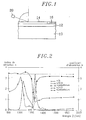
- an optoelectronic device comprising a substrate 10 of semiconductor material, for example based on silicon, and superposed thereon, successively a first layer 12 of a semi-insulating material, for example silicon oxide SiO 2 and a second layer 14 forming a guiding layer, for example polysilicon.
- a guiding layer for example polysilicon.
- Semiconductor oxide formed in the extension of the guiding layer 14.
- the inventor has determined that for a conventional MOS technology structure, comprising a polysilicon guiding layer 14 deposited for example by CVD on an underlying layer 12 of silicon oxide, preferably the radiation applied by the means 20 on the guiding layer 14, has a wavelength of the order of 8 .mu.m under an incidence A of between 70 and 76 °.
- the inventor has indeed determined that under these conditions the radiation is guided in the polysilicon layer 14. With this incidence, the wave penetrates into the guiding layer at an angle of about 16 ° which is the critical angle of propagation in guided mode in the polysilicon. On the other hand, outside this parameter range, the light is not guided.
- the polysilicon layer 14 forming a guiding layer preferably has a thickness of the order of 200 to 400 nm, while the underlying oxide layer 12 has a thickness of at least 10 nm.
- the present invention thus makes it possible to effectively guide a monochromatic infrared wave in a polysilicon film obtained with conventional technology.
- the present invention can find many applications.
- the tripped transistor receives an optical control command signal from the triggering transistor via the guiding layer mentioned above.
- This application allows for example to use two transistors at different voltages or located in different circuit blocks.
- the state of the transistor can be modified by light at the appropriate wavelengths and by attacking the surface at a given angle.
- the transmitted light in addition to modifying the state of the transistor, can also be guided in the layer of gate material and act on one (or more) other transistor (s) without there being electrical contact between transistors (which is impossible to achieve in conventional architectures of known devices).
- the inventor has further determined that the guiding effect used in the context of the present invention is due to a resonant optical interference linked to the evanescent wave that exists at the two interfaces of the polysilicon layer.
- This resonant evanescent wave propagates longitudinally in the polysilicon layer.
- the guiding layer 14 is sandwiched between two framing layers (the layer 12 and the air or another layer similar to layer 12) having refractive indices lower than that of the guiding layer 14.
- the present invention thus makes it possible to obtain the conditions suitable for ensuring confinement of the light in the guiding layer 14, without requiring guiding layers of large thickness.
- the present invention makes it possible, in particular, a perfect compatibility between the planar technology of a MOS transistor and the technology for producing the guiding layer 14.
- the present invention makes it possible in particular to eliminate the differences in level existing in certain systems proposed in FIG. state of the art between the guiding layers and the semiconductor structures.
- the present invention can be applied to semiconductor structures, in particular based on polysilicon, whatever the crystalline state thereof: amorphous, microcrystalline or mono-crystalline (case of silicon on insulator).
- the present invention can also be applied to structures based on germanium.
- the technology of the layer 12 underlying the guiding layer 14 may be the subject of numerous variants. It may be for example a layer of oyde obtained by oxidation in dry phase (under O2) or wet (O2 + H2) or by CVD assisted or non-plasma or UV.
- the wavelength retained is preferably of the order of 9 .mu.m.
- the present invention may for example also find application in filters or photonic materials.
- a transistor which, depending on the incidence of attack of an associated guiding layer and the associated wavelength, will or will not be triggered.
- the present invention can find application in systems adapted to ensure the triggering of a transistor only after combination of two or more wavelengths, which allows an optical control logic (the combination of the wavelengths which attack the structure) with electrical effect (modification of the electrical state of the gate, so the transistor with or without guidance for action on another transistor).
- the present invention may also find application in the manufacture of photonic crystals by plasma etching of resonant structures which depend on the wavelength of the propagated light and the pitch of the grating.
- the guiding layer 14 directly receives the radiation on its surface.
- this guiding layer 14 it is conceivable to attack this guiding layer 14 at the end, or at the level of a window formed in a superimposed confinement layer, for example a layer similar to the underlying layer 12.
- the figure 2 reveals an absorption peak in the polysilicon guide layer 14 for E of the order of 1260 cm -1.
- the figure 3 represents similar curves for a structure in which the SiO2 layer is replaced by a Si3N4 nitride layer deposited on a silicon substrate.
- the figure 3 reveals an absorption peak in the polysilicon guiding layer 14 for E of the order of 1130 cm -1.
- the electrodes on a zone of the doping polysilicon guiding layer 14 to create a photo-modulation effect linked to the presence of free carriers present in the doped polysilicon layer.
- An electrical modulation induces an index modulation by the effect of the free carriers. And this effect is all the stronger as the wavelength range is close to the associated plasmon frequency.
- zones with high doping level positioned on the guiding portion 14, allows the creation of a resonant cavity that is easily associated with a cascade-type SiGe laser that is tuned to this wavelength.
Landscapes
- Physics & Mathematics (AREA)
- General Physics & Mathematics (AREA)
- Optics & Photonics (AREA)
- Engineering & Computer Science (AREA)
- Microelectronics & Electronic Packaging (AREA)
- Optical Integrated Circuits (AREA)
- Light Receiving Elements (AREA)
- Optical Couplings Of Light Guides (AREA)
Claims (11)
- Optisches Kopplungsverfahren in einem Wellenleiter, die Schritte umfassend, die darin bestehen:- Bereitstellung mindestens eines Halbleiter-Bauteils, das mindestens von einem Substrat (10) und einem überlagerten Ensemble gebildet wird, das mindestens eine Führungsschicht (14) umfasst, und wobei die Führungsschicht (14) aus Polysilizium ist und auf einer darunter liegenden Schicht (12) aus Siliziumoxid abgelagert, wobei die Führungsschicht (14) eine Dicke in der Größenordnung von 200 bis 400 nm hat, währenddessen die darunter liegende Schicht (12) eine Dicke von mindestens gleich 10 nm hat,- Ausüben auf die Führungsschicht (14) einer optischen Strahlung mit einer Wellenlänge in der Größenordnung von 8 µm unter einem Einfall (A) zwischen 70 und 76° inklusive, so dass das Ensemble bei dieser Wellenlänge und diesem Einfall einen spezifischen Absorptionspeak aufweist, der geeignet ist, die Führung der optischen Strahlung in der Führungsschicht (14) zu erlauben.
- Optisches Kopplungsverfahren in einem Wellenleiter, die Schritte umfassend, die darin bestehen:- Bereitstellung mindestens eines Halbleiter-Bauteils, das mindestens von einem Substrat (10) und einem überlagerten Ensemble gebildet wird, das mindestens eine Führungsschicht (14) umfasst, und wobei die Führungsschicht (14) aus Polysilizium ist und auf einer darunter liegenden Schicht (12) aus Siliziumnitrid abgelagert, wobei die Führungsschicht (14) eine Dicke in der Größenordnung von 200 bis 400 nm hat, währenddessen die darunter liegende Schicht (12) eine Dicke von mindestens gleich 10 nm hat,- Ausüben auf die Führungsschicht (14) einer optischen Strahlung mit einer Wellenlänge in der Größenordnung von 9 µm unter einem Einfall (A) zwischen 70 und 76° inklusive, so dass das Ensemble bei dieser Wellenlänge und diesem Einfall einen spezifischen Absorptionspeak aufweist, der geeignet ist, die Führung der optischen Strahlung in der Führungsschicht (14) zu erlauben.
- Verfahren nach einem der Ansprüche 1 oder 2, dadurch gekennzeichnet, dass das dem Substrat (10) überlagerte Ensemble (12, 14) die Führungsschicht (14) und mindestens eine zwischen dem Substrat (10) und dieser Führungsschicht (14) zwischengelagerte Schicht (12) umfasst und das einen Brechungskoeffizienten aufweist, der kleiner ist als der der Führungsschicht (14), bei der Wellenlänge der ausgeübten optischen Strahlung.
- Verfahren nach einem der Ansprüche 1 bis 3, dadurch gekennzeichnet, dass die Führungsschicht (14) einen hohen Koeffizienten n besitzt, in typischer Weise in der Größenordnung von 3 bis 4.
- Verfahren nach einem der Ansprüche 1 bis 4, dadurch gekennzeichnet, dass die Wellenlänge ω der optischen Strahlung, ausgedrückt in cm-1, inbegriffen ist zwischen der transversalen Frequenz ωT und der Längsfrequenz ωLO der unter der Führungsschicht (14) liegenden Schicht (12), das heißt ε1 (ω) <O und ωT < ω < ωLO.
- Vorrichtung zur Umsetzung des Verfahrens gemäß einem der Ansprüche 1 bis 5, umfassend:- mindestens ein Halbleiter-Bauteil, das mindestens von einem Substrat (10) und einem überlagerten Ensemble gebildet wird, das mindestens eine Führungsschicht (14) umfasst, und wobei die Führungsschicht (14) aus Polysilizium ist und auf einer darunter liegenden Schicht (12) aus Siliziumoxid abgelagert, wobei die Führungsschicht (14) eine Dicke in der Größenordnung von 200 bis 400 nm hat, währenddessen die darunter liegende Schicht (12) eine Dicke von mindestens gleich 10 nm hat, und- Mittel, die imstande sind, auf die Führungsschicht (14) eine optische Strahlung mit einer Wellenlänge in der Größenordnung von 8 µm unter einem Einfall (A) zwischen 70 und 76° inklusive auszuüben, so dass das Ensemble bei dieser Wellenlänge und diesem Einfall einen spezifischen Absorptionspeak aufweist, der geeignet ist, die Führung der optischen Strahlung in der Führungsschicht (14) zu erlauben.
- Vorrichtung zur Umsetzung des Verfahrens gemäß einem der Ansprüche 1 bis 5, umfassend,- mindestens ein Halbleiter-Bauteil, das mindestens von einem Substrat (10) und einem überlagerten Ensemble gebildet wird, das mindestens eine Führungsschicht (14) umfasst, und wobei die Führungsschicht (14) aus Polysilizium ist und auf einer darunter liegenden Schicht (12) aus Siliziumnitrid abgelagert, wobei die Führungsschicht (14) eine Dicke in der Größenordnung von 200 bis 400 nm hat, währenddessen die darunter liegende Schicht (12) eine Dicke von mindestens gleich 10 nm hat, und- Mittel, die imstande sind, auf die Führungsschicht (14) eine optische Strahlung mit einer Wellenlänge in der Größenordnung von 9 µm unter einem Einfall (A) zwischen 70 und 76° inklusive auszuüben, so dass das Ensemble bei dieser Wellenlänge und diesem Einfall einen spezifischen Absorptionspeak aufweist, der geeignet ist, die Führung der optischen Strahlung in der Führungsschicht (14) zu erlauben.
- Vorrichtung nach einem der Ansprüche 6 oder 7, dadurch gekennzeichnet, dass das dem Substrat (10) überlagerte Ensemble (12, 14) die Führungsschicht (14) und mindestens eine zwischen dem Substrat (10) und dieser Führungsschicht (14) zwischengelagerte Schicht (12) umfasst und das einen Brechungskoeffizienten aufweist, der kleiner ist als der der Führungsschicht (14), bei der Wellenlänge der ausgeübten optischen Strahlung.
- Vorrichtung nach einem der Ansprüche 6 bis 8, dadurch gekennzeichnet, dass die Führungsschicht (14) einen hohen Koeffizienten n besitzt, in typischer Weise in der Größenordnung von 3 bis 4.
- Vorrichtung nach einem der Ansprüche 6 bis 9, dadurch gekennzeichnet, dass die Wellenlänge ω der optischen Strahlung, ausgedrückt in cm-1, inbegriffen ist zwischen der transversalen Frequenz ωT und der Längsfrequenz ωLO der unter der Führungsschicht (14) liegenden Schicht (12), das heißt ε1 (ω)<O und ωT < ω < ωLO.
- Vorrichtung nach einem der Ansprüche 6 bis 10, dadurch gekennzeichnet, dass sie in einem Bereich der Führungsschicht (14) aufgebrachte Elektroden umfasst, um einen Effekt der Fotomodulation hervorzurufen, die an das Vorkommen freier Träger gebunden ist, die in der Führungsschicht vorhanden sind.
Applications Claiming Priority (2)
| Application Number | Priority Date | Filing Date | Title |
|---|---|---|---|
| FR9804557A FR2777358B1 (fr) | 1998-04-10 | 1998-04-10 | Procede electrooptique de traitement de signaux, dispositif pour la mise en oeuvre de celui-ci et utilisation |
| FR9804557 | 1998-04-10 |
Publications (2)
| Publication Number | Publication Date |
|---|---|
| EP0949516A1 EP0949516A1 (de) | 1999-10-13 |
| EP0949516B1 true EP0949516B1 (de) | 2008-07-16 |
Family
ID=9525149
Family Applications (1)
| Application Number | Title | Priority Date | Filing Date |
|---|---|---|---|
| EP99400852A Expired - Lifetime EP0949516B1 (de) | 1998-04-10 | 1999-04-08 | Elektrooptisches Verfahren zur Signalverarbeitung, Vorrichtung zur Durchführung des Verfahrens und Anwendung |
Country Status (5)
| Country | Link |
|---|---|
| US (1) | US6233380B1 (de) |
| EP (1) | EP0949516B1 (de) |
| JP (1) | JP5145614B2 (de) |
| DE (1) | DE69939083D1 (de) |
| FR (1) | FR2777358B1 (de) |
Families Citing this family (14)
| Publication number | Priority date | Publication date | Assignee | Title |
|---|---|---|---|---|
| US6602765B2 (en) * | 2000-06-12 | 2003-08-05 | Seiko Epson Corporation | Fabrication method of thin-film semiconductor device |
| US6920290B2 (en) * | 2001-07-11 | 2005-07-19 | Lockheed Martin Corporation | Multi-wavelength high bandwidth communication receiver and system |
| US20030123827A1 (en) * | 2001-12-28 | 2003-07-03 | Xtalight, Inc. | Systems and methods of manufacturing integrated photonic circuit devices |
| US6876784B2 (en) * | 2002-05-30 | 2005-04-05 | Nanoopto Corporation | Optical polarization beam combiner/splitter |
| US7386205B2 (en) * | 2002-06-17 | 2008-06-10 | Jian Wang | Optical device and method for making same |
| US7283571B2 (en) * | 2002-06-17 | 2007-10-16 | Jian Wang | Method and system for performing wavelength locking of an optical transmission source |
| US20040047039A1 (en) * | 2002-06-17 | 2004-03-11 | Jian Wang | Wide angle optical device and method for making same |
| CN100346196C (zh) | 2002-06-18 | 2007-10-31 | 纳诺普托公司 | 展现增强的功能性的光学组件及其制造方法 |
| CN1692291A (zh) | 2002-08-01 | 2005-11-02 | 纳诺普托公司 | 精密相位延迟装置和其制造方法 |
| US7013064B2 (en) * | 2002-10-09 | 2006-03-14 | Nanoopto Corporation | Freespace tunable optoelectronic device and method |
| US6920272B2 (en) * | 2002-10-09 | 2005-07-19 | Nanoopto Corporation | Monolithic tunable lasers and reflectors |
| EP1597616A4 (de) * | 2003-02-10 | 2008-04-09 | Nanoopto Corp | Universeller breitbandpolarisator, vorrichtungen damit und herstellungsverfahren dafür |
| US20040258355A1 (en) * | 2003-06-17 | 2004-12-23 | Jian Wang | Micro-structure induced birefringent waveguiding devices and methods of making same |
| US7597702B2 (en) * | 2003-09-17 | 2009-10-06 | Boston Scientific Scimed, Inc. | Balloon assembly with a torque |
Family Cites Families (16)
| Publication number | Priority date | Publication date | Assignee | Title |
|---|---|---|---|---|
| US3753157A (en) * | 1971-06-30 | 1973-08-14 | Ibm | Leaky wave couplers for guided elastic wave and guided optical wave devices |
| JPS5975656A (ja) * | 1982-10-25 | 1984-04-28 | Agency Of Ind Science & Technol | 半導体集積回路構造 |
| US4583818A (en) * | 1983-08-08 | 1986-04-22 | Gte Laboratories Incorporated | Optical device with surface plasmons |
| JPS60243606A (ja) * | 1984-05-17 | 1985-12-03 | Canon Inc | 薄膜型光学素子 |
| FR2588093B1 (fr) * | 1985-09-27 | 1987-11-20 | Thomson Csf | Polariseur par absorption differentielle, son procede de realisation et dispositif mettant en oeuvre ledit procede |
| JPS6371636A (ja) * | 1986-09-16 | 1988-04-01 | Matsushita Electronics Corp | シリコン中の不純物濃度の測定方法 |
| US4932743A (en) * | 1988-04-18 | 1990-06-12 | Ricoh Company, Ltd. | Optical waveguide device |
| US4915482A (en) * | 1988-10-27 | 1990-04-10 | International Business Machines Corporation | Optical modulator |
| DE3914377A1 (de) * | 1989-04-29 | 1990-11-08 | Basf Ag | Verfahren zur optischen filterung von polarisiertem licht |
| JPH04219657A (ja) * | 1990-04-13 | 1992-08-10 | Ricoh Co Ltd | 光磁気情報記録再生装置及びモードスプリッタ |
| US5321498A (en) * | 1991-12-28 | 1994-06-14 | Electronics & Telecommunications Research Institute | Planar integrated crossover optical system |
| JPH06151809A (ja) * | 1992-10-30 | 1994-05-31 | Toshiba Corp | 半導体装置 |
| US5625729A (en) * | 1994-08-12 | 1997-04-29 | Brown; Thomas G. | Optoelectronic device for coupling between an external optical wave and a local optical wave for optical modulators and detectors |
| US5502787A (en) * | 1995-05-22 | 1996-03-26 | At&T Corp. | Article comprising a semiconductor waveguide structure |
| JP3098173B2 (ja) * | 1995-06-09 | 2000-10-16 | シャープ株式会社 | 光カプラー及びその製造方法 |
| US5682455A (en) * | 1996-02-29 | 1997-10-28 | Northern Telecom Limited | Semiconductor optical waveguide |
-
1998
- 1998-04-10 FR FR9804557A patent/FR2777358B1/fr not_active Expired - Fee Related
-
1999
- 1999-04-08 DE DE69939083T patent/DE69939083D1/de not_active Expired - Lifetime
- 1999-04-08 EP EP99400852A patent/EP0949516B1/de not_active Expired - Lifetime
- 1999-04-12 US US09/289,667 patent/US6233380B1/en not_active Expired - Fee Related
- 1999-04-12 JP JP10436599A patent/JP5145614B2/ja not_active Expired - Fee Related
Non-Patent Citations (1)
| Title |
|---|
| A. BORGHESI ET AL.: "Influence of roughness and grain dimension on the optical functions of polycrystalline silicon films", THIN SOLID FILMS, no. 313-314, February 1998 (1998-02-01), pages 243 - 247, XP004132992 * |
Also Published As
| Publication number | Publication date |
|---|---|
| FR2777358B1 (fr) | 2000-06-30 |
| EP0949516A1 (de) | 1999-10-13 |
| FR2777358A1 (fr) | 1999-10-15 |
| JPH11330503A (ja) | 1999-11-30 |
| US6233380B1 (en) | 2001-05-15 |
| JP5145614B2 (ja) | 2013-02-20 |
| DE69939083D1 (de) | 2008-08-28 |
Similar Documents
| Publication | Publication Date | Title |
|---|---|---|
| JP2677353B2 (ja) | 光導波路 | |
| US7190524B2 (en) | Process for fabrication of high reflectors by reversal of layer sequence and application thereof | |
| EP0461991B1 (de) | Integriertes optisches Monomode-Raumfilter und Verfahren zu seiner Herstellung | |
| EP0949516A1 (de) | Elektrooptisches Verfahren zur Signalverarbeitung, Vorrichtung zur Durchführung des Verfahrens und Anwendung | |
| EP0240400B1 (de) | Optischer Wellenleiter aus Halbleitermaterial, Anwendung dieses Wellenleiters in einem Laser und Verfahren zu dessen Verwirklichung | |
| FR3051561B1 (fr) | Dispositif photonique integre a couplage optique ameliore | |
| EP1909080A1 (de) | Ultrasensibler optischer Detektor mit hoher zeitlicher Auflösung basierend auf einem Gitter. | |
| EP0219401A1 (de) | Differentieller Absorptionspolarisator, Verfahren und Vorrichtung für seine Herstellung | |
| EP3190672A1 (de) | Laserquelle mit halbleiter | |
| WO2019002763A1 (fr) | Source laser à semi-conducteur | |
| EP0539298A1 (de) | Integrierter elektro-optischer Modulator und dessen Herstellungsverfahren | |
| FR2953607A1 (fr) | Dispositif de couplage d'une onde electromagnetique entre un guide d'onde et un guide metallique a fente, procede de fabrication dudit dispositif | |
| EP0783118A1 (de) | Wellenlängendemultiplexer | |
| Taylor et al. | An integrated, crystalline organic waveguide-coupled InGaAs photodetector | |
| FR3052562B1 (fr) | Dispositif optique | |
| EP3314319B1 (de) | Optischer leiter | |
| EP4034922B1 (de) | Bragg-spiegel und verfahren zum produzieren eines bragg-spiegels | |
| EP3599501A1 (de) | Athermischer modulator-umschalter mit zwei übereinander angeordneten ringen | |
| EP4614200A1 (de) | Optischer koppler mit polarisationstrennung | |
| FR3148651A1 (fr) | Dispositif optoelectronique de deformation a la demande d’une portion cristalline semiconductrice couplee optiquement a un guide d’onde | |
| FR2598263A1 (fr) | Laser semiconducteur a haut niveau de non-linearite et procede de passivation differentielle des faces clivees de ce laser. | |
| EP0198735A1 (de) | Optoelektronischer Wandler und Verfahren zu seiner Herstellung | |
| WO1999024853A1 (fr) | Dispositif optique a guide d'ondes pour le transfert d'energie electromagnetique sous forme d'un faisceau de rayonnement |
Legal Events
| Date | Code | Title | Description |
|---|---|---|---|
| PUAI | Public reference made under article 153(3) epc to a published international application that has entered the european phase |
Free format text: ORIGINAL CODE: 0009012 |
|
| AK | Designated contracting states |
Kind code of ref document: A1 Designated state(s): DE FR GB NL |
|
| AX | Request for extension of the european patent |
Free format text: AL;LT;LV;MK;RO;SI |
|
| 17P | Request for examination filed |
Effective date: 20000306 |
|
| AKX | Designation fees paid |
Free format text: DE FR GB NL |
|
| RAP1 | Party data changed (applicant data changed or rights of an application transferred) |
Owner name: FAHRENHEIT THERMOSCOPE LLC |
|
| GRAP | Despatch of communication of intention to grant a patent |
Free format text: ORIGINAL CODE: EPIDOSNIGR1 |
|
| GRAS | Grant fee paid |
Free format text: ORIGINAL CODE: EPIDOSNIGR3 |
|
| GRAA | (expected) grant |
Free format text: ORIGINAL CODE: 0009210 |
|
| AK | Designated contracting states |
Kind code of ref document: B1 Designated state(s): DE FR GB NL |
|
| REG | Reference to a national code |
Ref country code: GB Ref legal event code: FG4D Free format text: NOT ENGLISH |
|
| REF | Corresponds to: |
Ref document number: 69939083 Country of ref document: DE Date of ref document: 20080828 Kind code of ref document: P |
|
| NLV1 | Nl: lapsed or annulled due to failure to fulfill the requirements of art. 29p and 29m of the patents act | ||
| PG25 | Lapsed in a contracting state [announced via postgrant information from national office to epo] |
Ref country code: NL Free format text: LAPSE BECAUSE OF FAILURE TO SUBMIT A TRANSLATION OF THE DESCRIPTION OR TO PAY THE FEE WITHIN THE PRESCRIBED TIME-LIMIT Effective date: 20080716 |
|
| PLBE | No opposition filed within time limit |
Free format text: ORIGINAL CODE: 0009261 |
|
| STAA | Information on the status of an ep patent application or granted ep patent |
Free format text: STATUS: NO OPPOSITION FILED WITHIN TIME LIMIT |
|
| 26N | No opposition filed |
Effective date: 20090417 |
|
| PGFP | Annual fee paid to national office [announced via postgrant information from national office to epo] |
Ref country code: GB Payment date: 20120327 Year of fee payment: 14 |
|
| PGFP | Annual fee paid to national office [announced via postgrant information from national office to epo] |
Ref country code: DE Payment date: 20120430 Year of fee payment: 14 |
|
| PGFP | Annual fee paid to national office [announced via postgrant information from national office to epo] |
Ref country code: FR Payment date: 20120503 Year of fee payment: 14 |
|
| GBPC | Gb: european patent ceased through non-payment of renewal fee |
Effective date: 20130408 |
|
| PG25 | Lapsed in a contracting state [announced via postgrant information from national office to epo] |
Ref country code: GB Free format text: LAPSE BECAUSE OF NON-PAYMENT OF DUE FEES Effective date: 20130408 Ref country code: DE Free format text: LAPSE BECAUSE OF NON-PAYMENT OF DUE FEES Effective date: 20131101 |
|
| REG | Reference to a national code |
Ref country code: FR Ref legal event code: ST Effective date: 20131231 |
|
| PG25 | Lapsed in a contracting state [announced via postgrant information from national office to epo] |
Ref country code: FR Free format text: LAPSE BECAUSE OF NON-PAYMENT OF DUE FEES Effective date: 20130430 |
|
| REG | Reference to a national code |
Ref country code: DE Ref legal event code: R119 Ref document number: 69939083 Country of ref document: DE Effective date: 20131101 |