EP0240400B1 - Optischer Wellenleiter aus Halbleitermaterial, Anwendung dieses Wellenleiters in einem Laser und Verfahren zu dessen Verwirklichung - Google Patents
Optischer Wellenleiter aus Halbleitermaterial, Anwendung dieses Wellenleiters in einem Laser und Verfahren zu dessen Verwirklichung Download PDFInfo
- Publication number
- EP0240400B1 EP0240400B1 EP87400622A EP87400622A EP0240400B1 EP 0240400 B1 EP0240400 B1 EP 0240400B1 EP 87400622 A EP87400622 A EP 87400622A EP 87400622 A EP87400622 A EP 87400622A EP 0240400 B1 EP0240400 B1 EP 0240400B1
- Authority
- EP
- European Patent Office
- Prior art keywords
- layer
- optical waveguide
- waveguide
- optical
- chemical attack
- Prior art date
- Legal status (The legal status is an assumption and is not a legal conclusion. Google has not performed a legal analysis and makes no representation as to the accuracy of the status listed.)
- Expired - Lifetime
Links
- 230000003287 optical effect Effects 0.000 title claims abstract description 222
- 239000004065 semiconductor Substances 0.000 title claims abstract description 71
- 238000000034 method Methods 0.000 title claims description 42
- 239000000463 material Substances 0.000 claims abstract description 115
- 239000000126 substance Substances 0.000 claims abstract description 115
- 239000000203 mixture Substances 0.000 claims abstract description 5
- 239000000758 substrate Substances 0.000 claims description 18
- 238000004519 manufacturing process Methods 0.000 claims description 15
- 230000008569 process Effects 0.000 claims description 10
- 238000000407 epitaxy Methods 0.000 claims description 8
- GPXJNWSHGFTCBW-UHFFFAOYSA-N Indium phosphide Chemical compound [In]#P GPXJNWSHGFTCBW-UHFFFAOYSA-N 0.000 claims description 7
- 238000000927 vapour-phase epitaxy Methods 0.000 claims description 5
- 230000009471 action Effects 0.000 claims description 3
- 238000005530 etching Methods 0.000 claims description 3
- 238000003486 chemical etching Methods 0.000 claims 5
- 229910000530 Gallium indium arsenide Inorganic materials 0.000 claims 2
- 230000001902 propagating effect Effects 0.000 claims 2
- 241000282320 Panthera leo Species 0.000 claims 1
- 238000010521 absorption reaction Methods 0.000 claims 1
- 239000012071 phase Substances 0.000 description 15
- 229910001218 Gallium arsenide Inorganic materials 0.000 description 8
- GYHNNYVSQQEPJS-UHFFFAOYSA-N Gallium Chemical compound [Ga] GYHNNYVSQQEPJS-UHFFFAOYSA-N 0.000 description 5
- 229910000673 Indium arsenide Inorganic materials 0.000 description 5
- 230000008901 benefit Effects 0.000 description 5
- RPQDHPTXJYYUPQ-UHFFFAOYSA-N indium arsenide Chemical compound [In]#[As] RPQDHPTXJYYUPQ-UHFFFAOYSA-N 0.000 description 5
- 229910052751 metal Inorganic materials 0.000 description 4
- 239000002184 metal Substances 0.000 description 4
- BASFCYQUMIYNBI-UHFFFAOYSA-N platinum Chemical compound [Pt] BASFCYQUMIYNBI-UHFFFAOYSA-N 0.000 description 4
- JBRZTFJDHDCESZ-UHFFFAOYSA-N AsGa Chemical compound [As]#[Ga] JBRZTFJDHDCESZ-UHFFFAOYSA-N 0.000 description 3
- 230000004888 barrier function Effects 0.000 description 3
- YFXPPSKYMBTNAV-UHFFFAOYSA-N bensultap Chemical compound C=1C=CC=CC=1S(=O)(=O)SCC(N(C)C)CSS(=O)(=O)C1=CC=CC=C1 YFXPPSKYMBTNAV-UHFFFAOYSA-N 0.000 description 3
- 238000005229 chemical vapour deposition Methods 0.000 description 3
- 238000000151 deposition Methods 0.000 description 3
- 230000005684 electric field Effects 0.000 description 3
- 229910052738 indium Inorganic materials 0.000 description 3
- APFVFJFRJDLVQX-UHFFFAOYSA-N indium atom Chemical compound [In] APFVFJFRJDLVQX-UHFFFAOYSA-N 0.000 description 3
- VYPSYNLAJGMNEJ-UHFFFAOYSA-N Silicium dioxide Chemical compound O=[Si]=O VYPSYNLAJGMNEJ-UHFFFAOYSA-N 0.000 description 2
- 230000005540 biological transmission Effects 0.000 description 2
- 230000008021 deposition Effects 0.000 description 2
- 238000009792 diffusion process Methods 0.000 description 2
- 230000000694 effects Effects 0.000 description 2
- PCHJSUWPFVWCPO-UHFFFAOYSA-N gold Chemical compound [Au] PCHJSUWPFVWCPO-UHFFFAOYSA-N 0.000 description 2
- 239000010931 gold Substances 0.000 description 2
- 229910052737 gold Inorganic materials 0.000 description 2
- 230000000873 masking effect Effects 0.000 description 2
- 238000001451 molecular beam epitaxy Methods 0.000 description 2
- 229910052697 platinum Inorganic materials 0.000 description 2
- 239000012808 vapor phase Substances 0.000 description 2
- WSMQKESQZFQMFW-UHFFFAOYSA-N 5-methyl-pyrazole-3-carboxylic acid Chemical compound CC1=CC(C(O)=O)=NN1 WSMQKESQZFQMFW-UHFFFAOYSA-N 0.000 description 1
- 230000002411 adverse Effects 0.000 description 1
- 239000000969 carrier Substances 0.000 description 1
- 239000013043 chemical agent Substances 0.000 description 1
- 239000002131 composite material Substances 0.000 description 1
- 150000001875 compounds Chemical class 0.000 description 1
- 230000008878 coupling Effects 0.000 description 1
- 238000010168 coupling process Methods 0.000 description 1
- 238000005859 coupling reaction Methods 0.000 description 1
- 238000010586 diagram Methods 0.000 description 1
- 239000006185 dispersion Substances 0.000 description 1
- 230000009977 dual effect Effects 0.000 description 1
- 238000005516 engineering process Methods 0.000 description 1
- 239000011521 glass Substances 0.000 description 1
- 230000010365 information processing Effects 0.000 description 1
- 230000010354 integration Effects 0.000 description 1
- 230000003993 interaction Effects 0.000 description 1
- 238000002955 isolation Methods 0.000 description 1
- GQYHUHYESMUTHG-UHFFFAOYSA-N lithium niobate Chemical compound [Li+].[O-][Nb](=O)=O GQYHUHYESMUTHG-UHFFFAOYSA-N 0.000 description 1
- 230000004807 localization Effects 0.000 description 1
- 238000003754 machining Methods 0.000 description 1
- 239000013307 optical fiber Substances 0.000 description 1
- 230000005693 optoelectronics Effects 0.000 description 1
- 125000002524 organometallic group Chemical group 0.000 description 1
- 230000000737 periodic effect Effects 0.000 description 1
- 230000010363 phase shift Effects 0.000 description 1
- 239000011347 resin Substances 0.000 description 1
- 229920005989 resin Polymers 0.000 description 1
- 239000000377 silicon dioxide Substances 0.000 description 1
- 238000005476 soldering Methods 0.000 description 1
- 230000003595 spectral effect Effects 0.000 description 1
Images




Classifications
-
- B—PERFORMING OPERATIONS; TRANSPORTING
- B82—NANOTECHNOLOGY
- B82Y—SPECIFIC USES OR APPLICATIONS OF NANOSTRUCTURES; MEASUREMENT OR ANALYSIS OF NANOSTRUCTURES; MANUFACTURE OR TREATMENT OF NANOSTRUCTURES
- B82Y20/00—Nanooptics, e.g. quantum optics or photonic crystals
-
- G—PHYSICS
- G02—OPTICS
- G02B—OPTICAL ELEMENTS, SYSTEMS OR APPARATUS
- G02B6/00—Light guides; Structural details of arrangements comprising light guides and other optical elements, e.g. couplings
- G02B6/10—Light guides; Structural details of arrangements comprising light guides and other optical elements, e.g. couplings of the optical waveguide type
- G02B6/12—Light guides; Structural details of arrangements comprising light guides and other optical elements, e.g. couplings of the optical waveguide type of the integrated circuit kind
- G02B6/122—Basic optical elements, e.g. light-guiding paths
-
- H—ELECTRICITY
- H01—ELECTRIC ELEMENTS
- H01S—DEVICES USING THE PROCESS OF LIGHT AMPLIFICATION BY STIMULATED EMISSION OF RADIATION [LASER] TO AMPLIFY OR GENERATE LIGHT; DEVICES USING STIMULATED EMISSION OF ELECTROMAGNETIC RADIATION IN WAVE RANGES OTHER THAN OPTICAL
- H01S5/00—Semiconductor lasers
- H01S5/20—Structure or shape of the semiconductor body to guide the optical wave ; Confining structures perpendicular to the optical axis, e.g. index or gain guiding, stripe geometry, broad area lasers, gain tailoring, transverse or lateral reflectors, special cladding structures, MQW barrier reflection layers
-
- H—ELECTRICITY
- H01—ELECTRIC ELEMENTS
- H01S—DEVICES USING THE PROCESS OF LIGHT AMPLIFICATION BY STIMULATED EMISSION OF RADIATION [LASER] TO AMPLIFY OR GENERATE LIGHT; DEVICES USING STIMULATED EMISSION OF ELECTROMAGNETIC RADIATION IN WAVE RANGES OTHER THAN OPTICAL
- H01S5/00—Semiconductor lasers
- H01S5/20—Structure or shape of the semiconductor body to guide the optical wave ; Confining structures perpendicular to the optical axis, e.g. index or gain guiding, stripe geometry, broad area lasers, gain tailoring, transverse or lateral reflectors, special cladding structures, MQW barrier reflection layers
- H01S5/22—Structure or shape of the semiconductor body to guide the optical wave ; Confining structures perpendicular to the optical axis, e.g. index or gain guiding, stripe geometry, broad area lasers, gain tailoring, transverse or lateral reflectors, special cladding structures, MQW barrier reflection layers having a ridge or stripe structure
- H01S5/227—Buried mesa structure ; Striped active layer
-
- H—ELECTRICITY
- H01—ELECTRIC ELEMENTS
- H01S—DEVICES USING THE PROCESS OF LIGHT AMPLIFICATION BY STIMULATED EMISSION OF RADIATION [LASER] TO AMPLIFY OR GENERATE LIGHT; DEVICES USING STIMULATED EMISSION OF ELECTROMAGNETIC RADIATION IN WAVE RANGES OTHER THAN OPTICAL
- H01S5/00—Semiconductor lasers
- H01S5/30—Structure or shape of the active region; Materials used for the active region
- H01S5/34—Structure or shape of the active region; Materials used for the active region comprising quantum well or superlattice structures, e.g. single quantum well [SQW] lasers, multiple quantum well [MQW] lasers or graded index separate confinement heterostructure [GRINSCH] lasers
-
- H—ELECTRICITY
- H10—SEMICONDUCTOR DEVICES; ELECTRIC SOLID-STATE DEVICES NOT OTHERWISE PROVIDED FOR
- H10H—INORGANIC LIGHT-EMITTING SEMICONDUCTOR DEVICES HAVING POTENTIAL BARRIERS
- H10H20/00—Individual inorganic light-emitting semiconductor devices having potential barriers, e.g. light-emitting diodes [LED]
- H10H20/01—Manufacture or treatment
- H10H20/011—Manufacture or treatment of bodies, e.g. forming semiconductor layers
- H10H20/013—Manufacture or treatment of bodies, e.g. forming semiconductor layers having light-emitting regions comprising only Group III-V materials
-
- H—ELECTRICITY
- H01—ELECTRIC ELEMENTS
- H01S—DEVICES USING THE PROCESS OF LIGHT AMPLIFICATION BY STIMULATED EMISSION OF RADIATION [LASER] TO AMPLIFY OR GENERATE LIGHT; DEVICES USING STIMULATED EMISSION OF ELECTROMAGNETIC RADIATION IN WAVE RANGES OTHER THAN OPTICAL
- H01S5/00—Semiconductor lasers
- H01S5/20—Structure or shape of the semiconductor body to guide the optical wave ; Confining structures perpendicular to the optical axis, e.g. index or gain guiding, stripe geometry, broad area lasers, gain tailoring, transverse or lateral reflectors, special cladding structures, MQW barrier reflection layers
- H01S5/2054—Methods of obtaining the confinement
- H01S5/2081—Methods of obtaining the confinement using special etching techniques
-
- H—ELECTRICITY
- H01—ELECTRIC ELEMENTS
- H01S—DEVICES USING THE PROCESS OF LIGHT AMPLIFICATION BY STIMULATED EMISSION OF RADIATION [LASER] TO AMPLIFY OR GENERATE LIGHT; DEVICES USING STIMULATED EMISSION OF ELECTROMAGNETIC RADIATION IN WAVE RANGES OTHER THAN OPTICAL
- H01S5/00—Semiconductor lasers
- H01S5/20—Structure or shape of the semiconductor body to guide the optical wave ; Confining structures perpendicular to the optical axis, e.g. index or gain guiding, stripe geometry, broad area lasers, gain tailoring, transverse or lateral reflectors, special cladding structures, MQW barrier reflection layers
- H01S5/22—Structure or shape of the semiconductor body to guide the optical wave ; Confining structures perpendicular to the optical axis, e.g. index or gain guiding, stripe geometry, broad area lasers, gain tailoring, transverse or lateral reflectors, special cladding structures, MQW barrier reflection layers having a ridge or stripe structure
- H01S5/227—Buried mesa structure ; Striped active layer
- H01S5/2275—Buried mesa structure ; Striped active layer mesa created by etching
-
- H—ELECTRICITY
- H01—ELECTRIC ELEMENTS
- H01S—DEVICES USING THE PROCESS OF LIGHT AMPLIFICATION BY STIMULATED EMISSION OF RADIATION [LASER] TO AMPLIFY OR GENERATE LIGHT; DEVICES USING STIMULATED EMISSION OF ELECTROMAGNETIC RADIATION IN WAVE RANGES OTHER THAN OPTICAL
- H01S5/00—Semiconductor lasers
- H01S5/30—Structure or shape of the active region; Materials used for the active region
- H01S5/32—Structure or shape of the active region; Materials used for the active region comprising PN junctions, e.g. hetero- or double- heterostructures
- H01S5/323—Structure or shape of the active region; Materials used for the active region comprising PN junctions, e.g. hetero- or double- heterostructures in AIIIBV compounds, e.g. AlGaAs-laser, InP-based laser
- H01S5/3235—Structure or shape of the active region; Materials used for the active region comprising PN junctions, e.g. hetero- or double- heterostructures in AIIIBV compounds, e.g. AlGaAs-laser, InP-based laser emitting light at a wavelength longer than 1000 nm, e.g. InP-based 1300 nm and 1500 nm lasers
- H01S5/32391—Structure or shape of the active region; Materials used for the active region comprising PN junctions, e.g. hetero- or double- heterostructures in AIIIBV compounds, e.g. AlGaAs-laser, InP-based laser emitting light at a wavelength longer than 1000 nm, e.g. InP-based 1300 nm and 1500 nm lasers based on In(Ga)(As)P
Definitions
- the present invention relates to an optical waveguide of semiconductor material, a laser applying this waveguide and a production method.
- the simplest structures which made it possible to obtain the first guides in semiconductor materials were formed by depositing a thin guide layer lightly doped on a substrate a few hundred microns thick considered to be infinite at infrared wavelengths used.
- a structure is represented in FIG. 3, with the guide layer referenced 1 and the substrate referenced 2.
- EP-A 0 002 827 constitutes an example of the state of the art.
- FIG. 4 This structure comprises a substrate 21 carrying an n-doped buffer layer (20), which carries an optical guide layer 1 supplemented by guide elements 10 and 11 doped respectively with n and p + , and which excited by an electric field applied to a metal electrode 12 allows phase modulation of a light wave by electrooptic effect.
- the substrate 21 and the buffer layer 20 can be made of indium phosphide (InP).
- the guiding layer and the guiding elements can be made of Gallium and Indium Arsenide (GainAs) or of Gallium and Indium Arsenide phosphide (Ga In As P).
- the upper confinement material of the structure consists of air, the effective index guidance is strong and this can be a problem if we want to make a directional coupler because we are then brought to bring the rib guides to distances sometimes less than a micron.
- To reduce guidance by effective index we can leave part of the upper buffer layer, but this is generally of the order of a micron of thickness and it is very technologically difficult to obtain surface states minimizing the diffusion losses.
- MOCVD vapor phase epitaxy method
- the invention relates to a guide structure which can be produced by the combination of the vapor phase epitaxy method and the selective chemical attack method.
- the vapor phase epitaxy process makes it possible to obtain ultra-thin layers making it possible to reduce guidance by effective index at will.
- the selective chemical attack process allows
- the structure then obtained is produced with great precision on the one hand in the thickness of the layers on the other hand in the geometry of these elements and it also makes it possible to obtain an excellent surface quality.
- the invention relates to an integrated optical waveguide of semiconductor material comprising at least one layer of an optical guide material of a first index covering at least one lower optical confinement layer, of a second index, at least one Ribbon-shaped optical guide element of determined width, extending above said optical guide layer in the direction of propagation of the guide, said guide tape having a fourth index and at least one upper optical confinement layer, d a third index, covering said guide tape while extending on either side thereof above said guide layer, the first index being greater than the second index and the third index and the fourth index being also greater than the third index, said waveguide being characterized in that it further comprises at least one chemical attack stop layer interposed between said co guide pole on the one hand, and said guide tape and said upper confinement layer on the other hand the assembly being arranged so that said guide tape rests on said chemical attack stop layer however said layer upper containment covers said tape as well as said barrier layer, the material of this chemical attack stop layer being of a chemical nature different from that of said ribbon and the thickness of this chemical attack stop layer being chosen low enough not to
- Waveguides produced in the form of ribs machined in a waveguide layer exist in the art and have been described previously with reference to FIGS. 1 to 4. However, these waveguides cannot be produced with precision and with the quality necessary to obtain a waveguide having sufficiently low propagation losses.
- the refractive index n1 of the optical guide layer 1 is greater than the refractive index n2 of the lower optical confinement layer 2. It is also higher than the index n3 of the upper optical confining layer 3. L the refractive index n5 of the guide element is greater than the index n3 of the upper optical confinement layer 3.
- the energy bandwidths E2 and E3 of the materials of the layers of lower and upper optical confinement are each greater than the energy bandwidth E1 of the optical guide layer 1 as well as the energy bandwidth E5 of the optical guide element.
- the chemical attack stop layer 4 is of a different chemical nature from the optical guide element 5 so that the latter can be attacked by chemical agents which do not attack the optical stop layer. chemical attack.
- the thickness of the chemical attack stop layer 4 has a negligible thickness compared to the operating wavelength of the waveguide, which wavelength is determined by the nature of the material constituting the guide layer optics 1.
- the thickness h4 of the chemical attack stop layer will be between one tenth and one hundredth of the wavelength of use. Under these conditions, the presence of the chemical attack stop layer does not significantly harm the optical qualities of the structure.
- Guidance by effective index in the structure of Figure 5 is very low, of the order of 10-4 for example.
- the optical guide element 5 can then have a width w greater than in the known techniques. The influence of the imperfections of the flanks of the element 5 and in particular the roughness of the flanks therefore loses importance, especially since the thickness of the optical guide element is small.
- the width w of the optical guide element 5 is therefore a function of its thickness and it takes a maximum value depending on whether the guide is single transverse mode or not. It is also possible with va their different from w to get, for example, a dual mode guide. Examples of numeric values will be given later.
- FIG. 6 represents in perspective the waveguide of FIG. 5 with the optical guide element 5 placed along a plane xOy.
- the lower optical confinement layer 2, the optical guide layer and the chemical attack stop layer 4 are parallel to the plane xOy and their dimensions in the directions in this plane are not necessarily limited.
- the guide element 5 has the form of a ribbon oriented along the Ox axis and allows light propagation along the Ox axis.
- the upper optical confinement layer 3 covers the chemical attack stop layer 4 and the element 5.
- the optical guide layer 1 is made of a material whose mesh parameter is adapted to a multiple or a submultiple of the lower optical confinement layer 2.
- the chemical attack stop layer 4 is made of material whose parameter mesh is suitable for a multiple or a sub-multiple of the guide layer 1.
- the mesh parameters of the upper optical confinement layer 3 and of the optical guide element 5 are adapted to one another and are adapted to that of the chemical attack stop layer 4.
- the materials used for a waveguide thus described can be produced for example using semiconductor compounds from groups III and V of the periodic table.
- the optical confinement layers 2 and 3 and the chemical attack stop layer can be an indium phosphide InP while the optical guide layer 1 and the guide element 5 can be made of Gallium Arsenide and indium (Ga ln As) or as phosphide of gallium arsenide and indium (Ga In As P).
- An optical guide made of gallium and indium arsenide phosphide operates at wavelengths of around 1.5 ⁇ m.
- the thickness (e4) of the chemical attack stop layer may advantageously be of the order of 100 Angstroms, which will allow it not to have an adverse effect on the transmission qualities of the waveguide.
- the structure of FIGS. 5 and 6 provides for doping for the lower optical confinement layer 2, a layer 21 doped n + and a layer 20 doped n- in contact with the layer of optical guidance 1.
- the layers 20 and 30 constitute buffer layers.
- the optical guide element 5 is produced differently. Indeed, it has several sub-layers.
- the chemical attack stop layer 4 it comprises a sublayer 5.1 of optical guide material, then a chemical attack stop sublayer 4.2. These sublayers are themselves covered by an alternation of sublayers of optical guide material 5.2 to 5.n and of chemical attack stop sublayers 4.3 to 4.n.
- These different sublayers are made of materials whose mesh parameter is adapted to the mesh parameters of the neighboring sublayers and, for the sublayers of ends 5.1 and 5.n, adapted to the material of the barrier layer d chemical attack 4 (for sublayer 5.1) and to the material of the upper optical confinement layer 3 (for sublayer 5.n).
- the refractive indices of the chemical attack stop sublayers 4.2 to 4.n and the refractive indices of the optical guide sublayers 5.1 to 5.n are such that effective index guidance is carried out in the structure shown in figure 8.
- the chemical attack stop sublayers 4.2 to 4.n may be made with the same material as the chemical attack stop layer 4.
- the underlayers optical guide 5.1 to 5.n could be the same as that used in the above description for the optical guide layer 5.
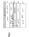
- This figure shows the lower optical confinement layers 20 and 21 respectively doped n- and n + , the optical guide layer 1, the chemical attack stop layer 4, the optical guide element 5 and the upper optical confinement layers 30 and 31 respectively n- and P + doped .
- a metal electrode 6 making it possible to apply an electric field and thus obtain a phase shift.
- This figure shows the lower optical confinement layers 20 and 21 respectively n + and n doped, the optical guide layer 1, the chemical attack stop layer 4, the optical guide element 5, and the p-doped upper optical confinement layer 3.
- a layer 32 of gallium and indium arsenide (Ga In As) serving as a contact layer and a metal electrode 6 allowing an electric field to be applied.
- the type of materials constituting the different layers and the thicknesses of these layers will determine the type of laser and in particular the operating wavelength of the laser.
- indium phosphide will be used for the layers 2, 4, 3 and for the optical guide layers 1.5
- gallium arsenide phosphide will be used and indium Ga In As P.
- indium phosphide will also be used for layers 2, 3, 4 and for phosphoric guide layers 1.5, phosphide d will be used. gallium and indium arsenide Ga In As P.
- This value of e1 will make it possible to have a single-mode guide in the direction Oz and a good localization of the electromagnetic wave in the optical guide layer 1.
- the width w will depend on the thickness e5.
- the waveguide of the invention and the semiconductor laser implementing this waveguide can give rise to different embodiments.
- this will thus increase the transmission power.
- a laser with coupled cavities in the same mode has thus been successfully produced.
- an optical guide layer 1 is produced on a lower optical confinement layer 2.
- the materials used for these two layers are adapted in mesh and the refractive index of layer 2 is less than l refractive index of layer 1.
- this production step may include the production on an n + doped substrate of an n- doped buffer layer.
- layer 1 by epitaxy in the vapor phase also called in English terminology MO CVD (Metalorganic Chemical Vapor Deposition) or by any other process such as molecular beam epitaxy (MBE).
- MO CVD Metalorganic Chemical Vapor Deposition
- MBE molecular beam epitaxy
- an optical attack stop layer 4 is produced on the optical guide layer 1. These two layers are also adapted in mesh.
- the refractive index of layer 4 is lower than that of layer 1.
- the thickness of this layer must be small compared to the wavelength of use of the waveguide and to have a uniform layer 4 , a method as mentioned previously will also be used for this step.
- the material used for layer 4 will be of a chemical nature. Different from that which will be used in the step which follows so as not to be attacked chemically in a subsequent step of chemical attack.
- a layer of an optical guide material 50 is produced.
- the material used will be adapted in mesh to that of layer 1.
- the invention provides an epitaxy which allows a uniform deposition and according to a thickness which can be determined with precision.
- a chemical attack is carried out on the layer 50 previously deposited so as to cut from this layer, one or more optical guide elements 5.
- the protection of the layer part (s) 50 which are to give rise to the optical guide element (s) 5 is done by any masking method known in the art.
- the chemical used for the chemical attack is chosen so as to attack the material of the layer 50 but not to attack the material of the chemical attack stop layer 4.
- the layer 50 having been perfectly calibrated in thickness and being relatively thin, an optical guide element 5 of uniform thickness is obtained, after chemical attack, the sides of which are cut out with sharpness.
- a structure is obtained as shown in FIG. 13.
- an upper optical confinement layer 3 is formed on the optical guide element 5 and the chemical attack stop layer 3.
- This layer can be made, as before, by epitaxy by making as shown in FIG. 14, a buffer layer 30 and a doped layer 31 (p + for example).
- the material used for the layers 30 and 31 is adapted in mesh to the element 5 and the barrier layer 4. Its refractive index is lower than that of the guide layer 1 and that of the element 5.
- the production of such an electrode is known in the art and the method of the invention has made it possible to produce a laser.
- the thickness of the different layers and the width of the optical guide element 5 will be chosen according to the materials used, as described above, to determine the optimal operating wavelength waveguide or laser produced.
- the third step previously described comprises several alternating phases for producing sublayers of guide material 5.1 to 5.n and for producing chemical attack stop sublayers 4.2 to 4.n.
- the fourth step also includes an alternating succession of chemical attack phases. These different phases use a single prior masking of the optical guide element to be produced.
- Each chemical attack phase will be carried out using a chemical which makes it possible to attack either an optical guide sublayer 5.1 to 5.n) or a chemical attack stop sublayer (4.2 to 4.n).
- the material used in the production phases of the underlays of guide material 5.1 to 5.n will be the same for all the underlays.
- the material used in the production phases of the chemical attack stop sublayers 4.2 to 4.n will be the same as that of layer 4 deposited during the second step.
- the guide elements can be wider and the influence of the roughness of the leading flanks on the losses, already reduced by the potential low height of the guide elements still loses importance. Practically the propagation losses in this structure should only be limited by the surface conditions between the different layers and values of the order of a few tenths of dB / cm should be obtained.
- This buried structure has another advantage if one is interested in the microwave modulation of an integrated optical component such as a directional coupler. We know that its control voltage will be minimal if it has a coupling length in the interaction length, which therefore freezes the space between the guides.
- Soldering a wire on a rib of this width is completely impossible and it is necessary to have recourse, for example, to the deposition of a generally thick layer (a few microns) of insulating resin up to the height of the rib forming a guide then to that of '' a layer of gold offset contact with platinum on reasonable surfaces to be able to weld gold wires.
- the invention thus described also makes it possible to obtain a laser structure made of semiconductor materials compatible with that used in integrated optics taking advantage of the quality of the ultra thin layers obtained by vapor phase epitaxy (MOCVD) or other process and their machining. high precision by selective chemical attack solutions.
- This structure potentially has very low diffusion losses to light propagation and therefore constitutes a major advantage in the production of very high performance integrated optoelectronic components.
Landscapes
- Physics & Mathematics (AREA)
- Optics & Photonics (AREA)
- General Physics & Mathematics (AREA)
- Engineering & Computer Science (AREA)
- Electromagnetism (AREA)
- Condensed Matter Physics & Semiconductors (AREA)
- Nanotechnology (AREA)
- Chemical & Material Sciences (AREA)
- Geometry (AREA)
- Crystallography & Structural Chemistry (AREA)
- Biophysics (AREA)
- Life Sciences & Earth Sciences (AREA)
- Microelectronics & Electronic Packaging (AREA)
- Optical Integrated Circuits (AREA)
- Semiconductor Lasers (AREA)
Claims (41)
Applications Claiming Priority (2)
| Application Number | Priority Date | Filing Date | Title |
|---|---|---|---|
| FR8604523A FR2596529B1 (fr) | 1986-03-28 | 1986-03-28 | Guide d'onde optique en materiau semiconducteur, laser appliquant ce guide d'onde et procede de realisation |
| FR8604523 | 1986-03-28 |
Publications (2)
| Publication Number | Publication Date |
|---|---|
| EP0240400A1 EP0240400A1 (de) | 1987-10-07 |
| EP0240400B1 true EP0240400B1 (de) | 1990-10-24 |
Family
ID=9333681
Family Applications (1)
| Application Number | Title | Priority Date | Filing Date |
|---|---|---|---|
| EP87400622A Expired - Lifetime EP0240400B1 (de) | 1986-03-28 | 1987-03-19 | Optischer Wellenleiter aus Halbleitermaterial, Anwendung dieses Wellenleiters in einem Laser und Verfahren zu dessen Verwirklichung |
Country Status (5)
| Country | Link |
|---|---|
| US (1) | US4901321A (de) |
| EP (1) | EP0240400B1 (de) |
| JP (1) | JP2941805B2 (de) |
| DE (1) | DE3765676D1 (de) |
| FR (1) | FR2596529B1 (de) |
Families Citing this family (23)
| Publication number | Priority date | Publication date | Assignee | Title |
|---|---|---|---|---|
| FR2656432B1 (fr) * | 1989-12-22 | 1992-03-20 | Thomson Csf | Procede de realisation d'un dispositif optoelectronique amplificateur, dispositif obtenu par ce procede et applications a des dispositifs optoelectroniques divers. |
| FR2658307A1 (fr) * | 1990-02-13 | 1991-08-16 | Thomson Csf | Guide d'onde optique integre et procede de realisation. |
| FR2660439B1 (fr) * | 1990-03-27 | 1993-06-04 | Thomson Csf | Structure guidante integree en trois dimensions et son procede de realisation. |
| JP2755471B2 (ja) * | 1990-06-29 | 1998-05-20 | 日立電線株式会社 | 希土類元素添加光導波路及びその製造方法 |
| US5235663A (en) * | 1990-11-09 | 1993-08-10 | National Semiconductor Corporation | Optical interconnects |
| US5198008A (en) * | 1990-11-09 | 1993-03-30 | National Semiconductor Corporation | Method of fabricating an optical interconnect structure |
| US5123078A (en) * | 1990-11-09 | 1992-06-16 | National Semiconductor Corp. | Optical interconnects |
| JPH04291205A (ja) * | 1991-03-19 | 1992-10-15 | Fujitsu Ltd | 導波路型光デバイス |
| FR2677490B1 (fr) * | 1991-06-07 | 1997-05-16 | Thomson Csf | Emetteur-recepteur optique a semiconducteurs. |
| US5303319A (en) * | 1992-12-28 | 1994-04-12 | Honeywell Inc. | Ion-beam deposited multilayer waveguides and resonators |
| FR2784185B1 (fr) | 1998-10-06 | 2001-02-02 | Thomson Csf | Dispositif pour l'harmonisation entre une voie d'emission laser et une voie passive d'observation |
| IL135806A0 (en) | 2000-04-24 | 2001-05-20 | Lambda Crossing Ltd | A multi layer integrated optical device and a method of fabrication thereof |
| DE60100936T2 (de) | 2000-04-24 | 2004-08-12 | Lambda Crossing Ltd. | Mehrschichtige integrierte vorrichtung und ein verfahren zur herstellung davon |
| JP3590886B2 (ja) | 2000-10-10 | 2004-11-17 | 株式会社ニコン | フィルタ部材の製造方法、フィルタ部材の切断方法、フィルタチップの切り出し方法及びフィルタチップの製造方法 |
| GB2373342A (en) * | 2001-03-16 | 2002-09-18 | Bookham Technology Plc | Optical waveguide structure with etch stop layer |
| US6487354B1 (en) * | 2001-05-01 | 2002-11-26 | Corning Incorporated | Design of low insertion loss, single-mode polymeric waveguides |
| GB2407394A (en) * | 2003-10-23 | 2005-04-27 | Dow Corning Ltd | Optical waveguide with two differently dimensioned waveguiding layers on substrate |
| FR2879841B1 (fr) * | 2004-12-22 | 2008-10-24 | Thales Sa | Laser semiconducteur de puissance a faibles divergence et astigmatisme |
| JP4833628B2 (ja) * | 2005-09-30 | 2011-12-07 | 大王製紙株式会社 | 吸収性物品 |
| JP4182983B2 (ja) | 2006-01-27 | 2008-11-19 | トヨタ自動車株式会社 | シート |
| JP4224069B2 (ja) | 2006-01-27 | 2009-02-12 | トヨタ自動車株式会社 | シート |
| JP4182984B2 (ja) | 2006-01-27 | 2008-11-19 | トヨタ自動車株式会社 | シート |
| JP4185935B2 (ja) | 2006-01-27 | 2008-11-26 | トヨタ自動車株式会社 | シート |
Family Cites Families (9)
| Publication number | Priority date | Publication date | Assignee | Title |
|---|---|---|---|---|
| US4190813A (en) * | 1977-12-28 | 1980-02-26 | Bell Telephone Laboratories, Incorporated | Strip buried heterostructure laser |
| JPS5743487A (en) * | 1980-08-28 | 1982-03-11 | Nec Corp | Semiconductor laser |
| JPS5898996A (ja) * | 1981-12-03 | 1983-06-13 | ゼロツクス・コ−ポレ−シヨン | 注入形レ−ザ |
| JPS59129486A (ja) * | 1983-01-14 | 1984-07-25 | Toshiba Corp | 半導体レーザ装置の製造方法 |
| JPS60229389A (ja) * | 1984-04-26 | 1985-11-14 | Sharp Corp | 半導体レ−ザ素子 |
| JPS6110293A (ja) * | 1984-06-25 | 1986-01-17 | Sharp Corp | 光半導体装置 |
| JPH0722213B2 (ja) * | 1985-06-12 | 1995-03-08 | 三洋電機株式会社 | 半導体レーザ |
| JPH0722214B2 (ja) * | 1985-07-18 | 1995-03-08 | シャープ株式会社 | 半導体レーザ素子の製造方法 |
| JPH0815228B2 (ja) * | 1986-02-28 | 1996-02-14 | 株式会社東芝 | 半導体レ−ザ装置及びその製造方法 |
-
1986
- 1986-03-28 FR FR8604523A patent/FR2596529B1/fr not_active Expired
-
1987
- 1987-03-19 DE DE8787400622T patent/DE3765676D1/de not_active Expired - Lifetime
- 1987-03-19 EP EP87400622A patent/EP0240400B1/de not_active Expired - Lifetime
- 1987-03-28 JP JP62075746A patent/JP2941805B2/ja not_active Expired - Lifetime
- 1987-03-30 US US07/031,954 patent/US4901321A/en not_active Expired - Lifetime
Also Published As
| Publication number | Publication date |
|---|---|
| EP0240400A1 (de) | 1987-10-07 |
| US4901321A (en) | 1990-02-13 |
| DE3765676D1 (de) | 1990-11-29 |
| JP2941805B2 (ja) | 1999-08-30 |
| FR2596529B1 (fr) | 1988-05-13 |
| FR2596529A1 (fr) | 1987-10-02 |
| JPS6360404A (ja) | 1988-03-16 |
Similar Documents
| Publication | Publication Date | Title |
|---|---|---|
| EP0240400B1 (de) | Optischer Wellenleiter aus Halbleitermaterial, Anwendung dieses Wellenleiters in einem Laser und Verfahren zu dessen Verwirklichung | |
| EP3540878B1 (de) | Photonenvorrichtung, die einen laser umfasst, der optisch mit einem silizium-wellenleiter verbunden ist, und herstellungsverfahren einer solchen photonenvorrichtung | |
| FR2522206A1 (fr) | Laser a semi-conducteur | |
| FR2727791A1 (fr) | Dispositif a semi-conducteur optique et procede de fabrication de celui-ci | |
| US8472109B2 (en) | Semiconductor optical amplifier and optical module | |
| EP1990878B1 (de) | Halbleiterlaser mit starker, verteilter Rückkopplung | |
| FR3060772A1 (fr) | Circuit photonique integre optimise | |
| EP0091859B1 (de) | Verfahren zur Herstellung eines Halbleiterlasers mit mehreren unabhängigen Wellenlängen | |
| FR2737353A1 (fr) | Laser a reflecteur de bragg distribue et a reseau echantillonne, tres largement accordable par variation de phase, et procede d'utilisation de ce laser | |
| EP0939324A1 (de) | Optischer Halbleiterreflektor und Herstellungsverfahren | |
| EP0887668A1 (de) | Bragg-Reflektor in einem Halbleiter und Herstellungsverfahren | |
| FR2507834A1 (fr) | Laser a semiconducteurs stabilise | |
| CA2129602C (en) | Nanosecond fast electrically tunable fabry-perot filter | |
| JP2004523120A (ja) | 複数の光学活性領域を備える半導体レーザ | |
| EP0664588B1 (de) | Halbleiterstruktur mit virtuellem Beugungsgitter | |
| CN107623250A (zh) | 一种短腔长面发射激光器及其制造方法 | |
| EP0812042B1 (de) | Optische Halbleiterwellenleitervorrichtung mit niedriger Divergenz und Verwendung in einem Fabry-Perot- oder DFB-Laser | |
| FR2790837A1 (fr) | Systeme optoelectronique comprenant plusieurs sections a fonctions respectives couplees par couplage evanescent et procede de realisation | |
| FR2574566A1 (fr) | Diodes emettrices/receptrices de lumiere et elements de transmission optiques non reciproques integres, et leur procede de fabrication | |
| FR2656432A1 (fr) | Procede de realisation d'un dispositif optoelectronique amplificateur, dispositif obtenu par ce procede et applications a des dispositifs optoelectroniques divers. | |
| FR2683392A1 (fr) | Procede de realisation de composants optoelectroniques par epitaxie selective dans un sillon. | |
| EP4034922B1 (de) | Bragg-spiegel und verfahren zum produzieren eines bragg-spiegels | |
| WO2018019955A1 (fr) | Diode laser à rétroaction répartie | |
| FR2777710A1 (fr) | Dispositif de laser a semi-conducteur capable de reduire la perte de couplage par rapport a une fibre optique | |
| EP4576457A1 (de) | Optoelektronisches bauelement mit vergrabenem band in einer halbisolierenden struktur |
Legal Events
| Date | Code | Title | Description |
|---|---|---|---|
| PUAI | Public reference made under article 153(3) epc to a published international application that has entered the european phase |
Free format text: ORIGINAL CODE: 0009012 |
|
| AK | Designated contracting states |
Kind code of ref document: A1 Designated state(s): DE GB IT NL |
|
| 17P | Request for examination filed |
Effective date: 19871104 |
|
| RAP3 | Party data changed (applicant data changed or rights of an application transferred) |
Owner name: THOMSON-CSF |
|
| 17Q | First examination report despatched |
Effective date: 19890630 |
|
| GRAA | (expected) grant |
Free format text: ORIGINAL CODE: 0009210 |
|
| AK | Designated contracting states |
Kind code of ref document: B1 Designated state(s): DE GB IT NL |
|
| PG25 | Lapsed in a contracting state [announced via postgrant information from national office to epo] |
Ref country code: IT Free format text: LAPSE BECAUSE OF FAILURE TO SUBMIT A TRANSLATION OF THE DESCRIPTION OR TO PAY THE FEE WITHIN THE PRE;WARNING: LAPSES OF ITALIAN PATENTS WITH EFFECTIVE DATE BEFORE 2007 MAY HAVE OCCURRED AT ANY TIME BEFORE 2007. THE CORRECT EFFECTIVE DATE MAY BE DIFFERENT FROM THE ONE RECORDED.SCRIBED TIME-LIMIT Effective date: 19901024 Ref country code: NL Effective date: 19901024 |
|
| REF | Corresponds to: |
Ref document number: 3765676 Country of ref document: DE Date of ref document: 19901129 |
|
| GBT | Gb: translation of ep patent filed (gb section 77(6)(a)/1977) | ||
| NLV1 | Nl: lapsed or annulled due to failure to fulfill the requirements of art. 29p and 29m of the patents act | ||
| PLBE | No opposition filed within time limit |
Free format text: ORIGINAL CODE: 0009261 |
|
| STAA | Information on the status of an ep patent application or granted ep patent |
Free format text: STATUS: NO OPPOSITION FILED WITHIN TIME LIMIT |
|
| 26N | No opposition filed | ||
| REG | Reference to a national code |
Ref country code: GB Ref legal event code: IF02 |
|
| PGFP | Annual fee paid to national office [announced via postgrant information from national office to epo] |
Ref country code: GB Payment date: 20060315 Year of fee payment: 20 |
|
| PGFP | Annual fee paid to national office [announced via postgrant information from national office to epo] |
Ref country code: DE Payment date: 20060316 Year of fee payment: 20 |
|
| PG25 | Lapsed in a contracting state [announced via postgrant information from national office to epo] |
Ref country code: GB Free format text: LAPSE BECAUSE OF EXPIRATION OF PROTECTION Effective date: 20070318 |
|
| REG | Reference to a national code |
Ref country code: GB Ref legal event code: PE20 |