EP3599501A1 - Athermischer modulator-umschalter mit zwei übereinander angeordneten ringen - Google Patents
Athermischer modulator-umschalter mit zwei übereinander angeordneten ringen Download PDFInfo
- Publication number
- EP3599501A1 EP3599501A1 EP19186973.4A EP19186973A EP3599501A1 EP 3599501 A1 EP3599501 A1 EP 3599501A1 EP 19186973 A EP19186973 A EP 19186973A EP 3599501 A1 EP3599501 A1 EP 3599501A1
- Authority
- EP
- European Patent Office
- Prior art keywords
- ring
- waveguide
- optical
- guide
- ring waveguide
- Prior art date
- Legal status (The legal status is an assumption and is not a legal conclusion. Google has not performed a legal analysis and makes no representation as to the accuracy of the status listed.)
- Granted
Links
Images
Classifications
-
- G—PHYSICS
- G02—OPTICS
- G02F—OPTICAL DEVICES OR ARRANGEMENTS FOR THE CONTROL OF LIGHT BY MODIFICATION OF THE OPTICAL PROPERTIES OF THE MEDIA OF THE ELEMENTS INVOLVED THEREIN; NON-LINEAR OPTICS; FREQUENCY-CHANGING OF LIGHT; OPTICAL LOGIC ELEMENTS; OPTICAL ANALOGUE/DIGITAL CONVERTERS
- G02F1/00—Devices or arrangements for the control of the intensity, colour, phase, polarisation or direction of light arriving from an independent light source, e.g. switching, gating or modulating; Non-linear optics
- G02F1/01—Devices or arrangements for the control of the intensity, colour, phase, polarisation or direction of light arriving from an independent light source, e.g. switching, gating or modulating; Non-linear optics for the control of the intensity, phase, polarisation or colour
- G02F1/015—Devices or arrangements for the control of the intensity, colour, phase, polarisation or direction of light arriving from an independent light source, e.g. switching, gating or modulating; Non-linear optics for the control of the intensity, phase, polarisation or colour based on semiconductor elements having potential barriers, e.g. having a PN or PIN junction
- G02F1/025—Devices or arrangements for the control of the intensity, colour, phase, polarisation or direction of light arriving from an independent light source, e.g. switching, gating or modulating; Non-linear optics for the control of the intensity, phase, polarisation or colour based on semiconductor elements having potential barriers, e.g. having a PN or PIN junction in an optical waveguide structure
-
- G—PHYSICS
- G02—OPTICS
- G02F—OPTICAL DEVICES OR ARRANGEMENTS FOR THE CONTROL OF LIGHT BY MODIFICATION OF THE OPTICAL PROPERTIES OF THE MEDIA OF THE ELEMENTS INVOLVED THEREIN; NON-LINEAR OPTICS; FREQUENCY-CHANGING OF LIGHT; OPTICAL LOGIC ELEMENTS; OPTICAL ANALOGUE/DIGITAL CONVERTERS
- G02F1/00—Devices or arrangements for the control of the intensity, colour, phase, polarisation or direction of light arriving from an independent light source, e.g. switching, gating or modulating; Non-linear optics
- G02F1/01—Devices or arrangements for the control of the intensity, colour, phase, polarisation or direction of light arriving from an independent light source, e.g. switching, gating or modulating; Non-linear optics for the control of the intensity, phase, polarisation or colour
- G02F1/0121—Operation of devices; Circuit arrangements, not otherwise provided for in this subclass
-
- G—PHYSICS
- G02—OPTICS
- G02F—OPTICAL DEVICES OR ARRANGEMENTS FOR THE CONTROL OF LIGHT BY MODIFICATION OF THE OPTICAL PROPERTIES OF THE MEDIA OF THE ELEMENTS INVOLVED THEREIN; NON-LINEAR OPTICS; FREQUENCY-CHANGING OF LIGHT; OPTICAL LOGIC ELEMENTS; OPTICAL ANALOGUE/DIGITAL CONVERTERS
- G02F1/00—Devices or arrangements for the control of the intensity, colour, phase, polarisation or direction of light arriving from an independent light source, e.g. switching, gating or modulating; Non-linear optics
- G02F1/01—Devices or arrangements for the control of the intensity, colour, phase, polarisation or direction of light arriving from an independent light source, e.g. switching, gating or modulating; Non-linear optics for the control of the intensity, phase, polarisation or colour
- G02F1/015—Devices or arrangements for the control of the intensity, colour, phase, polarisation or direction of light arriving from an independent light source, e.g. switching, gating or modulating; Non-linear optics for the control of the intensity, phase, polarisation or colour based on semiconductor elements having potential barriers, e.g. having a PN or PIN junction
-
- G—PHYSICS
- G02—OPTICS
- G02F—OPTICAL DEVICES OR ARRANGEMENTS FOR THE CONTROL OF LIGHT BY MODIFICATION OF THE OPTICAL PROPERTIES OF THE MEDIA OF THE ELEMENTS INVOLVED THEREIN; NON-LINEAR OPTICS; FREQUENCY-CHANGING OF LIGHT; OPTICAL LOGIC ELEMENTS; OPTICAL ANALOGUE/DIGITAL CONVERTERS
- G02F1/00—Devices or arrangements for the control of the intensity, colour, phase, polarisation or direction of light arriving from an independent light source, e.g. switching, gating or modulating; Non-linear optics
- G02F1/01—Devices or arrangements for the control of the intensity, colour, phase, polarisation or direction of light arriving from an independent light source, e.g. switching, gating or modulating; Non-linear optics for the control of the intensity, phase, polarisation or colour
- G02F1/21—Devices or arrangements for the control of the intensity, colour, phase, polarisation or direction of light arriving from an independent light source, e.g. switching, gating or modulating; Non-linear optics for the control of the intensity, phase, polarisation or colour by interference
-
- H—ELECTRICITY
- H04—ELECTRIC COMMUNICATION TECHNIQUE
- H04B—TRANSMISSION
- H04B10/00—Transmission systems employing electromagnetic waves other than radio-waves, e.g. infrared, visible or ultraviolet light, or employing corpuscular radiation, e.g. quantum communication
- H04B10/50—Transmitters
-
- G—PHYSICS
- G02—OPTICS
- G02F—OPTICAL DEVICES OR ARRANGEMENTS FOR THE CONTROL OF LIGHT BY MODIFICATION OF THE OPTICAL PROPERTIES OF THE MEDIA OF THE ELEMENTS INVOLVED THEREIN; NON-LINEAR OPTICS; FREQUENCY-CHANGING OF LIGHT; OPTICAL LOGIC ELEMENTS; OPTICAL ANALOGUE/DIGITAL CONVERTERS
- G02F2203/00—Function characteristic
- G02F2203/15—Function characteristic involving resonance effects, e.g. resonantly enhanced interaction
Definitions
- the field of the invention is that of optical devices used in photonic and optoelectronic circuits.
- the invention relates more particularly to a resonant ring type device used to modulate or switch an optical signal.
- the devices which perform the modulation and switching functions are basically required in any optical communication system.
- An optical modulator performs the task of printing information carried by an electrical signal on a light signal. It thus encodes information initially of electronic type in optical form.
- An optical switch, or router is in turn a device which makes it possible to divert an optical input signal to one of a plurality of possible output ports. It thus routes a signal according to its intended destination.
- the modulators and switches are controlled by an electrical signal.
- an electrical signal waveform must be reproduced on the optical input signal to produce a modulated optical output signal.
- the electrical signal is used as a command line to establish the desired path between the input port and one of the output ports.
- Some devices can perform these two functions. This is the case, for example, with the Mach Zehnder interferometer or devices based on a resonant ring. In photonic circuits, it is generally the Mach Zehnder interferometers that are preferred. The main reason is that the operation of the rings is much more sensitive to manufacturing defects or temperature variations.
- Mach Zehnder interferometers are therefore generally more reliable, they have the disadvantage of being much less compact than resonant rings.
- the compactness is a very important parameter since the radio frequency electrical bandwidth is strongly impacted by the length of the access electrodes.
- these solutions complicate the control electronics and are therefore not possible in the case of a dense network of switches, for example a network optical on chip.
- a first solution to improve the thermal stability of a resonant ring consists in making it athermic in an active way.
- the article by Padmaraju et al., Integrated thermal stabilization of a microring modulator, Opt. Exp 2013 thus exposes to re-direct part of the output signal to a photodiode where the variation of optical power is used to apply a feedback on the ring via a heater and thus stabilize the resonance wavelength of l 'ring.
- This solution is efficient but energy consuming and more complex than a passive solution (need for a photodiode in the photonic circuit and a feedback loop in the control electronics).
- Another so-called passive solution consists in making the resonant ring athermal without an active feedback system. It is possible, for example, to use a material with a negative thermo-optical index as the sheath material of the waveguides. Guha et al., Athermal silicon microring resonators with titanium oxide cladding, Opt. Exp. 2013 thus reports a lowering of the thermal sensitivity from 0.1nm / K to 0.03nm / K by using a TiO 2 sheath which has an index shift under the effect of the temperature opposite to that of Si and therefore comes the compensate for. But this passive solution requires the introduction of an additional material in the manufacturing process and generates significant optical losses.
- the object of the invention is to propose a device for modulating or switching an optical signal of the resonant ring type which has a low thermal sensitivity without active feedback system, which is compatible with a standard manufacturing process and whose optical losses are limited.
- the invention provides a device for modulating or switching an optical signal comprising a first ring waveguide formed from a first material in which is made at least one p-n or p-i-n junction.
- the first ring waveguide is a subwavelength network.
- the device comprises a second ring waveguide arranged axially opposite the first ring waveguide.
- the second ring waveguide is formed of a second material which has a thermo-optical coefficient lower than the thermo-optical coefficient of the first material.
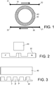
- the invention relates to a device for modulating or switching an optical signal which comprises first and second bus waveguides 10, 20 optically coupled to a first ring waveguide 30.
- the first bus waveguide 10 comprises an input port 11, commonly designated by port “In”, for receiving the optical signal to be modulated or switched and an output port 12, commonly designated by port “Through”.
- the second bus waveguide 20 has an input port 21, commonly known as an "Add” port, and an output port 22, commonly known as a "Drop” port.
- the first ring waveguide 30 has for example a radius of 40 ⁇ m. It is preferably sought to have the largest possible radius to increase the quality factor of the device and its modulation / switching efficiency. On the other hand, this radius is limited by the maximum modulation / switching frequency desired.
- the invention may in this regard advantageously find application for producing switches for which the switching frequency must be less than 1 GHz, or even a few hundred MHz.
- the first ring waveguide 30 is formed from a first material from which is made, typically by doping, at least one p-n or p-i-n junction. By varying the electrical potential at the terminals of this junction, a variation in the concentration of the carriers in the resonant cavity is created, which translates its resonance in the optical spectrum.
- the first material is typically silicon.
- the first material can also be germanium or a III-V material.
- the modulation case is more generic and implies that the signal available on the “Drop” output port 22 is adjusted at different intermediate levels between “ON” and “OFF”, the optical power of the signal to be modulated being therefore partially switched between the "Through” and "Drop” output ports.
- the modulation / switching device comprises a second ring waveguide 40 arranged axially opposite the first guide wave wave 30.
- the first and the second wave wave guide face each other, ie they are arranged opposite one another.
- the first and second waveguides are thus superimposed, with or without a space between them.
- the two ring waveguides 30, 40 are spaced from one another, for example by a distance of 200 nm.
- the distance separating the two ring waveguides 30, 40 must remain small enough to ensure optical coupling between the two ring waveguides. This distance is generally less than 400 nm, and in one possible embodiment, the two ring waveguides can even be placed side by side.
- the second ring waveguide may be above or below the first ring waveguide.
- the dimensions of the second ring waveguide 40 are chosen so as to guarantee single-mode operation at the working wavelength, for example at 1310 nm.
- the second ring waveguide 40 can be a strip guide (guide strip ) having for example a width (transverse to the direction of propagation of the light) of 700 nm and a height of 600 nm.
- the first ring waveguide 30 can be a rib guide ( rib guide) which has for example a central part of 250 nm wide resulting from an etching of 250 nm in depth in a guide of 300 nm of height.
- the first ring waveguide 30 has in its central part a pn junction parallel to the direction of propagation of light in the first ring waveguide.
- This junction is lateral on the figure 2 , but the invention also extends to a vertical junction. In the same way, it can be a pin junction.
- the first ring waveguide may have a plurality of pn or pin junctions arranged orthogonally to the direction of light propagation in the first ring waveguide. In this mode of embodiment, there are thus regions p and n interdigitated along the circumference of the first ring waveguide.
- the second ring waveguide 40 is formed from a second material which has a thermo-optical coefficient lower than the thermo-optical coefficient of the first material of the first ring waveguide 30.
- the second material may be SiN, SinO, AIN or even be a polymer material such as PMMA (polymethyl methacrylate). Materials are preferably chosen such that the thermo-optical coefficient of the second material is at least five times smaller than the thermo-optical coefficient of the first material.
- the thermo-optical coefficient of a silicon nitride can be 2.10 -5 K -1 where the thermo-optical coefficient of silicon is 2.10 -4 K -1 , or up to ten times less depending on filing conditions.
- the invention thus proposes to introduce into a stack of a photonic platform an additional layer of a second material less sensitive to temperature than the material of the first ring waveguide.
- This second material makes it possible to reduce the thermal sensitivity of the modulation / switching device so that it can operate without an active feedback system, at least for slight variations in temperature.
- the bus waveguides 10, 20 can be made of the second material, and thus be arranged in the layer of the stack where the second ring waveguide is found. Alternatively, they can be made of the first material, and thus be arranged in the layer of the stack where the first ring wave guide is found. In an alternative embodiment, the bus waveguides can be arranged in a third layer.
- the invention therefore proposes to use two layers of different materials to form the two ring waveguides facing each other, one (the first) ensuring the active modulation / switching function. and the other (the second) improving the passive properties of the ring.
- the optical signal must have an optical mode distributed over the two ring waveguides 30, 40.
- the second material generally has a much lower index than the first material, so that it is difficult to obtain a coupled mode whose optical power would be distributed over the two ring waveguides.
- the Si index is 3.5 where the SiN index is 1.9.
- the invention proposes that the first ring waveguide 30 forms a subwavelength network.
- its effective index approaches that of the second ring waveguide 40.
- sub-wavelength it is meant that the pitch of the grating is less than ⁇ / 2 n to avoid any diffraction effect, with n the effective index of the coupled mode.
- the period of the subwavelength network can be 350nm.
- the first ring wave guide therefore has along its circumference a set of radial slots F arranged periodically, two successive slots being separated by a pad P of the first material.
- the residual thickness of the first ring waveguide at the slots F is preferably between 50nm (below, the electrical access resistance may be too high) and 100nm (above, a mode propagation of a plate guide is likely to occur).
- the width of the pads P (in the direction of propagation of the light) is chosen in view of the limits on the pitch of the grating and on the manufacturing possibilities for adjusting the effective index of the first ring waveguide, which will controlling the distribution of the optical mode between the first ring waveguide 30 and the second ring waveguide 40.
- the distribution of light between the two ring waveguides is therefore essentially adjusted by adjusting the width of the first ring waveguide (transverse to the direction of light propagation) and the width of the studs (according to the direction of light propagation).
- the first ring waveguide 30 is a resonant device having good quality factors and therefore for which the modulation / switching is particularly effective.
- the modulation / switching efficiency can also be improved by increasing the amplitude of the electric modulation / switching control signal. It is therefore possible to favor an optical mode mainly in the second ring waveguide (to promote thermal insensitivity) without affecting the modulation / switching efficiency.
- the distribution of light between the ring waveguides is such that 5% to 10% of the optical signal is confined in the first ring waveguide.
- the intensity of the coupled mode propagating in the two ring waveguides is to a large extent confined in the second ring waveguide.
- the second material having a low index, the roughness of the walls is less important and the quality factor of the assembly is thereby increased.
- the losses induced by doping the first material are also reduced.
- the sub-lambda nature of the structuring of the first ring wave guide does not degrade the quality factor.
- the quality factor being important, the resonance is finer. It is therefore possible to switch the modulator / switch with a relatively low mode overlap rate by the first material.
- the first ring waveguide is here an Si ring
- the second ring waveguide is an SiN ring
- these ring waveguides are encapsulated in a SiO 2 cladding and their dimensions are those exemplified previously.
- the effective index of the coupled mode is 1.64.
- 80% of the light remains confined there.
Landscapes
- Physics & Mathematics (AREA)
- Nonlinear Science (AREA)
- General Physics & Mathematics (AREA)
- Optics & Photonics (AREA)
- Electromagnetism (AREA)
- Engineering & Computer Science (AREA)
- Computer Networks & Wireless Communication (AREA)
- Signal Processing (AREA)
- Optical Modulation, Optical Deflection, Nonlinear Optics, Optical Demodulation, Optical Logic Elements (AREA)
- Optical Integrated Circuits (AREA)
Applications Claiming Priority (1)
| Application Number | Priority Date | Filing Date | Title |
|---|---|---|---|
| FR1856931A FR3084481B1 (fr) | 2018-07-25 | 2018-07-25 | Modulateur-commutateur athermique a deux anneaux superposes |
Publications (2)
| Publication Number | Publication Date |
|---|---|
| EP3599501A1 true EP3599501A1 (de) | 2020-01-29 |
| EP3599501B1 EP3599501B1 (de) | 2021-10-20 |
Family
ID=65685440
Family Applications (1)
| Application Number | Title | Priority Date | Filing Date |
|---|---|---|---|
| EP19186973.4A Active EP3599501B1 (de) | 2018-07-25 | 2019-07-18 | Athermischer modulator-umschalter mit zwei übereinander angeordneten ringen |
Country Status (3)
| Country | Link |
|---|---|
| US (1) | US10768454B2 (de) |
| EP (1) | EP3599501B1 (de) |
| FR (1) | FR3084481B1 (de) |
Families Citing this family (1)
| Publication number | Priority date | Publication date | Assignee | Title |
|---|---|---|---|---|
| FR3107351B1 (fr) | 2020-02-19 | 2022-02-04 | Commissariat Energie Atomique | Capteur à fibre optique structurée intégrant un dispositif d’émission laser à effet Vernier accordable |
Citations (2)
| Publication number | Priority date | Publication date | Assignee | Title |
|---|---|---|---|---|
| US20090274187A1 (en) * | 2006-01-11 | 2009-11-05 | Koji Kudo | Semiconductor Laser, Module and Optical Transmitter |
| US20140321848A1 (en) * | 2012-01-31 | 2014-10-30 | Fujitsu Limited | Optical transmitter and method for controlling operation state of optical transmitter |
Family Cites Families (16)
| Publication number | Priority date | Publication date | Assignee | Title |
|---|---|---|---|---|
| WO2009055440A2 (en) * | 2007-10-22 | 2009-04-30 | Massachusetts Institute Of Technology | Low-loss bloch wave guiding in open structures and highly compact efficient waveguide-crossing arrays |
| WO2009059182A1 (en) * | 2007-10-31 | 2009-05-07 | Massachusetts Institute Of Technology | Controlling optical resonances via optically induced potentials |
| US8385698B2 (en) * | 2007-12-12 | 2013-02-26 | Hewlett-Packard Development Company, L.P. | Controllable optical ring resonator having periodically spaced control electrodes |
| JP2009258527A (ja) * | 2008-04-21 | 2009-11-05 | Hitachi Ltd | 光学素子 |
| EP2972531A4 (de) * | 2013-03-13 | 2016-12-07 | Hewlett Packard Entpr Dev Lp | Gekoppeltes ringresonatorsystem |
| KR102116977B1 (ko) * | 2013-04-11 | 2020-05-29 | 삼성전자 주식회사 | 비열 광 변조기 및 그 제조 방법 |
| US9690122B2 (en) * | 2014-02-26 | 2017-06-27 | National Institute Of Advanced Industrial Science And Technology | Optical semiconductor device |
| FR3028050B1 (fr) | 2014-10-29 | 2016-12-30 | Commissariat Energie Atomique | Substrat pre-structure pour la realisation de composants photoniques, circuit photonique et procede de fabrication associes |
| WO2016118079A1 (en) * | 2015-01-22 | 2016-07-28 | Agency for Science,Technology and Research | Optical device and method of controlling the same |
| FR3055977B1 (fr) | 2016-09-15 | 2018-09-28 | Commissariat A L'energie Atomique Et Aux Energies Alternatives | Dispositif de couplage optique |
| FR3056306B1 (fr) | 2016-09-20 | 2019-11-22 | Commissariat A L'energie Atomique Et Aux Energies Alternatives | Guide optique presentant un virage a pseudo-gradient d'indice |
| FR3064078B1 (fr) * | 2017-03-17 | 2020-07-24 | Commissariat Energie Atomique | Dispositif optoelectronique de generation d’un peigne de frequences |
| FR3066616B1 (fr) | 2017-05-18 | 2019-06-14 | Commissariat A L'energie Atomique Et Aux Energies Alternatives | Source de lumiere guidee, son procede de fabrication et son utilisation pour l'emission de photons uniques |
| FR3069070A1 (fr) | 2017-07-17 | 2019-01-18 | Commissariat A L'energie Atomique Et Aux Energies Alternatives | Dispositif de focalisation optique a pseudo-gradient d'indice |
| FR3070507B1 (fr) | 2017-08-31 | 2019-09-13 | Commissariat A L'energie Atomique Et Aux Energies Alternatives | Matrice de phases optiques a adressage simplifie |
| FR3071626B1 (fr) | 2017-09-26 | 2019-11-01 | Commissariat A L'energie Atomique Et Aux Energies Alternatives | Dispositif de couplage optique pour un circuit photonique. |
-
2018
- 2018-07-25 FR FR1856931A patent/FR3084481B1/fr active Active
-
2019
- 2019-07-18 EP EP19186973.4A patent/EP3599501B1/de active Active
- 2019-07-22 US US16/518,141 patent/US10768454B2/en active Active
Patent Citations (2)
| Publication number | Priority date | Publication date | Assignee | Title |
|---|---|---|---|---|
| US20090274187A1 (en) * | 2006-01-11 | 2009-11-05 | Koji Kudo | Semiconductor Laser, Module and Optical Transmitter |
| US20140321848A1 (en) * | 2012-01-31 | 2014-10-30 | Fujitsu Limited | Optical transmitter and method for controlling operation state of optical transmitter |
Non-Patent Citations (5)
| Title |
|---|
| BISWAJEET GUHA ET AL: "Athermal silicon microring resonators with titanium oxide cladding", OPTICS EXPRESS, vol. 21, no. 22, 28 October 2013 (2013-10-28), pages 26557, XP055207093, DOI: 10.1364/OE.21.026557 * |
| DE PADMARAJU ET AL.: "Integrated thermal stabilization of a microring modulator", OPT. EXP, 2013 |
| GUHA ET AL.: "Athermal silicon microring resonators with titanium oxide cladding", OPT. EXP., 2013 |
| MOHAMMAD SOLTANI ET AL: "Enabling arbitrary wavelength frequency combs on chip : Enabling arbitrary wavelength frequency combs on chip", LASER & PHOTONICS REVIEWS, vol. 10, no. 1, 1 January 2016 (2016-01-01), DE, pages 158 - 162, XP055440273, ISSN: 1863-8880, DOI: 10.1002/lpor.201500226 * |
| PADMARAJU K ET AL: "Integrated thermal stabilization of a microring modulator", OPTICAL FIBER COMMUNICATION CONFERENCE AND EXPOSITION AND THE NATIONAL FIBER OPTIC ENGINEERS CONFERENCE (OFC/NFOEC), 2013, IEEE, 17 March 2013 (2013-03-17), pages 1 - 3, XP032678941, ISBN: 978-1-4799-0457-0, [retrieved on 20130614] * |
Also Published As
| Publication number | Publication date |
|---|---|
| US20200033645A1 (en) | 2020-01-30 |
| FR3084481B1 (fr) | 2021-07-23 |
| EP3599501B1 (de) | 2021-10-20 |
| FR3084481A1 (fr) | 2020-01-31 |
| US10768454B2 (en) | 2020-09-08 |
Similar Documents
| Publication | Publication Date | Title |
|---|---|---|
| Komljenovic et al. | Heterogeneous silicon photonic integrated circuits | |
| EP2411863B1 (de) | Aus Silizium auf einem Isolator bestehender optischer Breitbandmodulator | |
| Bowers et al. | Recent advances in silicon photonic integrated circuits | |
| CN110058352B (zh) | 检测器再调制器 | |
| CN106104947B (zh) | 可调谐soi激光器 | |
| US8559470B2 (en) | Method and system for hybrid integration of a tunable laser and a phase modulator | |
| EP3015888B1 (de) | Vorstrukturiertes substrat für die herstellung von photonischen komponenten, entsprechender photonenschaltkreis und entsprechendes herstellungsverfahren | |
| US20170082876A1 (en) | Detector remodulator | |
| JP2010027664A (ja) | 光半導体装置 | |
| EP3869160B1 (de) | Strukturierter faseroptischer sensor mit integrierter laser-emissionsvorrichtung mit abstimmbarem noniuseffekt | |
| EP3994509B1 (de) | Anordnung einer aktiven halbleiterbauelements und eines passiven optischen bauteils auf silikonbasis | |
| EP3190672A1 (de) | Laserquelle mit halbleiter | |
| EP3869641B1 (de) | Abstimmbarer vernier-effekt-laser | |
| EP3599501B1 (de) | Athermischer modulator-umschalter mit zwei übereinander angeordneten ringen | |
| Pommarede et al. | Transmission OVER 50km at 10Gbs/s with a hybrid III-V on silicon integrated tunable laser and electro-absorption modulator | |
| Ferrotti | Design, fabrication and characterization of a hybrid III-V on silicon transmitter for high-speed communications. | |
| Mandorlo et al. | Controlled multi-wavelength emission in full cmos compatible micro-lasers for on chip interconnections | |
| JP5164897B2 (ja) | 光フィルタ | |
| Maram et al. | Silicon microring modulator with a pin-diode-loaded multimode interferometer coupler | |
| EP2846424B1 (de) | Integrierte optoelektronische Vorrichtung, die einen Laseremissionsteil und einen Verarbeitungsteil des emittierten optischen Signals umfasst | |
| WO2025027739A1 (en) | Spot size converter and optical integrated device | |
| Liu et al. | Low-power electro-optical switch based on a iii-v microdisk cavity on a silicon-on-insulator circuit | |
| Rong et al. | Recent development on silicon-based Raman lasers and amplifiers | |
| Liu et al. | Silicon high-speed modulators | |
| FR2843494A1 (fr) | Laser largement accordable sur cristal photonique |
Legal Events
| Date | Code | Title | Description |
|---|---|---|---|
| PUAI | Public reference made under article 153(3) epc to a published international application that has entered the european phase |
Free format text: ORIGINAL CODE: 0009012 |
|
| STAA | Information on the status of an ep patent application or granted ep patent |
Free format text: STATUS: REQUEST FOR EXAMINATION WAS MADE |
|
| 17P | Request for examination filed |
Effective date: 20190718 |
|
| AK | Designated contracting states |
Kind code of ref document: A1 Designated state(s): AL AT BE BG CH CY CZ DE DK EE ES FI FR GB GR HR HU IE IS IT LI LT LU LV MC MK MT NL NO PL PT RO RS SE SI SK SM TR |
|
| AX | Request for extension of the european patent |
Extension state: BA ME |
|
| RIC1 | Information provided on ipc code assigned before grant |
Ipc: H04B 10/50 20130101ALI20210331BHEP Ipc: G02F 1/025 20060101ALI20210331BHEP Ipc: G02F 1/015 20060101AFI20210331BHEP |
|
| GRAP | Despatch of communication of intention to grant a patent |
Free format text: ORIGINAL CODE: EPIDOSNIGR1 |
|
| STAA | Information on the status of an ep patent application or granted ep patent |
Free format text: STATUS: GRANT OF PATENT IS INTENDED |
|
| INTG | Intention to grant announced |
Effective date: 20210528 |
|
| GRAS | Grant fee paid |
Free format text: ORIGINAL CODE: EPIDOSNIGR3 |
|
| GRAA | (expected) grant |
Free format text: ORIGINAL CODE: 0009210 |
|
| STAA | Information on the status of an ep patent application or granted ep patent |
Free format text: STATUS: THE PATENT HAS BEEN GRANTED |
|
| AK | Designated contracting states |
Kind code of ref document: B1 Designated state(s): AL AT BE BG CH CY CZ DE DK EE ES FI FR GB GR HR HU IE IS IT LI LT LU LV MC MK MT NL NO PL PT RO RS SE SI SK SM TR |
|
| REG | Reference to a national code |
Ref country code: GB Ref legal event code: FG4D Free format text: NOT ENGLISH |
|
| REG | Reference to a national code |
Ref country code: CH Ref legal event code: EP |
|
| REG | Reference to a national code |
Ref country code: DE Ref legal event code: R096 Ref document number: 602019008481 Country of ref document: DE |
|
| REG | Reference to a national code |
Ref country code: IE Ref legal event code: FG4D Free format text: LANGUAGE OF EP DOCUMENT: FRENCH |
|
| REG | Reference to a national code |
Ref country code: AT Ref legal event code: REF Ref document number: 1440419 Country of ref document: AT Kind code of ref document: T Effective date: 20211115 |
|
| REG | Reference to a national code |
Ref country code: LT Ref legal event code: MG9D |
|
| REG | Reference to a national code |
Ref country code: NL Ref legal event code: MP Effective date: 20211020 |
|
| REG | Reference to a national code |
Ref country code: AT Ref legal event code: MK05 Ref document number: 1440419 Country of ref document: AT Kind code of ref document: T Effective date: 20211020 |
|
| PG25 | Lapsed in a contracting state [announced via postgrant information from national office to epo] |
Ref country code: RS Free format text: LAPSE BECAUSE OF FAILURE TO SUBMIT A TRANSLATION OF THE DESCRIPTION OR TO PAY THE FEE WITHIN THE PRESCRIBED TIME-LIMIT Effective date: 20211020 Ref country code: LT Free format text: LAPSE BECAUSE OF FAILURE TO SUBMIT A TRANSLATION OF THE DESCRIPTION OR TO PAY THE FEE WITHIN THE PRESCRIBED TIME-LIMIT Effective date: 20211020 Ref country code: FI Free format text: LAPSE BECAUSE OF FAILURE TO SUBMIT A TRANSLATION OF THE DESCRIPTION OR TO PAY THE FEE WITHIN THE PRESCRIBED TIME-LIMIT Effective date: 20211020 Ref country code: BG Free format text: LAPSE BECAUSE OF FAILURE TO SUBMIT A TRANSLATION OF THE DESCRIPTION OR TO PAY THE FEE WITHIN THE PRESCRIBED TIME-LIMIT Effective date: 20220120 Ref country code: AT Free format text: LAPSE BECAUSE OF FAILURE TO SUBMIT A TRANSLATION OF THE DESCRIPTION OR TO PAY THE FEE WITHIN THE PRESCRIBED TIME-LIMIT Effective date: 20211020 |
|
| PG25 | Lapsed in a contracting state [announced via postgrant information from national office to epo] |
Ref country code: IS Free format text: LAPSE BECAUSE OF FAILURE TO SUBMIT A TRANSLATION OF THE DESCRIPTION OR TO PAY THE FEE WITHIN THE PRESCRIBED TIME-LIMIT Effective date: 20220220 Ref country code: SE Free format text: LAPSE BECAUSE OF FAILURE TO SUBMIT A TRANSLATION OF THE DESCRIPTION OR TO PAY THE FEE WITHIN THE PRESCRIBED TIME-LIMIT Effective date: 20211020 Ref country code: PT Free format text: LAPSE BECAUSE OF FAILURE TO SUBMIT A TRANSLATION OF THE DESCRIPTION OR TO PAY THE FEE WITHIN THE PRESCRIBED TIME-LIMIT Effective date: 20220221 Ref country code: PL Free format text: LAPSE BECAUSE OF FAILURE TO SUBMIT A TRANSLATION OF THE DESCRIPTION OR TO PAY THE FEE WITHIN THE PRESCRIBED TIME-LIMIT Effective date: 20211020 Ref country code: NO Free format text: LAPSE BECAUSE OF FAILURE TO SUBMIT A TRANSLATION OF THE DESCRIPTION OR TO PAY THE FEE WITHIN THE PRESCRIBED TIME-LIMIT Effective date: 20220120 Ref country code: NL Free format text: LAPSE BECAUSE OF FAILURE TO SUBMIT A TRANSLATION OF THE DESCRIPTION OR TO PAY THE FEE WITHIN THE PRESCRIBED TIME-LIMIT Effective date: 20211020 Ref country code: LV Free format text: LAPSE BECAUSE OF FAILURE TO SUBMIT A TRANSLATION OF THE DESCRIPTION OR TO PAY THE FEE WITHIN THE PRESCRIBED TIME-LIMIT Effective date: 20211020 Ref country code: HR Free format text: LAPSE BECAUSE OF FAILURE TO SUBMIT A TRANSLATION OF THE DESCRIPTION OR TO PAY THE FEE WITHIN THE PRESCRIBED TIME-LIMIT Effective date: 20211020 Ref country code: GR Free format text: LAPSE BECAUSE OF FAILURE TO SUBMIT A TRANSLATION OF THE DESCRIPTION OR TO PAY THE FEE WITHIN THE PRESCRIBED TIME-LIMIT Effective date: 20220121 Ref country code: ES Free format text: LAPSE BECAUSE OF FAILURE TO SUBMIT A TRANSLATION OF THE DESCRIPTION OR TO PAY THE FEE WITHIN THE PRESCRIBED TIME-LIMIT Effective date: 20211020 |
|
| REG | Reference to a national code |
Ref country code: DE Ref legal event code: R097 Ref document number: 602019008481 Country of ref document: DE |
|
| PG25 | Lapsed in a contracting state [announced via postgrant information from national office to epo] |
Ref country code: SM Free format text: LAPSE BECAUSE OF FAILURE TO SUBMIT A TRANSLATION OF THE DESCRIPTION OR TO PAY THE FEE WITHIN THE PRESCRIBED TIME-LIMIT Effective date: 20211020 Ref country code: SK Free format text: LAPSE BECAUSE OF FAILURE TO SUBMIT A TRANSLATION OF THE DESCRIPTION OR TO PAY THE FEE WITHIN THE PRESCRIBED TIME-LIMIT Effective date: 20211020 Ref country code: RO Free format text: LAPSE BECAUSE OF FAILURE TO SUBMIT A TRANSLATION OF THE DESCRIPTION OR TO PAY THE FEE WITHIN THE PRESCRIBED TIME-LIMIT Effective date: 20211020 Ref country code: EE Free format text: LAPSE BECAUSE OF FAILURE TO SUBMIT A TRANSLATION OF THE DESCRIPTION OR TO PAY THE FEE WITHIN THE PRESCRIBED TIME-LIMIT Effective date: 20211020 Ref country code: DK Free format text: LAPSE BECAUSE OF FAILURE TO SUBMIT A TRANSLATION OF THE DESCRIPTION OR TO PAY THE FEE WITHIN THE PRESCRIBED TIME-LIMIT Effective date: 20211020 Ref country code: CZ Free format text: LAPSE BECAUSE OF FAILURE TO SUBMIT A TRANSLATION OF THE DESCRIPTION OR TO PAY THE FEE WITHIN THE PRESCRIBED TIME-LIMIT Effective date: 20211020 |
|
| PLBE | No opposition filed within time limit |
Free format text: ORIGINAL CODE: 0009261 |
|
| STAA | Information on the status of an ep patent application or granted ep patent |
Free format text: STATUS: NO OPPOSITION FILED WITHIN TIME LIMIT |
|
| 26N | No opposition filed |
Effective date: 20220721 |
|
| PG25 | Lapsed in a contracting state [announced via postgrant information from national office to epo] |
Ref country code: AL Free format text: LAPSE BECAUSE OF FAILURE TO SUBMIT A TRANSLATION OF THE DESCRIPTION OR TO PAY THE FEE WITHIN THE PRESCRIBED TIME-LIMIT Effective date: 20211020 |
|
| PG25 | Lapsed in a contracting state [announced via postgrant information from national office to epo] |
Ref country code: SI Free format text: LAPSE BECAUSE OF FAILURE TO SUBMIT A TRANSLATION OF THE DESCRIPTION OR TO PAY THE FEE WITHIN THE PRESCRIBED TIME-LIMIT Effective date: 20211020 |
|
| PG25 | Lapsed in a contracting state [announced via postgrant information from national office to epo] |
Ref country code: MC Free format text: LAPSE BECAUSE OF FAILURE TO SUBMIT A TRANSLATION OF THE DESCRIPTION OR TO PAY THE FEE WITHIN THE PRESCRIBED TIME-LIMIT Effective date: 20211020 |
|
| REG | Reference to a national code |
Ref country code: CH Ref legal event code: PL |
|
| REG | Reference to a national code |
Ref country code: BE Ref legal event code: MM Effective date: 20220731 |
|
| PG25 | Lapsed in a contracting state [announced via postgrant information from national office to epo] |
Ref country code: LU Free format text: LAPSE BECAUSE OF NON-PAYMENT OF DUE FEES Effective date: 20220718 Ref country code: LI Free format text: LAPSE BECAUSE OF NON-PAYMENT OF DUE FEES Effective date: 20220731 Ref country code: CH Free format text: LAPSE BECAUSE OF NON-PAYMENT OF DUE FEES Effective date: 20220731 |
|
| PG25 | Lapsed in a contracting state [announced via postgrant information from national office to epo] |
Ref country code: IT Free format text: LAPSE BECAUSE OF FAILURE TO SUBMIT A TRANSLATION OF THE DESCRIPTION OR TO PAY THE FEE WITHIN THE PRESCRIBED TIME-LIMIT Effective date: 20211020 Ref country code: BE Free format text: LAPSE BECAUSE OF NON-PAYMENT OF DUE FEES Effective date: 20220731 |
|
| PG25 | Lapsed in a contracting state [announced via postgrant information from national office to epo] |
Ref country code: IE Free format text: LAPSE BECAUSE OF NON-PAYMENT OF DUE FEES Effective date: 20220718 |
|
| PG25 | Lapsed in a contracting state [announced via postgrant information from national office to epo] |
Ref country code: HU Free format text: LAPSE BECAUSE OF FAILURE TO SUBMIT A TRANSLATION OF THE DESCRIPTION OR TO PAY THE FEE WITHIN THE PRESCRIBED TIME-LIMIT; INVALID AB INITIO Effective date: 20190718 |
|
| PG25 | Lapsed in a contracting state [announced via postgrant information from national office to epo] |
Ref country code: MK Free format text: LAPSE BECAUSE OF FAILURE TO SUBMIT A TRANSLATION OF THE DESCRIPTION OR TO PAY THE FEE WITHIN THE PRESCRIBED TIME-LIMIT Effective date: 20211020 Ref country code: CY Free format text: LAPSE BECAUSE OF FAILURE TO SUBMIT A TRANSLATION OF THE DESCRIPTION OR TO PAY THE FEE WITHIN THE PRESCRIBED TIME-LIMIT Effective date: 20211020 |
|
| PG25 | Lapsed in a contracting state [announced via postgrant information from national office to epo] |
Ref country code: MT Free format text: LAPSE BECAUSE OF FAILURE TO SUBMIT A TRANSLATION OF THE DESCRIPTION OR TO PAY THE FEE WITHIN THE PRESCRIBED TIME-LIMIT Effective date: 20211020 |
|
| PGFP | Annual fee paid to national office [announced via postgrant information from national office to epo] |
Ref country code: DE Payment date: 20250722 Year of fee payment: 7 |
|
| PGFP | Annual fee paid to national office [announced via postgrant information from national office to epo] |
Ref country code: GB Payment date: 20250724 Year of fee payment: 7 |
|
| PGFP | Annual fee paid to national office [announced via postgrant information from national office to epo] |
Ref country code: FR Payment date: 20250722 Year of fee payment: 7 |
|
| PG25 | Lapsed in a contracting state [announced via postgrant information from national office to epo] |
Ref country code: TR Free format text: LAPSE BECAUSE OF FAILURE TO SUBMIT A TRANSLATION OF THE DESCRIPTION OR TO PAY THE FEE WITHIN THE PRESCRIBED TIME-LIMIT Effective date: 20211020 |