EP0945734A2 - Verfahren fur das nicht-destruktive Messen von Dopierungskonzentrationen - Google Patents
Verfahren fur das nicht-destruktive Messen von Dopierungskonzentrationen Download PDFInfo
- Publication number
- EP0945734A2 EP0945734A2 EP99105745A EP99105745A EP0945734A2 EP 0945734 A2 EP0945734 A2 EP 0945734A2 EP 99105745 A EP99105745 A EP 99105745A EP 99105745 A EP99105745 A EP 99105745A EP 0945734 A2 EP0945734 A2 EP 0945734A2
- Authority
- EP
- European Patent Office
- Prior art keywords
- dut
- voltage
- transistor
- length
- capacitance
- Prior art date
- Legal status (The legal status is an assumption and is not a legal conclusion. Google has not performed a legal analysis and makes no representation as to the accuracy of the status listed.)
- Withdrawn
Links
- 239000002019 doping agent Substances 0.000 title claims abstract description 43
- 238000000034 method Methods 0.000 title claims abstract description 26
- 238000005259 measurement Methods 0.000 title claims description 16
- 239000012535 impurity Substances 0.000 claims abstract description 29
- 239000004065 semiconductor Substances 0.000 claims abstract description 25
- 229910044991 metal oxide Inorganic materials 0.000 claims abstract description 7
- 150000004706 metal oxides Chemical class 0.000 claims abstract description 7
- 239000000758 substrate Substances 0.000 claims description 9
- 238000005516 engineering process Methods 0.000 claims description 7
- 230000015556 catabolic process Effects 0.000 claims description 6
- 238000012360 testing method Methods 0.000 claims description 6
- 239000012212 insulator Substances 0.000 claims description 5
- 230000001066 destructive effect Effects 0.000 claims description 4
- 230000008859 change Effects 0.000 claims description 3
- 230000005684 electric field Effects 0.000 claims description 3
- 238000004519 manufacturing process Methods 0.000 claims description 3
- 238000012938 design process Methods 0.000 claims description 2
- 238000004422 calculation algorithm Methods 0.000 abstract description 6
- 239000003990 capacitor Substances 0.000 description 12
- 230000003287 optical effect Effects 0.000 description 8
- VYPSYNLAJGMNEJ-UHFFFAOYSA-N Silicium dioxide Chemical compound O=[Si]=O VYPSYNLAJGMNEJ-UHFFFAOYSA-N 0.000 description 6
- 229910052814 silicon oxide Inorganic materials 0.000 description 5
- 238000010586 diagram Methods 0.000 description 4
- 125000004429 atom Chemical group 0.000 description 2
- 230000004888 barrier function Effects 0.000 description 2
- 210000000746 body region Anatomy 0.000 description 2
- 238000004364 calculation method Methods 0.000 description 2
- 230000001419 dependent effect Effects 0.000 description 2
- 230000000779 depleting effect Effects 0.000 description 2
- 230000009977 dual effect Effects 0.000 description 2
- 238000010894 electron beam technology Methods 0.000 description 2
- 150000002500 ions Chemical class 0.000 description 2
- 229910052710 silicon Inorganic materials 0.000 description 2
- 239000010703 silicon Substances 0.000 description 2
- 239000000969 carrier Substances 0.000 description 1
- 238000009795 derivation Methods 0.000 description 1
- 238000013461 design Methods 0.000 description 1
- 238000009792 diffusion process Methods 0.000 description 1
- 238000012544 monitoring process Methods 0.000 description 1
- 230000007935 neutral effect Effects 0.000 description 1
- 125000004437 phosphorous atom Chemical group 0.000 description 1
- 230000005855 radiation Effects 0.000 description 1
- 230000004044 response Effects 0.000 description 1
- 230000001360 synchronised effect Effects 0.000 description 1
Images


Classifications
-
- H—ELECTRICITY
- H01—ELECTRIC ELEMENTS
- H01L—SEMICONDUCTOR DEVICES NOT COVERED BY CLASS H10
- H01L22/00—Testing or measuring during manufacture or treatment; Reliability measurements, i.e. testing of parts without further processing to modify the parts as such; Structural arrangements therefor
-
- H—ELECTRICITY
- H01—ELECTRIC ELEMENTS
- H01L—SEMICONDUCTOR DEVICES NOT COVERED BY CLASS H10
- H01L22/00—Testing or measuring during manufacture or treatment; Reliability measurements, i.e. testing of parts without further processing to modify the parts as such; Structural arrangements therefor
- H01L22/10—Measuring as part of the manufacturing process
- H01L22/14—Measuring as part of the manufacturing process for electrical parameters, e.g. resistance, deep-levels, CV, diffusions by electrical means
-
- H—ELECTRICITY
- H01—ELECTRIC ELEMENTS
- H01L—SEMICONDUCTOR DEVICES NOT COVERED BY CLASS H10
- H01L2924/00—Indexing scheme for arrangements or methods for connecting or disconnecting semiconductor or solid-state bodies as covered by H01L24/00
- H01L2924/0001—Technical content checked by a classifier
- H01L2924/0002—Not covered by any one of groups H01L24/00, H01L24/00 and H01L2224/00
Definitions
- This invention relates to a method for non-destructive measurement by means of a beam of radiant energy, and a corresponding induced signal current dopant impurity concentrations which may vary along the length of certain semiconductor devices, such as lateral double diffused metal oxide semiconductor (LDMOS) transistors which are designed for high voltage (HV) applications.
- LDMOS lateral double diffused metal oxide semiconductor
- an induced current can be generated in a semiconductor having a p-n junction or Schottky Barrier (metal-semicondcutor rectifying contact) by shining a focused beam of radiation of above bandgap energy on the body of the semiconductor.
- Apparatus for generating such beams and for scanning them across a device under test (DUT) are commercially available.
- a large area device such as a high-voltage HV LDMOS transistor (which typically is ten or more microns in length) it is convenient to use a laser beam focused through an optical microscope to illuminate and scan the device.
- EBIC electron beam
- High voltage HV LDMOS devices particularly those fabricated utilizing the reduced surface electric field (RESURF) principle, generally require very specific (e.g., linearly increasing) doping profiles in the drift region of the device.
- a voltage-capacitance relationship internally of a LDMOS transistor determines a space charge region depletion width "W" in the transistor as a function of an applied reverse bias voltage as the transistor is scanned by a laser (or other radiant energy) beam.
- This reverse bias voltage determines how many trapped positive (donor) ions can be uncovered in the graded-dopant n-type drift region of the transistor and results in a fixed depletion width W for each applied voltage.
- a beam-induced photocurrent signal from the LDMOS device under reverse bias allows the measurement of the depletion width W as a function of applied reverse bias voltage.
- a device under test such as a high voltage HV LDMOS transistor
- a laser beam of suitable wavelength and intensity focused onto the DUT through a microscope.
- An optical beam induced current (OBIC) signal is obtained and by the amplitude of the OBIC signal and the beam position along the length of the DUT a respective depletion width (W) is determined for each of a number of values of reverse bias voltage. From these measurements the corresponding dopant impurity concentration (e.g., of phosphorous atoms) for each measured depletion width W is obtained using a mathematical algorithm. This allows determination of a profile of the dopant impurity concentrations as a function of drift region distance or depletion width W in the LDMOS device.
- OBIC optical beam induced current
- An OBIC laser-microscope system does not directly measure internal capacitance of the p-n junction between p+ body and n-type drift region of an LDMOS transistor by conventional electrical measurements, but measures instead the depletion layer capacitance via the space charge region depletion width W. This is another way of measuring the junction depletion layer capacitance resulting from the fixed charge of the uncovered ionized impurity atoms in the space charge region.
- a mathematical equation (described in detail hereinafter) is formulated in a way applicable to the case of OBIC measurements of the DUT to describe the incremental junction capacitance as a function of reverse bias voltage in terms of the space charge region depletion width W and its derivatives.
- the space charge region is further extended in order to achieve higher breakdown voltages by simultaneously depleting vertically from the p-n junction in the device and also horizontally from a substrate oxide layer via an MOS capacitance for the given example of an HV LDMOS device fabricated in SOI (silicon-on insulator) technology.
- MOS capacitance for the given example of an HV LDMOS device fabricated in SOI (silicon-on insulator) technology.
- the added MOS capacitance from the substrate lies in parallel with the depletion layer capacitance of the p-n junction between the p+type body and n-type drift region as will be described hereinafter.
- the depletion layer capacitance of the p-n junction gives only a negligible contribution in this case, since the area of the p-n junction capacitor is negligibly small in comparison with the oxide layer capacitance.
- the MOS capacitance formed by the device substrate and the insulating oxide layer completely dominates the depletion width W in the drift region of the device. Accordingly, as will be explained hereinafter, a further extended mathematical algorithm is derived by means of which are determined in accordance with the invention dopant impurity concentrations in HV LDMOS transistors in SOI technology utilizing the RESURF principle.
- a method for non-destructive measurement of dopant concentrations in the drift region of semiconductor devices comprising a first step of reverse basing a device under test (DUT) with a first voltage, a second step of scanning the device with a beam of radiant energy to induce in the DUT a signal current which varies as the beam scans along the DUT and is used to measure a first depletion width (W) in the DUT, additional steps of repeating the first and second steps using a plurality of separate bias voltages and measuring respective depletion widths W in the DUT, and a final step of determining from the voltages and the widths W a profile of dopant impurity concentrations in the DUT.
- DUT device under test
- W depletion width
- N D dopant impurity concentrations
- the method comprises the steps of: reverse basing the device with a voltage V which can be varied over a wide range until the onset of avalanche breakdown of the device; scanning along a length of the device with a beam of radiant energy to produce in the device a beam induced current signal; using the induced signal to measure a depletion width W in the device for a respective voltage V, the induced OBIC photocurrent signal having a high generally constant value within a region of the depletion width W and decaying generally to zero outside the region, the depletion width W increasing as bias voltage V in increased; repeating the above steps with different bias voltages to establish a series of such voltages V and respective widths W; and determining from interrelationships of voltage V, width W, capacitance (C) and dopant concentration N D , the respective dopant concentrations N D at points along the length of the device.
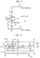
- FIG. 1 there is shown an optical beam scanning apparatus 10 utilized in accordance with a method of the present invention to measure dopant concentrations along the length of a semiconductor device under test (DUT) 12, such as a HV LDMOS transistor.
- the apparatus 10 comprises a laser 14 which emits a beam 16, a polarizer 18, a deflection mirror system 20, a microscope 22 which focuses the beam 16 in a fine spot on the DUT 12, a power source 24, a signal amplifier 26, a signal mixer 28, a raster generator 30, a cathode ray tube (CRT) display 32, and a personal computer (PC) 34.
- the laser 14 emits a beam 16 of light with a wavelength, for example, of 633 nanometers (nm) and of suitable intensity (e.g., several watts).
- the beam 16 passes through a polarizer 18 and into the deflection mirror system 20.
- the mirror system 20 includes a plurality of moveable mirrors 40 and 42 which are driven back and forth by electrical signals received via a lead 44 from the raster generator 30. Mechanical movement of the mirrors 40 and 42 deflects the beam 16 back-and-forth and side-to-side in synchronism with electrical signals from the generator 30 as is well known.
- the beam 16 passes from the deflection mirror system 20 and into the microscope 22 which focuses the beam 16 into a fine spot (e.g., about a micron in diameter) onto a surface of the DUT 12. This results in optical beam induced current (OBIC) in the DUT 12.
- OBIC optical beam induced current
- the beam 16 as it is being deflected by the deflection system 20 thus scans line by line along a length of the DUT 12 and is synchronized with the CRT signal display.
- the DUT 12 is reverse biased by a positive voltage (+V) from the power source 24, a negative side of which is grounded, and a load resistor (R L ) 46.
- a photo-response current passes from the DUT 12 through a sensing resistor (R s ) 48 to ground.
- a signal, termed “Isignal” is applied from the sensing resistor 48 via a lead 50 to an input of the amplifier 26, an output of which is applied via a lead 52 to one input (S) of the signal mixer 28.
- a raster signal is applied to another input (R) of the signal mixer 28 via a lead 54 from the raster generator 30.
- Dual signals (R+S) from the signal mixer 28 are applied via a common connection 56 to an input of the CRT display 32 where the signals are displayed on a screen 58 as a waveform (to be discussed hereinafter) having the usual x and y coordinates.
- the dual R+S signals on the common connection 56 are also applied to the personal computer 32 where they are processed and the dopant impurity concentrations along the length of the DUT 12 are obtained, as will be explained hereinafter.
- the DUT 12 is, by way of example, a HV LDMOS P channel transistor 62 having a drain 64, a gate 65, and a source 66. It is to be understood, however, that the DUT 12 may be a semiconductor other than the transistor 62 shown here (see, for example, Fig. 5).
- the transistor 62 while being scanned by the beam 16 is reverse-biased with its drain 64 connected via the load resistor (R L ) 46 (see FIG. 1) to a positive terminal 68(+V) of the power supply 24 (not shown here but shown in FIG.
- the negative side of the supply being connected to a terminal 69 and to ground.
- the gate 65 of the transistor 62 is connected directly to ground and the terminal 69 (-V) which is shown connected to ground while the source 66 is connected via the sensing resistor (R S ) 48 to ground.
- a voltage across the sensing resistor 48 is proportional to OBIC current as the DUT 12 is scanned by the beam 16, as was previously explained. This voltage is applied to the lead 50 (see Fig. 1) and is termed "Isignal"
- the supply voltage +V can be varied over a wide range until the onset of avalanche breakdown of the particular device.
- the resistor (R L ) 46 may have a value of 100 K ohms
- the resistor (R S ) 48 a value of 10 K ohms
- the resistance in reverse bias across the drain 64 and the source 66 of the transistor 62 may be approximately 100M ohms.
- the relative sizes of these resistances result in the voltage at the drain 64 of the transistor 62 being substantially at the supply voltage +V, and the source 66 being substantially at ground (-V).
- the DUT 12 comprising the transistor 62 shown in this simplified example as a lateral high voltage diode.
- Distance along the length of the DUT 12 is indicated at "x”
- a first shaded area of the DUT 12 represents a p+type body region 72
- an unshaded area on both sides of the P-N junction 70 represents an unsymmetrical space charge region 74
- a second shaded area represents the remainder of an n-type drift region 76.
- the unshaded area represents the depletion region adjacent to the p-n junction 70 of the DUT 12 where all of the laser induced photo-generated electron-hole pairs are separated and collected by the high local field applied by the reverse bias voltage, giving rise to the OBIC photocurrent.
- the second shaded area indicates a neutral n-type drift region 76 outside of the depletion region (space charge region 74) where the photo-generated carriers are not collected any more and no OBIC photocurrent is measured.
- Electrical connections to the DUT 12 are not shown here but are as shown in FIG. 2.
- the drain 64 and the source 66 of the DUT 12 are as schematically indicated in FIG. 3 at opposite ends of the DUT 12.
- the DUT 12 has an internal capacitance across its p-n junction 70. This is schematically illustrated in dashed outline in Fig. 3 by a capacitor (C) 79 which is coupled between the drain 64 and the source 66 of the DUT 12.
- the voltage at the drain 64 is indicated here as "+V D ".
- this voltage capacitance relationship determines the space charge region depletion width W as a function of the applied reverse bias voltage of a LDMOS transistor.
- the reverse bias voltage determines how many trapped positive ions can be uncovered in the graded n-type drift region and results in a fixed depletion width W for each applied voltage.
- the OBIC photocurrent signal on the LDMOS device under reverse bias allows the measurement of the depletion width W as a function of applied reverse bias voltage. From these measurements the corresponding dopant impurity concentration for each measured depletion width W can be obtained by means of a mathematical algorithm. This in turn allows a profiling of the dopant impurity concentration as a function of drift region distance or depletion width W in the LDMOS device (e.g., the transistor 62).
- FIG. 4 there is shown a graph 80 of a somewhat idealized waveform 82 of Isignal.
- the horizontal axis of the graph 80 represents distance in the x direction along the DUT 12 (FIG. 3).
- the vertical axis of the graph 80 represents the magnitude of Isignal with a normalized level of 1.0 representing the maximum measured value.
- the horizontal portion 90 of the waveform 82 is a measure of the depletion width W, and the length of the portion 90 in the x direction is a function of the bias voltage applied by the power source 24 (FIGS.
- a first darkly shaded area of the transistor 102 represents a p+type body region 104, a lightly shaded (crosshatched) area over the p-n junction 102 represents an unsymmetrical space charge region 106, a second darkly shaded area represents an n-type drift region 108, and a third darkly shaded area represents an n+type substrate 110, which is grounded.
- An unshaded area represents a horizontal layer 112 of silicon oxide (SiO 2 ) separating and insulating the substrate 110 from the upper portions 104, 106 and 108 of the transistor 100. Electrical connections to the transistor 100 are not shown here but are like those shown in FIG. 2 for the transistor 62.
- the drain 116 and the source 118 of the transistor 100 are as schematically indicated in FIG. 5 at opposite ends of the transistor 100. Its gate (not shown) is grounded.
- the transistor 100 has an internal capacitance across its p-n junction 102 as schematically illustrated in dashed outline in FIG. 5 by a capacitor (C 1 ) 130 which is shown coupled between a voltage "+V D " at the drain 116 of the transistor 100 and ground. Also shown in dashed outline coupled in series between "+V D " and ground are a depletion layer capacitance, illustrated by a capacitor (C 2 ) 132 and an insulating layer (SiO 2 ) capacitance illustrated by a capacitor (C 3 ) 134.
- the area of the p-n junction 102 which determines the size of the capacitor 130, is negligibly small in comparison with the depletion layer area (and capacitor 132) and the oxide layer area (and capacitor 134). Thus capacitor 130 can be neglected, and only capacitors 132 and 134 in series need be considered.
- An OBIC, and signal (like the waveform 82 of FIG. 4) are generated in the transistor 100 (in its role as the DUT 12) as it is scanned by the laser beam 16.
- the space charge region is further extended in order to achieve higher breakdown voltages by simultaneously depleting vertically from the p-n junction in the device and also horizontally from a bottom oxide layer via an added capacitance.
- the depletion layer capacitance (C 1 ) of the p-n junction gives only a negligible contribution in this case, since the area of the p-n junction is negligible.
- Equation 2 the series capacitance (C 2 and C 3 ) formed by the device substrate and the insulating oxide layer completely dominates the depletion width W in the drift region of the transistor 100. Equation 2 above does not apply in this case. However, a further extended mathematical derivation of Equation 1, as is easily understood by those skilled in the art, permits profiling of dopant impurity concentration in the transistor 100.
- N D k 2 ox_o [V-(kT/q)In(N D /n i )] 2 2 d 2 ox k s q(kT/q)In(N D /n i ) where:
- Equation 3 the quantity N D is expressed as a function of itself. Accordingly Equation 3 is best solved for N D by successive approximations of N D starting with an assumed (guessed) value of N D . The correct value of N D for a measured set of conditions will be obtained after a few iterations using successive values of N D closer and closer to the actual value, as is well known. This will be illustrated below for a specific set of iterations of N D in a particular example of dopant concentration in a transistor 100.
- the values of N D in Column 3 are determined by use of Equation 3.
- the value of N D of 3.204 x 10 16 in Row 1 corresponding to a reverse bias of 30V and a depletion width W of 7.72 microns, is calculated as follows.
- the N D equals 5 x 10 16 and this value is entered for N D on the right hand side of Equation 3 for a first iteration.
- the resulting calculation gives 3.1073 x 10 16 for N D .
- This latter value in a second iteration of Equation 3 results in a calculated value of 3.2114 x 10 16 .
- a third iteration of Equation 3 gives a value of 3.2039 x 10 16 for N D .
- N D calculations of N D outlined above are performed in the personal computer (PC) 34 (Fig. 1) using a suitable mathematical algorithm, as is well understood by those skilled in the art.
- the additional values of N D in Rows 2-16 of the Table, corresponding to respective values of V and W, are arrived at in the same way.
- Column 3 of the Table is thus a profile of dopant impurity concentrations along the length of the DUT 12 (e.g., transistor 100). It should be noted that here the dopant profile increases approximately linearly with increasing length.
- the above description is intended in illustration and not in limitation of the invention.
- Various changes in the apparatus described and in the method of the invention as set forth may occur to those skilled in the art, and these changes may be made without departing from the spirit or scope of the invention as set forth in the accompanying claims.
- the invention is not limited solely to application with the transistors illustrated in Figs. 3 and 5, but is applicable to other semiconductor devices such as semiconductor lateral high voltage diodes as well as any other class of electronic devices amenable to p-n junction probing. Schottky barrier probing, or MOS capacitor probing by OBIC or EBIC.
- the invention is not limited to measurement of dopant impurity concentrations which vary linearly with length along a semiconductor device.
Applications Claiming Priority (2)
| Application Number | Priority Date | Filing Date | Title |
|---|---|---|---|
| US7972098P | 1998-03-27 | 1998-03-27 | |
| US79720P | 1998-03-27 |
Publications (2)
| Publication Number | Publication Date |
|---|---|
| EP0945734A2 true EP0945734A2 (de) | 1999-09-29 |
| EP0945734A3 EP0945734A3 (de) | 1999-12-01 |
Family
ID=22152368
Family Applications (1)
| Application Number | Title | Priority Date | Filing Date |
|---|---|---|---|
| EP99105745A Withdrawn EP0945734A3 (de) | 1998-03-27 | 1999-03-22 | Verfahren fur das nicht-destruktive Messen von Dopierungskonzentrationen |
Country Status (6)
| Country | Link |
|---|---|
| US (1) | US6294919B1 (de) |
| EP (1) | EP0945734A3 (de) |
| JP (1) | JPH11340293A (de) |
| KR (1) | KR19990078175A (de) |
| CN (1) | CN1243948A (de) |
| TW (1) | TW429321B (de) |
Families Citing this family (14)
| Publication number | Priority date | Publication date | Assignee | Title |
|---|---|---|---|---|
| US6897440B1 (en) * | 1998-11-30 | 2005-05-24 | Fab Solutions, Inc. | Contact hole standard test device |
| JP3749107B2 (ja) * | 1999-11-05 | 2006-02-22 | ファブソリューション株式会社 | 半導体デバイス検査装置 |
| JP3874996B2 (ja) * | 2000-05-30 | 2007-01-31 | ファブソリューション株式会社 | デバイス検査方法および装置 |
| JP3847568B2 (ja) * | 2001-03-01 | 2006-11-22 | ファブソリューション株式会社 | 半導体装置製造方法 |
| JP4738610B2 (ja) * | 2001-03-02 | 2011-08-03 | 株式会社トプコン | 基板表面の汚染評価方法及び汚染評価装置と半導体装置の製造方法 |
| JP3913555B2 (ja) | 2002-01-17 | 2007-05-09 | ファブソリューション株式会社 | 膜厚測定方法および膜厚測定装置 |
| US6815950B2 (en) * | 2002-07-24 | 2004-11-09 | Schlumberger Technology Corporation | J-spectroscopy in the wellbore |
| US6963393B2 (en) * | 2002-09-23 | 2005-11-08 | Applied Materials, Inc. | Measurement of lateral diffusion of diffused layers |
| JP2006093257A (ja) * | 2004-09-22 | 2006-04-06 | Fuji Electric Holdings Co Ltd | 半導体素子の微小領域の電気物性測定方法 |
| CN101034671B (zh) * | 2006-03-02 | 2010-12-08 | 沃特拉半导体公司 | 横向双扩散金属氧化物半导体场效应晶体管及其制造方法 |
| JP5892597B2 (ja) * | 2012-02-24 | 2016-03-23 | 株式会社Screenホールディングス | 検査装置および検査方法 |
| US9733297B2 (en) | 2013-02-19 | 2017-08-15 | Hamamatsu Photonics K.K. | Electric field concentration location observation device and electric field concentration location observation method |
| US9103659B1 (en) * | 2014-02-27 | 2015-08-11 | Tsmc Solar Ltd. | Method and system for junction depth identification for ultra shallow junctions |
| CN103943531A (zh) * | 2014-04-22 | 2014-07-23 | 上海华力微电子有限公司 | 在线监控锗硅工艺中自掺杂硼浓度的方法 |
Citations (1)
| Publication number | Priority date | Publication date | Assignee | Title |
|---|---|---|---|---|
| EP0555133A1 (de) * | 1992-02-03 | 1993-08-11 | L'air Liquide, Societe Anonyme Pour L'etude Et L'exploitation Des Procedes Georges Claude | Verfahren zum Vergleich von Halbleiterscheiben und Vorrichtung zur Durchführung |
Family Cites Families (4)
| Publication number | Priority date | Publication date | Assignee | Title |
|---|---|---|---|---|
| JPS6047665B2 (ja) * | 1981-01-29 | 1985-10-23 | 富士通株式会社 | スタティック半導体メモリ |
| US4827212A (en) * | 1988-01-20 | 1989-05-02 | Semitest, Inc. | Noninvasive method and apparatus for characterization of semiconductors |
| US5413942A (en) * | 1989-03-14 | 1995-05-09 | Yeda Research And Development Co. Ltd. | Monolithic electronic structures |
| JPH08152724A (ja) * | 1994-11-30 | 1996-06-11 | Hodogaya Chem Co Ltd | 電子写真用感光体 |
-
1999
- 1999-03-11 US US09/266,038 patent/US6294919B1/en not_active Expired - Lifetime
- 1999-03-22 EP EP99105745A patent/EP0945734A3/de not_active Withdrawn
- 1999-03-24 KR KR1019990009952A patent/KR19990078175A/ko not_active Application Discontinuation
- 1999-03-24 TW TW088104676A patent/TW429321B/zh not_active IP Right Cessation
- 1999-03-26 JP JP11084550A patent/JPH11340293A/ja not_active Withdrawn
- 1999-03-27 CN CN99107679A patent/CN1243948A/zh active Pending
Patent Citations (1)
| Publication number | Priority date | Publication date | Assignee | Title |
|---|---|---|---|---|
| EP0555133A1 (de) * | 1992-02-03 | 1993-08-11 | L'air Liquide, Societe Anonyme Pour L'etude Et L'exploitation Des Procedes Georges Claude | Verfahren zum Vergleich von Halbleiterscheiben und Vorrichtung zur Durchführung |
Also Published As
| Publication number | Publication date |
|---|---|
| TW429321B (en) | 2001-04-11 |
| EP0945734A3 (de) | 1999-12-01 |
| KR19990078175A (ko) | 1999-10-25 |
| JPH11340293A (ja) | 1999-12-10 |
| US6294919B1 (en) | 2001-09-25 |
| CN1243948A (zh) | 2000-02-09 |
Similar Documents
| Publication | Publication Date | Title |
|---|---|---|
| US6346821B1 (en) | Method for nondestructive measurement of minority carrier diffusion length and minority carrier lifetime in semiconductor devices | |
| US6294919B1 (en) | Method for nondestructive measurement of dopant concentrations and profiles in the drift region of certain semiconductor devices | |
| US5216362A (en) | Contactless technique for measuring epitaxial dopant concentration profiles in semiconductor wafers | |
| US6395437B1 (en) | Junction profiling using a scanning voltage micrograph | |
| Schroder | Contactless surface charge semiconductor characterization | |
| US4464627A (en) | Device for measuring semiconductor characteristics | |
| US7804294B1 (en) | Non contact method and apparatus for measurement of sheet resistance of P-N junctions | |
| Wells et al. | Voltage measurement in the scanning electron microscope | |
| US6632691B1 (en) | Apparatus and method for determining doping concentration of a semiconductor wafer | |
| Villarreal et al. | Characterization of thin LGAD sensors designed for beam monitoring in proton therapy | |
| US6972582B2 (en) | Apparatus and method for measuring semiconductor wafer electrical properties | |
| US6894519B2 (en) | Apparatus and method for determining electrical properties of a semiconductor wafer | |
| JPH0744210B2 (ja) | ポリシリコン/シリコン界面酸化物膜の厚さを決定するための方法及び装置。 | |
| Bakowski et al. | Influence of bevel angle and surface charge on the breakdown voltage of negatively beveled diffused pn junctions | |
| EP4040187A1 (de) | Lichtdetektionsvorrichtung und elektronische vorrichtung | |
| De Wolf et al. | Comparison of two-dimensional carrier profiles in metal–oxide–semiconductor field-effect transistor structures obtained with scanning spreading resistance microscopy and inverse modeling | |
| US7405580B2 (en) | Self-calibration in non-contact surface photovoltage measurement of depletion capacitance and dopant concentration | |
| EP1610373A2 (de) | Methode und Vorrichtung zur Bestimmung der Generations-Lebensdauer | |
| EP0100396B1 (de) | Bestimmung der wahren elektrischen Kanallänge eines Oberflächen-FET | |
| Sorge | Non-quasistatic simultaneous HF/LF-CV measurements for rapid characterization of MOS structures | |
| Mandurrino et al. | High performance picosecond-and micron-level 4D particle tracking with 100% fill-factor Resistive AC-Coupled Silicon Detectors (RSD) | |
| US6433337B1 (en) | Method for detecting carrier profile | |
| US6836134B2 (en) | Apparatus and method for determining leakage current between a first semiconductor region and a second semiconductor region to be formed therein | |
| Giampaolo | Micrometric laser characterization of a 300μm fully-depleted monolithic active pixel sensor in standard 110 nm CMOS technology | |
| CN117672882A (zh) | 微缺陷测量结构及其测量方法 |
Legal Events
| Date | Code | Title | Description |
|---|---|---|---|
| PUAI | Public reference made under article 153(3) epc to a published international application that has entered the european phase |
Free format text: ORIGINAL CODE: 0009012 |
|
| AK | Designated contracting states |
Kind code of ref document: A2 Designated state(s): DE FR GB IE IT NL |
|
| AX | Request for extension of the european patent |
Free format text: AL;LT;LV;MK;RO;SI |
|
| PUAL | Search report despatched |
Free format text: ORIGINAL CODE: 0009013 |
|
| RIN1 | Information on inventor provided before grant (corrected) |
Inventor name: BAUMGART, HELMUT |
|
| AK | Designated contracting states |
Kind code of ref document: A3 Designated state(s): AT BE CH CY DE DK ES FI FR GB GR IE IT LI LU MC NL PT SE |
|
| AX | Request for extension of the european patent |
Free format text: AL;LT;LV;MK;RO;SI |
|
| RIC1 | Information provided on ipc code assigned before grant |
Free format text: 6G 01R 31/311 A, 6G 01R 31/26 B |
|
| 17P | Request for examination filed |
Effective date: 20000306 |
|
| AKX | Designation fees paid |
Free format text: DE FR GB IE IT NL |
|
| 17Q | First examination report despatched |
Effective date: 20040517 |
|
| RAP1 | Party data changed (applicant data changed or rights of an application transferred) |
Owner name: INFINEON TECHNOLOGIES AG |
|
| GRAP | Despatch of communication of intention to grant a patent |
Free format text: ORIGINAL CODE: EPIDOSNIGR1 |
|
| REG | Reference to a national code |
Ref country code: HK Ref legal event code: WD Ref document number: 1019929 Country of ref document: HK |
|
| STAA | Information on the status of an ep patent application or granted ep patent |
Free format text: STATUS: THE APPLICATION IS DEEMED TO BE WITHDRAWN |
|
| 18D | Application deemed to be withdrawn |
Effective date: 20050611 |