EP0932181A2 - Plasma display panel - Google Patents
Plasma display panel Download PDFInfo
- Publication number
- EP0932181A2 EP0932181A2 EP98304641A EP98304641A EP0932181A2 EP 0932181 A2 EP0932181 A2 EP 0932181A2 EP 98304641 A EP98304641 A EP 98304641A EP 98304641 A EP98304641 A EP 98304641A EP 0932181 A2 EP0932181 A2 EP 0932181A2
- Authority
- EP
- European Patent Office
- Prior art keywords
- electrode
- teeth
- display panel
- plasma display
- pair
- Prior art date
- Legal status (The legal status is an assumption and is not a legal conclusion. Google has not performed a legal analysis and makes no representation as to the accuracy of the status listed.)
- Granted
Links
Images


Classifications
-
- H—ELECTRICITY
- H01—ELECTRIC ELEMENTS
- H01J—ELECTRIC DISCHARGE TUBES OR DISCHARGE LAMPS
- H01J11/00—Gas-filled discharge tubes with alternating current induction of the discharge, e.g. alternating current plasma display panels [AC-PDP]; Gas-filled discharge tubes without any main electrode inside the vessel; Gas-filled discharge tubes with at least one main electrode outside the vessel
- H01J11/10—AC-PDPs with at least one main electrode being out of contact with the plasma
- H01J11/12—AC-PDPs with at least one main electrode being out of contact with the plasma with main electrodes provided on both sides of the discharge space
-
- H—ELECTRICITY
- H01—ELECTRIC ELEMENTS
- H01J—ELECTRIC DISCHARGE TUBES OR DISCHARGE LAMPS
- H01J11/00—Gas-filled discharge tubes with alternating current induction of the discharge, e.g. alternating current plasma display panels [AC-PDP]; Gas-filled discharge tubes without any main electrode inside the vessel; Gas-filled discharge tubes with at least one main electrode outside the vessel
- H01J11/20—Constructional details
- H01J11/22—Electrodes, e.g. special shape, material or configuration
- H01J11/24—Sustain electrodes or scan electrodes
-
- H—ELECTRICITY
- H01—ELECTRIC ELEMENTS
- H01J—ELECTRIC DISCHARGE TUBES OR DISCHARGE LAMPS
- H01J2211/00—Plasma display panels with alternate current induction of the discharge, e.g. AC-PDPs
- H01J2211/20—Constructional details
- H01J2211/22—Electrodes
- H01J2211/24—Sustain electrodes or scan electrodes
- H01J2211/245—Shape, e.g. cross section or pattern
Definitions
- the present invention relates to a plasma display panel (PDP) of surface discharge structure.
- PDP plasma display panel
- PDPs are now attracting much attention as display devices for high definition TV. For higher definition and up-sizing of screens of the PDPs, reduction of power consumption is one of the most significant challenges.
- the surface discharge type means a type in which pairs of first and second main electrodes are arranged in parallel on an inner surface of one of a pair of substrates, and the first and the second main electrodes serve as positive electrodes and as negative electrodes alternately in an AC drive for sustaining a light emission state by use of wall charges.
- fluorescent layers for color display can be provided on a substrate facing the substrate on which the main electrode pairs are placed, and thereby it is possible to prevent the fluorescent layers from being deteriorated by ion impact at electric discharges and to increase the life of the panel.
- a PDP having the fluorescent layers on a rear substrate is called a "reflection type,” and one having fluorescent layers on a front substrate is called a “projection type.”
- the reflection type in which a front-side surface of the fluorescent layers emit light, is superior in luminous efficiency.
- the main electrodes are formed in the shape of linear belts (strips) of constant width extending in a direction of rows (in a direction of display lines) within a display region.
- the main electrodes are usually spaced in such a manner that the space between adjacent main electrode pairs (an inverse slit width) is sufficiently larger than the space between main electrodes that make a pair (a slit width), for the purpose of preventing discharge coupling between adjacent rows.
- the main electrodes are regularly spaced and each main electrode forms pairs with main electrodes adjacent on either side.
- the main electrode of the reflection type is comprised of an electrically conductive transparent film and a metal film for reducing line resistance.
- the slit width which is a surface discharge gap and the width of the main electrodes determine a driving voltage margin.
- the driving voltage margin means a range of driving voltages which allows stable display to be realized by use of a memory function of a dielectric, and is a difference between a firing voltage Vf and a sustain voltage Vs for sustaining electric discharges.
- a larger memory coefficient ⁇ M brings greater stability and easier driving. Therefore, in designing a PDP, it is desirable to adopt as low a firing voltage Vf as possible to allow driving at lower voltages and also to increase the memory coefficient by reducing the sustain voltage Vs.
- the magnitude of discharge current is uniquely determined.
- the magnitude of discharge current can be controlled by adjusting the driving voltage within the driving voltage margin. However, since the adjustment range of the driving voltage becomes narrower as the panel deteriorates with age, satisfactory control is practically impossible.
- a larger discharge current leads to a higher luminance.
- the increase of luminance becomes slow in consequence of ultra violet light absorption by a discharge current.
- the luminous efficiency (ratio of luminance to power consumption) declines.
- the discharge current since a larger discharge current results in a larger damage to inner surfaces owing to ion impact, the discharge current must be reduced as low as possible from the viewpoint of panel lifetime. To sum up, it is impossible to set the optimum driving voltage range and the optimum discharge current independently of each other in conventional PDPs. For determining cell structure and conditions of the discharge gas, a well-balanced drive voltage margin and discharge current must be set within a proper range through trial and error.
- An embodiment of the present invention may provide a plasma display panel which is adapted for setting a discharge current independently of a driving voltage, which is easy to assemble and excellent in productivity.
- the present invention provides a plasma display panel comprising a pair of substrates defining an electric discharge space therebetween; and electrodes extending in a row direction of the display to generate a surface discharge across a pair of the electrodes, wherein at least one electrode of the electrode pair for generating the surface discharge is formed in the shape of a comb having a base portion extending in the row direction and a tooth portion composed of a number of teeth extending from the base portion towards the other electrode, and an arrangement pitch of the teeth is 1/n of an arrangement pitch of cells in row direction of display, in which n is an integer more than or equal to two.
- electrodes related to a surface discharge which extend in the row direction are in the form of comb teeth, and a discharge current is optimized by dimensions of the comb teeth (tooth portion). As the width of the comb teeth becomes narrower or the pitch between the comb teeth becomes larger, effective electrode density decreases and the discharge current declines.
- a substrate on which the electrodes are arranged and another substrate are put together in alignment. Even if the substrates are mis-aligned in the row direction, the comb teeth will be placed in the same positions in all cells provided that the cell pitch Pr is an integer multiple of the comb teeth pitch Ps. If the comb teeth pitch Ps is half or less of the cell pitch Pr, at least one tooth is placed in every cell in the case of a PDP constructed to have ribs partitioning a discharge space for every cell. As a result, a surface discharge can be generated in all the cells.
- the comb teeth pitch Ps is the same as cell pitch Pr, the comb teeth and the ribs may come into complete alignment by misalignment in the assembly and as a result, no comb teeth may be effective for the surface discharge. In other words, if the above-described pitch condition is satisfied, highly accurate alignment in the assembly of the substrates is not necessary. Accordingly, it is possible to keep the same productivity as in the case of a PDP provided with the conventional belt-shaped electrodes.
- One or both of the electrodes for the surface discharge which make a pair may be formed into the shape of a comb.
- the dimensions of the teeth may be the same, or may be different so that one of the electrodes which is used for addressing has a higher density than the other.
- the width of each tooth may be broadened or the pitch of the teeth may be narrowed.
- each electrode of the electrode pair may be formed in the shape of a comb having a base portion extending in the row direction and a tooth portion comprised of a number of teeth extending from the base portion towards the other electrode, and a proportion of the tooth portion per unit area in one electrode of the electrode pair may be larger than that in the other electrode.
- the arrangement pitch of the teeth in one electrode of the electrode pair may be larger than the arrangement pitch of the teeth in the other electrode.
- Each electrode of the electrode pair may be formed in the shape of a comb having a base portion extending in the row direction and a tooth portion comprised of a number of teeth extending from the base portion towards the other electrode, and the width of the teeth in one electrode of the electrode pair may be broader than the width of the teeth in the other electrode.
- One electrode of the electrode pair may be formed in the shape of a linear belt.
- the base portion has a laminar structure of an electrically conductive transparent film and a metal film and the tooth portion is comprised of an electrically conductive transparent film which is made in one piece with the electrically conductive transparent film of the base portion.
- the cells are defined by the respective electrode pairs in a discharge space partitioned by belt-shaped ribs extending in a direction of columns and crossing the electrode pairs.
- a PDP 1 embodying the invention is a PDP of the surface discharge type which is capable of color display.
- the PDP 1 has a three electrode matrix structure in which sustain electrodes X and Y as a first and a second main electrode which make a pair intersect an address electrode A as a third electrode in each cell.
- the sustain electrodes X and Y extend in the row direction (in the horizontal direction) on a screen.
- One of the sustain electrodes, Y is also used as a scanning electrode for selecting cells C row by row in addressing.
- the address electrode A extends in the column direction (in the vertical direction) on the screen and is used as a data electrode for selecting cells C column by column.
- the PDP 1 includes a pair of glass substrates which define a discharge space 30 therebetween.
- the sustain electrodes X and Y are arranged on an inner surface of the front one 11 of the pair of glass substrates in such a manner that one pair of sustain electrodes X and Y is on every row L.
- the row L is a line of cells in the horizontal direction on a screen.
- the sustain electrodes X and Y are each comprised of an electrically conductive transparent film 41 and a metal film 42, and are covered with a dielectric layer 17 for AC driving.
- the metal film 42 serves as an auxiliary conductor for reducing line resistance value.
- the surface of the dielectric layer 17 is coated with a protection film 18 of MgO.
- the dielectric layer 17 and the MgO film 18 transmit light.
- a substrate having thereon constituents of cells for example, a laminate of the sustain electrodes X and Y, the dielectric layer 17 and the protection film 18, is called a substrate structure.
- a substrate structure On the rear one 21 of the pair of substrates, provided are a base layer 22, an address electrode A, an insulation layer 24, ribs 29 and fluorescent layers 28R, 28G and 28B of three colors (R, G, B) for color display.
- Each of the ribs 29 is in the shape of a linear belt in a plan view.
- the discharge space 30 is partitioned in the row direction for each sub-pixel, and the spacing of the discharge space 30 is defined at a fixed value (about 150 ⁇ m).
- the discharge space 30 is filled with a discharge gas containing a mixture of neon and a small amount of xenon.
- the fluorescent layers 28R, 28G and 28B are partially excited by ultra-violet rays generated by the surface discharge across the sustain electrodes X and Y, to emit visible color light .
- One pixel for display is composed of three adjacent sub-pixels in the row direction.
- a structural unit within each sub-pixel is the cell C (see Fig. 2) Since the ribs 29 are formed in a stripe pattern, a part of the discharge space 30 which corresponds to each column is continuous in the column direction, bridging all the rows L.
- the sub-pixels on the same column emit light of the same color.
- the space between the electrodes of adjacent rows L (the inverse slit width) is broader than the surface discharge gap (the slit width).
- the PDP1 with the above-described structure is produced by a series of steps of disposing the constituents separately on the glass substrates 11 and 21 to prepare the front and rear substrate structures, putting the substrate structures together in an opposing relation and sealing the periphery of a space between the substrate structures, and removing the air from the inside and filling the discharge gas.
- the sustain electrodes X and Y providing a feature of the present invention, are formed by patterning an ITO thin film to obtain the electrically conductive transparent film 41, then depositing a metal thin film of three-layered structure of chromium-copper-chromium almost all over the surface of the glass substrate 11, and patterning the metal thin film by photolithography.
- Fig. 2 is a plan view illustrating a basic structure of an electrode pair in accordance with the above embodiment.
- the sustain electrode X is formed in the shape of a comb comprised of a base portion X11 in the shape of a linear belt extending in the row direction to cover the whole width of the screen and a large number of teeth X12 arranged at regular intervals which extend from the base portion X11 towards the sustain electrode Y.
- the sustain electrode Y is also comprised of a base portion Y11 shaped in a linear belt and a large number of teeth Y12 spaced at regular intervals.
- the sustain electrodes X and Y are symmetrically placed.
- the width Wx of the sustain electrode X is the same as the width Wy of the sustain electrode Y, for example, about 150 to 250 ⁇ m.
- the surface discharge gap d is about 50 to 100 ⁇ m.
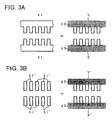
- Figs. 3A and 3B illustrate laminar structures of the electrode pair.
- the sustain electrodes X and Y having the above-described shape in a plan view can be formed by forming the electrically conductive transparent film 41 in a comb shape and putting the metal film 42 of the linear belt shape on the base portion of the comb shape, as shown in Fig. 3A.
- the width of the metal film 42 need not always be the same as the width of the base portion of the electrically conductive transparent film 41.
- the width of the metal film 42 can be selected to be the minimum width that can ensure a desired conductivity. Alternatively, as shown in Fig.
- the sustain electrodes X and Y can be formed by forming a required number of strips of electrically conductive film 41' in two lines and then putting the metal films 42 of the linear belt shape on each of the lines so that the metal films bridge the strips of the electrically conductive films 41'.
- the formation shown in Fig. 3A in which the metal film 42 is formed on a level plane (the upper surface of the electrically conductive transparent film 41) is more desirable than the formation shown in Fig. 3B in which the metal film needs to be formed to cover steps corresponding to the thickness of the electrically conductive transparent films 41', because the incidence of disconnection is lower in the case of Fig. 3A.
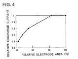
- Fig. 4 is a graph showing the relationship between the area of an electrode and the discharge current.
- a relative electrode area of 100% means a conventional structure in which the sustain electrodes X and Y are formed in belts having a constant width instead of the comb shape.
- the discharge current can be reduced without changing the driving voltage.
- the proportion of the area of the teeth X12 and Y12 per unit area is reduced by narrowing the widths of the teeth X12 and Y12 or by enlarging the arrangement pitch Ps, the discharge current becomes smaller.
- the sustain electrodes X and Y is covered with the dielectric layer 17 and thus a field distribution related to surface discharge does not completely agree with the shape of the electrodes, the effective electrode density hardly changes and the discharge current cannot be sufficiently reduced unless the electrode area is reduced to some extent (to 80% in the example).
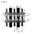
- Fig. 5 is a plan view illustrating a first modified structure of the electrode pair.
- the sustain electrodes X and Y are symmetrically formed.
- the sustain electrode X is formed in the shape of a comb comprised of a base portion X21 and teeth X22 and the sustain electrode Y is formed in the shape of a comb comprised of a base portion Y21 and teeth Y22.
- the arrangement pitch Ps of the teeth X22 of the sustain electrode X and the arrangement pitch Ps of the teeth Y22 of the sustain electrode Y are equal and 1/n (n is an integer) of the cell pitch Pr.
- the width in the row direction of the teeth Y22 of the sustain electrode Y which is also used as a scanning electrode is broader than the width in the row direction of the teeth X22 of the sustain electrode X.
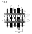
- Fig. 6 is a plan view illustrating a second modified structure of a pair of electrodes.
- the sustain electrode X is formed in the shape of a comb comprised of a base portion X31 and teeth X32 and the sustain electrode Y is formed in the shape of a comb comprised of a base portion Y31 and teeth Y32.
- the teeth X32 of the sustain electrode X and the teeth Y32 of the sustain electrode Y are the same in shape and size.
- the arrangement pitch Psy of the teeth Y32 of the sustain electrode Y is smaller than the arrangement pitch Psx of the teeth X32 of the sustain electrode X.
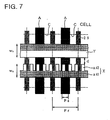
- Fig. 7 is a plan view illustrating a third modified structure of a pair of electrodes.
- the sustain electrode X is formed in the shape of a comb comprised of a base portion X41 and teeth X42.
- the sustain electrode Y is formed in the shape of a linear belt having a constant width Wy as in the conventional structure. Since the opposing area of sustain electrode Y with respect to the address electrode A is large, the addressing reliability is high.
- the discharge current is smaller than in the conventional PDP.
- the arrangement pitches Ps, Psx and Psy are selected to be 1/n (n is an integer) of the cell pitch Pr, the assembly is easy. More particularly, in the assembly of the front substrate structure and the rear substrate structure, the teeth are equally arranged in every cell C even if mis-alignment in the row direction occurs.
- the cell pitch Pr is selected to be more than twice as large as the arrangement pitches Ps, Psx and Psy, at least one tooth X12, y12, X22, Y22, X32, Y32 or X42 will exist between adjacent ribs 29 even if misalignment in the row direction occurs. This contributes to reliable surface discharges.
- the shape of the teeth X12, y12, X22, Y22, X32, Y32 and X42 is rectangular, but the shape thereof is not limited thereto.
- the teeth may be formed in a tapered trapezoid, for example.
- a central portion in the direction of extension may be enlarged so that the area thereof facing the address electrode A is increased.
- the invention is also applicable to PDPs of the projection type.
- the sustain electrodes X and Y may be made only of metal material.
- the invention is also applicable not only to PDPs in which the inverse slit width is larger than the slit width (the surface discharge gap d) so that discharge coupling in the row direction is prevented, but also to PDPs in which the sustain electrodes X and Y are all arranged equidistantly.
- the sustain electrodes X and Y may be formed in the shape of a double-toothed comb having teeth on both sides of a base portion.
- the discharge current can be set independently of the driving voltage. Further, the assembly of the devices is easy and the productivity can be maintained at the same level as that of conventional PDPs.
- the block-off of light by the electrodes can be kept to the minimum, and the disconnection of the metal film, which serves as the auxiliary conductor for reducing the resistance of the electrode, can be prevented.
Abstract
Description
- The present invention relates to a plasma display panel (PDP) of surface discharge structure.
- PDPs are now attracting much attention as display devices for high definition TV. For higher definition and up-sizing of screens of the PDPs, reduction of power consumption is one of the most significant challenges.
- AC-driven PDPs of surface discharge type are now commercially available as color display devices. Here, the surface discharge type means a type in which pairs of first and second main electrodes are arranged in parallel on an inner surface of one of a pair of substrates, and the first and the second main electrodes serve as positive electrodes and as negative electrodes alternately in an AC drive for sustaining a light emission state by use of wall charges. In surface discharge PDPs, fluorescent layers for color display can be provided on a substrate facing the substrate on which the main electrode pairs are placed, and thereby it is possible to prevent the fluorescent layers from being deteriorated by ion impact at electric discharges and to increase the life of the panel. A PDP having the fluorescent layers on a rear substrate is called a "reflection type," and one having fluorescent layers on a front substrate is called a "projection type." The reflection type, in which a front-side surface of the fluorescent layers emit light, is superior in luminous efficiency.
- Conventionally, the main electrodes are formed in the shape of linear belts (strips) of constant width extending in a direction of rows (in a direction of display lines) within a display region. The main electrodes are usually spaced in such a manner that the space between adjacent main electrode pairs (an inverse slit width) is sufficiently larger than the space between main electrodes that make a pair (a slit width), for the purpose of preventing discharge coupling between adjacent rows. However, it is also possible to adopt a configuration in which the main electrodes are regularly spaced and each main electrode forms pairs with main electrodes adjacent on either side. Additionally, the main electrode of the reflection type is comprised of an electrically conductive transparent film and a metal film for reducing line resistance.
- In the above-described surface discharge PDPs, the slit width which is a surface discharge gap and the width of the main electrodes determine a driving voltage margin. Here, the driving voltage margin means a range of driving voltages which allows stable display to be realized by use of a memory function of a dielectric, and is a difference between a firing voltage Vf and a sustain voltage Vs for sustaining electric discharges. A memory coefficient αM representative of the magnitude of the memory function is defined by the following formula:
- A larger memory coefficient αM brings greater stability and easier driving. Therefore, in designing a PDP, it is desirable to adopt as low a firing voltage Vf as possible to allow driving at lower voltages and also to increase the memory coefficient by reducing the sustain voltage Vs.
- Once dimensional conditions of the main electrodes and the driving voltage are determined, the magnitude of discharge current is uniquely determined. The magnitude of discharge current can be controlled by adjusting the driving voltage within the driving voltage margin. However, since the adjustment range of the driving voltage becomes narrower as the panel deteriorates with age, satisfactory control is practically impossible.
- A larger discharge current leads to a higher luminance. At the same time, however, the increase of luminance becomes slow in consequence of ultra violet light absorption by a discharge current. As a result, the luminous efficiency (ratio of luminance to power consumption) declines. In addition, since a larger discharge current results in a larger damage to inner surfaces owing to ion impact, the discharge current must be reduced as low as possible from the viewpoint of panel lifetime. To sum up, it is impossible to set the optimum driving voltage range and the optimum discharge current independently of each other in conventional PDPs. For determining cell structure and conditions of the discharge gas, a well-balanced drive voltage margin and discharge current must be set within a proper range through trial and error.
- An embodiment of the present invention may provide a plasma display panel which is adapted for setting a discharge current independently of a driving voltage, which is easy to assemble and excellent in productivity.
- The present invention provides a plasma display panel comprising a pair of substrates defining an electric discharge space therebetween; and electrodes extending in a row direction of the display to generate a surface discharge across a pair of the electrodes, wherein at least one electrode of the electrode pair for generating the surface discharge is formed in the shape of a comb having a base portion extending in the row direction and a tooth portion composed of a number of teeth extending from the base portion towards the other electrode, and an arrangement pitch of the teeth is 1/n of an arrangement pitch of cells in row direction of display, in which n is an integer more than or equal to two.
- Reference will now he made, by way of example only, to the accompanying drawings in which:-
- Fig. 1 is a perspective view illustrating the inner construction of a PDP embodying the present invention;
- Fig. 2 is a plan view illustrating a basic structure of a pair of electrodes in an embodiment of the present invention;
- Figs. 3A and 3B illustrate laminar structures of the pair of electrodes;
- Fig. 4 is a graph showing the relationship between the area of an electrode and discharge current;
- Fig. 5 is a plan view illustrating a first modified structure of electrodes; and
- Fig. 6 is a plan view illustrating a second modified structure of electrodes;
- Fig. 7 is a plan view illustrating a third modified structure of electrodes.
-
- In embodiments of the present invention, electrodes related to a surface discharge which extend in the row direction are in the form of comb teeth, and a discharge current is optimized by dimensions of the comb teeth (tooth portion). As the width of the comb teeth becomes narrower or the pitch between the comb teeth becomes larger, effective electrode density decreases and the discharge current declines.
- In addition to that, the pitch Ps of the comb teeth and the pitch Pr of cells meet a condition represented by the following formula:
- In the assembly of a PDP, a substrate on which the electrodes are arranged and another substrate are put together in alignment. Even if the substrates are mis-aligned in the row direction, the comb teeth will be placed in the same positions in all cells provided that the cell pitch Pr is an integer multiple of the comb teeth pitch Ps. If the comb teeth pitch Ps is half or less of the cell pitch Pr, at least one tooth is placed in every cell in the case of a PDP constructed to have ribs partitioning a discharge space for every cell. As a result, a surface discharge can be generated in all the cells. If the comb teeth pitch Ps is the same as cell pitch Pr, the comb teeth and the ribs may come into complete alignment by misalignment in the assembly and as a result, no comb teeth may be effective for the surface discharge. In other words, if the above-described pitch condition is satisfied, highly accurate alignment in the assembly of the substrates is not necessary. Accordingly, it is possible to keep the same productivity as in the case of a PDP provided with the conventional belt-shaped electrodes.
- One or both of the electrodes for the surface discharge which make a pair may be formed into the shape of a comb. In the case where both the electrodes are formed into the comb shape, the dimensions of the teeth may be the same, or may be different so that one of the electrodes which is used for addressing has a higher density than the other. In order to increase the electrode density, the width of each tooth may be broadened or the pitch of the teeth may be narrowed.
- In a plasma display panel embodying the present invention, each electrode of the electrode pair may be formed in the shape of a comb having a base portion extending in the row direction and a tooth portion comprised of a number of teeth extending from the base portion towards the other electrode, and a proportion of the tooth portion per unit area in one electrode of the electrode pair may be larger than that in the other electrode.
- Alternatively, or in addition, the arrangement pitch of the teeth in one electrode of the electrode pair may be larger than the arrangement pitch of the teeth in the other electrode.
- Each electrode of the electrode pair may be formed in the shape of a comb having a base portion extending in the row direction and a tooth portion comprised of a number of teeth extending from the base portion towards the other electrode, and the width of the teeth in one electrode of the electrode pair may be broader than the width of the teeth in the other electrode.
- One electrode of the electrode pair may be formed in the shape of a linear belt.
- Preferably, the base portion has a laminar structure of an electrically conductive transparent film and a metal film and the tooth portion is comprised of an electrically conductive transparent film which is made in one piece with the electrically conductive transparent film of the base portion.
- In a plasma display panel embodying the invention, the cells are defined by the respective electrode pairs in a discharge space partitioned by belt-shaped ribs extending in a direction of columns and crossing the electrode pairs.
- Referring now to Figure 1, a
PDP 1 embodying the invention is a PDP of the surface discharge type which is capable of color display. ThePDP 1 has a three electrode matrix structure in which sustain electrodes X and Y as a first and a second main electrode which make a pair intersect an address electrode A as a third electrode in each cell. The sustain electrodes X and Y extend in the row direction (in the horizontal direction) on a screen. One of the sustain electrodes, Y, is also used as a scanning electrode for selecting cells C row by row in addressing. The address electrode A extends in the column direction (in the vertical direction) on the screen and is used as a data electrode for selecting cells C column by column. - The
PDP 1 includes a pair of glass substrates which define adischarge space 30 therebetween. The sustain electrodes X and Y are arranged on an inner surface of the front one 11 of the pair of glass substrates in such a manner that one pair of sustain electrodes X and Y is on every row L. The row L is a line of cells in the horizontal direction on a screen. The sustain electrodes X and Y are each comprised of an electrically conductivetransparent film 41 and ametal film 42, and are covered with adielectric layer 17 for AC driving. Themetal film 42 serves as an auxiliary conductor for reducing line resistance value. The surface of thedielectric layer 17 is coated with aprotection film 18 of MgO. Thedielectric layer 17 and theMgO film 18 transmit light. A substrate having thereon constituents of cells, for example, a laminate of the sustain electrodes X and Y, thedielectric layer 17 and theprotection film 18, is called a substrate structure. On the rear one 21 of the pair of substrates, provided are abase layer 22, an address electrode A, aninsulation layer 24,ribs 29 andfluorescent layers ribs 29 is in the shape of a linear belt in a plan view. By theribs 29, thedischarge space 30 is partitioned in the row direction for each sub-pixel, and the spacing of thedischarge space 30 is defined at a fixed value (about 150 µm). Thedischarge space 30 is filled with a discharge gas containing a mixture of neon and a small amount of xenon. The fluorescent layers 28R, 28G and 28B are partially excited by ultra-violet rays generated by the surface discharge across the sustain electrodes X and Y, to emit visible color light . - One pixel for display is composed of three adjacent sub-pixels in the row direction. A structural unit within each sub-pixel is the cell C (see Fig. 2) Since the
ribs 29 are formed in a stripe pattern, a part of thedischarge space 30 which corresponds to each column is continuous in the column direction, bridging all the rows L. The sub-pixels on the same column emit light of the same color. The space between the electrodes of adjacent rows L (the inverse slit width) is broader than the surface discharge gap (the slit width). - The PDP1 with the above-described structure is produced by a series of steps of disposing the constituents separately on the
glass substrates transparent film 41, then depositing a metal thin film of three-layered structure of chromium-copper-chromium almost all over the surface of theglass substrate 11, and patterning the metal thin film by photolithography. - Fig. 2 is a plan view illustrating a basic structure of an electrode pair in accordance with the above embodiment.
- The sustain electrode X is formed in the shape of a comb comprised of a base portion X11 in the shape of a linear belt extending in the row direction to cover the whole width of the screen and a large number of teeth X12 arranged at regular intervals which extend from the base portion X11 towards the sustain electrode Y. The sustain electrode Y is also comprised of a base portion Y11 shaped in a linear belt and a large number of teeth Y12 spaced at regular intervals. The sustain electrodes X and Y are symmetrically placed. The width Wx of the sustain electrode X is the same as the width Wy of the sustain electrode Y, for example, about 150 to 250 µm. The surface discharge gap d is about 50 to 100 µm. The arrangement pitches Ps of the teeth X12 and Y12 are selected to be 1/n (n is an integer more than or equal to two) of the pitch Pr (about 660 µm) of the cells. That is to say, the pitches Ps and Pr satisfy the condition of
- Figs. 3A and 3B illustrate laminar structures of the electrode pair.
- The sustain electrodes X and Y having the above-described shape in a plan view can be formed by forming the electrically conductive
transparent film 41 in a comb shape and putting themetal film 42 of the linear belt shape on the base portion of the comb shape, as shown in Fig. 3A. In this case, the width of themetal film 42 need not always be the same as the width of the base portion of the electrically conductivetransparent film 41. The width of themetal film 42 can be selected to be the minimum width that can ensure a desired conductivity. Alternatively, as shown in Fig. 3B, the sustain electrodes X and Y can be formed by forming a required number of strips of electrically conductive film 41' in two lines and then putting themetal films 42 of the linear belt shape on each of the lines so that the metal films bridge the strips of the electrically conductive films 41'. However, the formation shown in Fig. 3A in which themetal film 42 is formed on a level plane (the upper surface of the electrically conductive transparent film 41) is more desirable than the formation shown in Fig. 3B in which the metal film needs to be formed to cover steps corresponding to the thickness of the electrically conductive transparent films 41', because the incidence of disconnection is lower in the case of Fig. 3A. - Fig. 4 is a graph showing the relationship between the area of an electrode and the discharge current. In Fig. 4, a relative electrode area of 100% means a conventional structure in which the sustain electrodes X and Y are formed in belts having a constant width instead of the comb shape.
- With the above-described comb-teeth construction of the electrode pairs for the surface discharge in which the teeth X12 and Y12 are opposite each other, the discharge current can be reduced without changing the driving voltage. As the proportion of the area of the teeth X12 and Y12 per unit area is reduced by narrowing the widths of the teeth X12 and Y12 or by enlarging the arrangement pitch Ps, the discharge current becomes smaller. In practice, however, since the sustain electrodes X and Y is covered with the
dielectric layer 17 and thus a field distribution related to surface discharge does not completely agree with the shape of the electrodes, the effective electrode density hardly changes and the discharge current cannot be sufficiently reduced unless the electrode area is reduced to some extent (to 80% in the example). - Fig. 5 is a plan view illustrating a first modified structure of the electrode pair.
- In the foregoing structure of the electrodes, the sustain electrodes X and Y are symmetrically formed. Also in an example shown in Fig. 5, the sustain electrode X is formed in the shape of a comb comprised of a base portion X21 and teeth X22 and the sustain electrode Y is formed in the shape of a comb comprised of a base portion Y21 and teeth Y22. The arrangement pitch Ps of the teeth X22 of the sustain electrode X and the arrangement pitch Ps of the teeth Y22 of the sustain electrode Y are equal and 1/n (n is an integer) of the cell pitch Pr. A feature of the example of Fig. 5 lies in that the width in the row direction of the teeth Y22 of the sustain electrode Y which is also used as a scanning electrode is broader than the width in the row direction of the teeth X22 of the sustain electrode X. With this construction, an opposing area of the sustain electrode Y with respect to the address electrode A is broader than that of the sustain electrode X and as a result, an address discharge is more easily generated. Thus, the discharge current can be reduced whilst maintaining addressing reliability.
- Fig. 6 is a plan view illustrating a second modified structure of a pair of electrodes.
- Also in the example of Fig. 6, the sustain electrode X is formed in the shape of a comb comprised of a base portion X31 and teeth X32 and the sustain electrode Y is formed in the shape of a comb comprised of a base portion Y31 and teeth Y32. The teeth X32 of the sustain electrode X and the teeth Y32 of the sustain electrode Y are the same in shape and size. However, the arrangement pitch Psy of the teeth Y32 of the sustain electrode Y is smaller than the arrangement pitch Psx of the teeth X32 of the sustain electrode X. With this construction, the opposing area of the sustain electrode Y with respect to the address electrode A is broader and therefore the addressing reliability is improved, as in the example of Fig. 5. Each of the arrangement pitches Psx and Psy is 1/n (n is an integer) of the cell pitch Pr.
- Fig. 7 is a plan view illustrating a third modified structure of a pair of electrodes.
- The sustain electrode X is formed in the shape of a comb comprised of a base portion X41 and teeth X42. On the other hand, the sustain electrode Y is formed in the shape of a linear belt having a constant width Wy as in the conventional structure. Since the opposing area of sustain electrode Y with respect to the address electrode A is large, the addressing reliability is high.
- In the electrode structures of the above-described examples, since one or both of the sustain electrodes X and Y is/are in the comb shape, the discharge current is smaller than in the conventional PDP. In addition to that, since the arrangement pitches Ps, Psx and Psy are selected to be 1/n (n is an integer) of the cell pitch Pr, the assembly is easy. More particularly, in the assembly of the front substrate structure and the rear substrate structure, the teeth are equally arranged in every cell C even if mis-alignment in the row direction occurs. Further, since the cell pitch Pr is selected to be more than twice as large as the arrangement pitches Ps, Psx and Psy, at least one tooth X12, y12, X22, Y22, X32, Y32 or X42 will exist between
adjacent ribs 29 even if misalignment in the row direction occurs. This contributes to reliable surface discharges. - In the above-described examples, the shape of the teeth X12, y12, X22, Y22, X32, Y32 and X42 is rectangular, but the shape thereof is not limited thereto. Alternatively, the teeth may be formed in a tapered trapezoid, for example. Particularly, as concerns the sustain electrode Y that is also used as the scanning electrode a central portion in the direction of extension may be enlarged so that the area thereof facing the address electrode A is increased.
- Though the present invention has been explained with a PDP of reflection type, the invention is also applicable to PDPs of the projection type. In the case of the projection type, the sustain electrodes X and Y may be made only of metal material. The invention is also applicable not only to PDPs in which the inverse slit width is larger than the slit width (the surface discharge gap d) so that discharge coupling in the row direction is prevented, but also to PDPs in which the sustain electrodes X and Y are all arranged equidistantly. In such a case, the sustain electrodes X and Y may be formed in the shape of a double-toothed comb having teeth on both sides of a base portion.
- By using the present invention, the discharge current can be set independently of the driving voltage. Further, the assembly of the devices is easy and the productivity can be maintained at the same level as that of conventional PDPs.
- Further, the addressing reliability can be ensured.
- Still further, in the case where the electrode pairs are disposed on the front substrate, the block-off of light by the electrodes can be kept to the minimum, and the disconnection of the metal film, which serves as the auxiliary conductor for reducing the resistance of the electrode, can be prevented.
Claims (10)
- A plasma display panel comprising:a pair of substrates defining an electric discharge space therebetween; andelectrodes extending in a row direction of the display to generate a surface discharge across a pair of the electrodes,
wherein at least one electrode of the electrode pair for generating the surface discharge is formed in the shape of a comb having a base portion extending in row direction of display and a tooth portion composed of a number of teeth extending from the base portion towards the other electrode, andan arrangement pitch of the teeth is 1/n of an arrangement pitch of cells in the row direction, in which n is an integer more than or equal to two. - A plasma display panel according to claim 1, wherein each electrode of the electrode pair is formed in the shape of a comb.
- A plasma display panel according to claim 2, wherein a proportion of the tooth portion per unit area in one electrode of the electrode pair is larger than that in the other electrode.
- A plasma display panel according to claim 2 or 3, wherein the arrangement pitches of the teeth of the electrode pair are the same.
- A plasma display panel according to claim 4, wherein the electrode pairs are symmetrically formed.
- A plasma display panel according to claim 4 or 5, wherein the width of the teeth of one electrode of the electrode pair is broader than the width of the teeth of the other electrode.
- A plasma display panel according to claim 2 or 3, wherein the arrangement pitch of the teeth of one electrode of the electrode pair is larger than the arrangement pitch of the teeth of the other electrode.
- A plasma display panel according to claim 1, wherein one electrode of the electrode pair is formed in the shape of a linear belt.
- A plasma display panel according to any one of the preceding claims, wherein the base portion in the comb comprises a laminate of an electrically conductive transparent film and a metal film, and the tooth portion is composed of an electrically conductive transparent film which is made in one piece with the electrically conductive transparent film of the base portion.
- A plasma display panel according to any one of the preceding claims, wherein the cells are each defined by each electrode pair within a discharge space partitioned by belt-shaped ribs extending in a direction of columns and crossing the electrode pairs.
Applications Claiming Priority (2)
| Application Number | Priority Date | Filing Date | Title |
|---|---|---|---|
| JP10011135A JPH11213894A (en) | 1998-01-23 | 1998-01-23 | Plasma display panel |
| JP1113598 | 1998-01-23 |
Publications (3)
| Publication Number | Publication Date |
|---|---|
| EP0932181A2 true EP0932181A2 (en) | 1999-07-28 |
| EP0932181A3 EP0932181A3 (en) | 1999-08-18 |
| EP0932181B1 EP0932181B1 (en) | 2003-11-12 |
Family
ID=11769589
Family Applications (1)
| Application Number | Title | Priority Date | Filing Date |
|---|---|---|---|
| EP98304641A Expired - Lifetime EP0932181B1 (en) | 1998-01-23 | 1998-06-11 | Plasma display panel |
Country Status (4)
| Country | Link |
|---|---|
| US (1) | US6157128A (en) |
| EP (1) | EP0932181B1 (en) |
| JP (1) | JPH11213894A (en) |
| KR (1) | KR100353465B1 (en) |
Cited By (3)
| Publication number | Priority date | Publication date | Assignee | Title |
|---|---|---|---|---|
| WO2001056052A1 (en) * | 2000-01-25 | 2001-08-02 | Matsushita Electric Industrial Co., Ltd. | Gas discharge panel |
| US6335592B1 (en) | 1998-10-28 | 2002-01-01 | Lg Electronics Inc. | Plasma display panel with specific electrode structures |
| EP1349192A2 (en) * | 2002-03-27 | 2003-10-01 | Fujitsu Hitachi Plasma Display Limited | Plasma display panel |
Families Citing this family (20)
| Publication number | Priority date | Publication date | Assignee | Title |
|---|---|---|---|---|
| US6445120B1 (en) * | 1998-10-28 | 2002-09-03 | Lg Electronics Inc. | Plasma display panel with improved structure of discharge electrode and dielectric layer |
| US6680573B1 (en) * | 1999-07-26 | 2004-01-20 | Lg Electronics Inc. | Plasma display panel with improved illuminance |
| JP4713717B2 (en) * | 1999-09-07 | 2011-06-29 | エルジー エレクトロニクス インコーポレイティド | Electrode structure of plasma display panel and sustain electrode driving method |
| JP3576051B2 (en) * | 1999-10-28 | 2004-10-13 | 富士通株式会社 | Plasma display panel and driving method thereof |
| KR100467688B1 (en) * | 2000-03-29 | 2005-01-24 | 삼성에스디아이 주식회사 | Plasma display panel |
| JP2002056781A (en) * | 2000-05-31 | 2002-02-22 | Mitsubishi Electric Corp | Plasma display panel and plasma display equipment |
| JP2002163986A (en) * | 2000-11-28 | 2002-06-07 | Nec Corp | Plasma display panel |
| JP2003007216A (en) * | 2001-06-25 | 2003-01-10 | Nec Corp | Plasma display panel and manufacturing method therefor |
| JP2003132798A (en) * | 2001-10-29 | 2003-05-09 | Nec Corp | Plasma display panel |
| KR100477994B1 (en) * | 2003-03-18 | 2005-03-23 | 삼성에스디아이 주식회사 | Plasma display panel and driving method thereof |
| KR100528926B1 (en) * | 2003-09-25 | 2005-11-15 | 삼성에스디아이 주식회사 | Plasma dispaly panel |
| KR100645278B1 (en) * | 2003-09-29 | 2006-11-15 | 파이오니아 가부시키가이샤 | Plasma display panel and plasma display device |
| US20070029908A1 (en) * | 2003-10-30 | 2007-02-08 | Masashi Goto | Plasma display panel |
| JP5062962B2 (en) * | 2004-03-24 | 2012-10-31 | パナソニック株式会社 | Plasma display panel |
| KR20050111906A (en) * | 2004-05-24 | 2005-11-29 | 삼성에스디아이 주식회사 | Plasma display panel |
| KR100673437B1 (en) * | 2004-12-31 | 2007-01-24 | 엘지전자 주식회사 | Plasma display panel |
| KR100737179B1 (en) * | 2005-09-13 | 2007-07-10 | 엘지전자 주식회사 | Plasma Display Panel |
| KR20070105136A (en) * | 2006-04-25 | 2007-10-30 | 삼성에스디아이 주식회사 | Plasma display panel |
| JPWO2011096176A1 (en) * | 2010-02-08 | 2013-06-10 | パナソニック株式会社 | Plasma display panel |
| JPWO2012102013A1 (en) * | 2011-01-28 | 2014-06-30 | パナソニック株式会社 | Plasma display panel |
Citations (3)
| Publication number | Priority date | Publication date | Assignee | Title |
|---|---|---|---|---|
| EP0680067A2 (en) * | 1994-04-28 | 1995-11-02 | Matsushita Electronics Corporation | Gas discharge display apparatus and method for driving the same |
| US5640068A (en) * | 1994-07-08 | 1997-06-17 | Pioneer Electronic Corporation | Surface discharge plasma display |
| EP0782167A2 (en) * | 1995-12-28 | 1997-07-02 | Pioneer Electronic Corporation | Surface discharge AC plasma display apparatus and driving method therefor |
Family Cites Families (2)
| Publication number | Priority date | Publication date | Assignee | Title |
|---|---|---|---|---|
| US29629A (en) * | 1860-08-14 | Improvement in plows | ||
| JPH10247474A (en) * | 1997-01-06 | 1998-09-14 | Sony Corp | Planar illuminating lamp and manufacture therefor |
-
1998
- 1998-01-23 JP JP10011135A patent/JPH11213894A/en active Pending
- 1998-06-11 EP EP98304641A patent/EP0932181B1/en not_active Expired - Lifetime
- 1998-06-12 US US09/096,569 patent/US6157128A/en not_active Expired - Fee Related
- 1998-07-02 KR KR10-1998-0026575A patent/KR100353465B1/en not_active IP Right Cessation
Patent Citations (3)
| Publication number | Priority date | Publication date | Assignee | Title |
|---|---|---|---|---|
| EP0680067A2 (en) * | 1994-04-28 | 1995-11-02 | Matsushita Electronics Corporation | Gas discharge display apparatus and method for driving the same |
| US5640068A (en) * | 1994-07-08 | 1997-06-17 | Pioneer Electronic Corporation | Surface discharge plasma display |
| EP0782167A2 (en) * | 1995-12-28 | 1997-07-02 | Pioneer Electronic Corporation | Surface discharge AC plasma display apparatus and driving method therefor |
Cited By (5)
| Publication number | Priority date | Publication date | Assignee | Title |
|---|---|---|---|---|
| US6335592B1 (en) | 1998-10-28 | 2002-01-01 | Lg Electronics Inc. | Plasma display panel with specific electrode structures |
| WO2001056052A1 (en) * | 2000-01-25 | 2001-08-02 | Matsushita Electric Industrial Co., Ltd. | Gas discharge panel |
| US6707259B2 (en) | 2000-01-25 | 2004-03-16 | Matsushita Electric Industrial Co., Ltd. | Gas discharge panel |
| EP1349192A2 (en) * | 2002-03-27 | 2003-10-01 | Fujitsu Hitachi Plasma Display Limited | Plasma display panel |
| EP1349192A3 (en) * | 2002-03-27 | 2005-08-17 | Fujitsu Hitachi Plasma Display Limited | Plasma display panel |
Also Published As
| Publication number | Publication date |
|---|---|
| KR19990066710A (en) | 1999-08-16 |
| EP0932181B1 (en) | 2003-11-12 |
| US6157128A (en) | 2000-12-05 |
| JPH11213894A (en) | 1999-08-06 |
| KR100353465B1 (en) | 2003-02-05 |
| EP0932181A3 (en) | 1999-08-18 |
Similar Documents
| Publication | Publication Date | Title |
|---|---|---|
| EP0932181B1 (en) | Plasma display panel | |
| JP3864204B2 (en) | Plasma display panel | |
| JP3445954B2 (en) | Plasma display panel | |
| EP1313124B1 (en) | Plasma display panel | |
| US6714175B1 (en) | Plasma display panel and method for driving the panel | |
| US6703782B2 (en) | Plasma display panel | |
| JP3909502B2 (en) | Gas discharge display panel | |
| KR20050045513A (en) | Plasma display panel | |
| KR100589369B1 (en) | Plasma display panel | |
| US7375467B2 (en) | Plasma display panel having stepped electrode structure | |
| US7378795B2 (en) | Plasma display panel | |
| US20060290279A1 (en) | Plasma display panel | |
| EP1696456B1 (en) | Plasma display apparatus | |
| US7663308B2 (en) | Plasma display panel | |
| US7629747B2 (en) | Plasma display panel having specific electrode structure | |
| US20070152595A1 (en) | Plasma display panel | |
| KR100659079B1 (en) | Plasma display panel | |
| KR100669329B1 (en) | Plasma display panel | |
| KR100683781B1 (en) | Plasma display panel | |
| KR100521478B1 (en) | Plasma display panel | |
| KR100570646B1 (en) | Plasma display panel | |
| KR100570695B1 (en) | Plasma display panel | |
| US20050052132A1 (en) | Plasma display panel | |
| US20070132385A1 (en) | Plasma display panel | |
| KR20050079428A (en) | Plasma display panel |
Legal Events
| Date | Code | Title | Description |
|---|---|---|---|
| PUAI | Public reference made under article 153(3) epc to a published international application that has entered the european phase |
Free format text: ORIGINAL CODE: 0009012 |
|
| PUAL | Search report despatched |
Free format text: ORIGINAL CODE: 0009013 |
|
| AK | Designated contracting states |
Kind code of ref document: A2 Designated state(s): DE FR GB NL |
|
| AX | Request for extension of the european patent |
Free format text: AL;LT;LV;MK;RO;SI |
|
| AK | Designated contracting states |
Kind code of ref document: A3 Designated state(s): AT BE CH CY DE DK ES FI FR GB GR IE IT LI LU MC NL PT SE |
|
| AX | Request for extension of the european patent |
Free format text: AL;LT;LV;MK;RO;SI |
|
| 17P | Request for examination filed |
Effective date: 19991027 |
|
| AKX | Designation fees paid |
Free format text: DE FR GB NL |
|
| 17Q | First examination report despatched |
Effective date: 20020813 |
|
| GRAH | Despatch of communication of intention to grant a patent |
Free format text: ORIGINAL CODE: EPIDOS IGRA |
|
| GRAS | Grant fee paid |
Free format text: ORIGINAL CODE: EPIDOSNIGR3 |
|
| GRAA | (expected) grant |
Free format text: ORIGINAL CODE: 0009210 |
|
| RBV | Designated contracting states (corrected) |
Designated state(s): FR NL |
|
| AK | Designated contracting states |
Kind code of ref document: B1 Designated state(s): FR NL |
|
| REG | Reference to a national code |
Ref country code: DE Ref legal event code: 8566 |
|
| ET | Fr: translation filed | ||
| PLBE | No opposition filed within time limit |
Free format text: ORIGINAL CODE: 0009261 |
|
| STAA | Information on the status of an ep patent application or granted ep patent |
Free format text: STATUS: NO OPPOSITION FILED WITHIN TIME LIMIT |
|
| 26N | No opposition filed |
Effective date: 20040813 |
|
| NLS | Nl: assignments of ep-patents |
Owner name: HITACHI, LTD. Effective date: 20051206 |
|
| REG | Reference to a national code |
Ref country code: FR Ref legal event code: TP |
|
| NLS | Nl: assignments of ep-patents |
Owner name: HITACHI PLASMA PATENT LICENSING CO., LTD. Effective date: 20070223 |
|
| REG | Reference to a national code |
Ref country code: FR Ref legal event code: TP |
|
| PGFP | Annual fee paid to national office [announced via postgrant information from national office to epo] |
Ref country code: NL Payment date: 20090615 Year of fee payment: 12 |
|
| REG | Reference to a national code |
Ref country code: NL Ref legal event code: V1 Effective date: 20110101 |
|
| REG | Reference to a national code |
Ref country code: FR Ref legal event code: ST Effective date: 20110228 |
|
| PG25 | Lapsed in a contracting state [announced via postgrant information from national office to epo] |
Ref country code: NL Free format text: LAPSE BECAUSE OF NON-PAYMENT OF DUE FEES Effective date: 20110101 Ref country code: FR Free format text: LAPSE BECAUSE OF NON-PAYMENT OF DUE FEES Effective date: 20100630 |
|
| PGFP | Annual fee paid to national office [announced via postgrant information from national office to epo] |
Ref country code: FR Payment date: 20090611 Year of fee payment: 12 |