EP0929836B1 - Procede pour produire un corps fa onne separateur de faisceaux et utilisation de ce dernier dans un module optoelectronique - Google Patents
Procede pour produire un corps fa onne separateur de faisceaux et utilisation de ce dernier dans un module optoelectronique Download PDFInfo
- Publication number
- EP0929836B1 EP0929836B1 EP97912015A EP97912015A EP0929836B1 EP 0929836 B1 EP0929836 B1 EP 0929836B1 EP 97912015 A EP97912015 A EP 97912015A EP 97912015 A EP97912015 A EP 97912015A EP 0929836 B1 EP0929836 B1 EP 0929836B1
- Authority
- EP
- European Patent Office
- Prior art keywords
- radiation
- beam splitter
- lateral surface
- wafer
- splitter layer
- Prior art date
- Legal status (The legal status is an assumption and is not a legal conclusion. Google has not performed a legal analysis and makes no representation as to the accuracy of the status listed.)
- Expired - Lifetime
Links
Images


Classifications
-
- G—PHYSICS
- G02—OPTICS
- G02B—OPTICAL ELEMENTS, SYSTEMS OR APPARATUS
- G02B27/00—Optical systems or apparatus not provided for by any of the groups G02B1/00 - G02B26/00, G02B30/00
- G02B27/10—Beam splitting or combining systems
- G02B27/1073—Beam splitting or combining systems characterized by manufacturing or alignment methods
-
- G—PHYSICS
- G02—OPTICS
- G02B—OPTICAL ELEMENTS, SYSTEMS OR APPARATUS
- G02B27/00—Optical systems or apparatus not provided for by any of the groups G02B1/00 - G02B26/00, G02B30/00
- G02B27/10—Beam splitting or combining systems
- G02B27/1006—Beam splitting or combining systems for splitting or combining different wavelengths
-
- G—PHYSICS
- G02—OPTICS
- G02B—OPTICAL ELEMENTS, SYSTEMS OR APPARATUS
- G02B6/00—Light guides; Structural details of arrangements comprising light guides and other optical elements, e.g. couplings
- G02B6/24—Coupling light guides
- G02B6/42—Coupling light guides with opto-electronic elements
- G02B6/4201—Packages, e.g. shape, construction, internal or external details
- G02B6/4246—Bidirectionally operating package structures
-
- G—PHYSICS
- G02—OPTICS
- G02B—OPTICAL ELEMENTS, SYSTEMS OR APPARATUS
- G02B6/00—Light guides; Structural details of arrangements comprising light guides and other optical elements, e.g. couplings
- G02B6/10—Light guides; Structural details of arrangements comprising light guides and other optical elements, e.g. couplings of the optical waveguide type
- G02B6/12—Light guides; Structural details of arrangements comprising light guides and other optical elements, e.g. couplings of the optical waveguide type of the integrated circuit kind
- G02B2006/12083—Constructional arrangements
- G02B2006/12114—Prism
-
- G—PHYSICS
- G02—OPTICS
- G02B—OPTICAL ELEMENTS, SYSTEMS OR APPARATUS
- G02B6/00—Light guides; Structural details of arrangements comprising light guides and other optical elements, e.g. couplings
- G02B6/24—Coupling light guides
- G02B6/42—Coupling light guides with opto-electronic elements
- G02B6/4201—Packages, e.g. shape, construction, internal or external details
- G02B6/4204—Packages, e.g. shape, construction, internal or external details the coupling comprising intermediate optical elements, e.g. lenses, holograms
- G02B6/4214—Packages, e.g. shape, construction, internal or external details the coupling comprising intermediate optical elements, e.g. lenses, holograms the intermediate optical element having redirecting reflective means, e.g. mirrors, prisms for deflecting the radiation from horizontal to down- or upward direction toward a device
-
- Y—GENERAL TAGGING OF NEW TECHNOLOGICAL DEVELOPMENTS; GENERAL TAGGING OF CROSS-SECTIONAL TECHNOLOGIES SPANNING OVER SEVERAL SECTIONS OF THE IPC; TECHNICAL SUBJECTS COVERED BY FORMER USPC CROSS-REFERENCE ART COLLECTIONS [XRACs] AND DIGESTS
- Y10—TECHNICAL SUBJECTS COVERED BY FORMER USPC
- Y10S—TECHNICAL SUBJECTS COVERED BY FORMER USPC CROSS-REFERENCE ART COLLECTIONS [XRACs] AND DIGESTS
- Y10S359/00—Optical: systems and elements
- Y10S359/90—Methods
Definitions
- the invention relates to a method for manufacturing a beam splitter shaped body according to the preamble of the claim 1.
- Such shaped beam splitter, z. B. prism cubes known.
- the known manufacturing processes for such prism cubes are very complex and therefore expensive.
- For the production of inexpensive optoelectronic components is so far the use of prism cubes not provided.
- EP-A-359 658 describes a process for the production of known several beam splitter bodies. The production takes place by sawing with conventional means at an angle to one Arrangement of several stacked disks.
- the invention has for its object a method for Develop production of beam splitter moldings that has as few technically complex process steps as possible.
- Figure 1 is a schematic representation of the flow of an embodiment the first method according to the invention
- Figure 2 is a schematic representation of the sequence of an embodiment the second method according to the invention
- Figure 3 is a schematic sectional view of a first optoelectronic Module with a according to the invention Process produced beam splitter body
- Figure 4 is a schematic sectional view of a second optoelectronic Module with a according to the invention Process produced beam splitter moldings
- Figure 5 is a schematic representation for explaining a Process sequence for the simultaneous production of a plurality of optoelectronic modules according to FIG. 3.
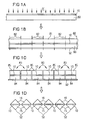
- a beam splitter layer 10 is applied.
- This beam splitter layer 10 can, for example, a 3dB divider layer or a WDM (wavelength division multiplex) filter layer be the z. B. as a short wave pass, long wave pass or attenuation filter is trained.
- the application of the beam splitter layer 10 is indicated in partial image A of FIG. 1 by arrows 91.
- the following (partial image B) is the beam splitter layer 10 a second radiation-permeable pane 81 is applied, which are made of quartz, borosilicate glass, sapphire, Si, GaP or from another suitable semiconductor material consists. This is z. B. by means of an adhesive (e.g. thermoset: epoxy resin, silicone rubber) on the beam splitter layer 10 attached.
- an adhesive e.g. thermoset: epoxy resin, silicone rubber
- the second disk 81 facing surface of the beam splitter layer 10 is a silicon layer (e.g. ⁇ -silicon) and the second disk 81 Glass, so these two components can be anodized Bonding.
- the two surfaces to be joined on top of each other for example heated to about 450 ° C, and opposite the glass the silicon has a voltage of, for example, -1000 V. created.
- Each of these Bars 83 consists of a first disc strip 84, one Beam splitter layer 10 and a second disc strip 85 (see drawing C).
- the rods 83 By grinding and / or polishing the side surfaces of the first and second disc strip 84.85 is then the Cross-sectional area lying perpendicular to the beam splitter layer 10 the rods 83 into the desired shape, e.g. B. hexagon, Rectangle or square. Then there are, for example so-called prism bars 52, which consist of a first prism 15 and a second prism 16 and one arranged between them Beam splitter layer 10 exist. These can then for example as shown in Figure 5 are processed or by sawing to their final length immediately brought and then further processed.
- the side surfaces of the prisms 15, 16, for example by means of ion plating or hydrothermal deposition etc. coated with an anti-reflective material.
- the method shown in Figure 2 differs from the aforementioned method in particular in that after Glue the composite onto the adhesive film 92 (partial image B) that on the opposite side of the beam splitter layer 10 arranged disc 81 by means of a saw blade 86 with a V-shaped sectional profile 87 with adjacent first V-grooves 93 is provided (partial image C).
- the first V-grooves 93 extend into the beam splitter layer 10.
- the composite z. B. by means of wax 94 on a carrier plate 88 attached so that the first V-grooves 93 provided side of the composite of the carrier plate is. Is located between the carrier plate 88 and the composite a paper layer, for example, on the carrier plate 88 95.
- the disk 80 becomes precise in the middle of the first V-grooves also using a Saw blade 86 with a V-shaped cutting profile 87 with adjoining provided second V-grooves 99, which are also in reach into the beam splitter layer 10 and cut through it.
- a Saw blade 86 with a V-shaped cutting profile 87 with adjoining provided second V-grooves 99, which are also in reach into the beam splitter layer 10 and cut through it.
- prism bars 52 which are essentially the valid form of the perpendicular to the beam splitter layer 10 lying cross-sectional area of the intended Have shaped beam splitter.
- the prism bars 52 for further process steps in one orderly bond, they are still on the Carrier plate 88 fixed prism bars 52, for example attached to a holding rod 97 by means of an epoxy resin 96 (Drawing file E).
- the composite is then removed from the carrier plate 88 detached so that a plurality of attached to the support rod 97 individual prism bars 52 is formed.
- This can then be further processed, e.g. B. means Cutting the prism bars 52 into prism cubes or Prism blocks or, as shown in Figure 5, application a substrate wafer for the production of optoelectronic Modules.
- a particular advantage of the invention described above is that several beam splitter moldings with any Cross-sectional area in the composite pane, d. H. in use. can be produced.
- the side faces of the prisms 15, 16 can also be used here for example by ion plating or hydrothermal deposition etc. coated with an anti-reflective material.
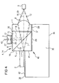
- the optoelectronic module of FIG. 3 is connected to a first one Main surface 30 of a carrier part 1 has a recess 31 and on one of the first main surface 30 opposite a second main surface 32 of the carrier part 1 a radiation focusing means 8 for focusing radiation, in this case a spherical converging lens.
- a radiation transparent Lanyard 29 e.g. B. a transparent adhesive, as beam splitter device 4, a beam splitter molded body, in in this case a prism cube 14 attached.
- the prism cube 14 consists of two assembled optical prisms 15, 16, between which the beam splitter layer 10 is arranged.
- the Beam splitter layer 10 lies on a diagonal plane of the Prism cube 14.
- this embodiment is not exclusively on the use of a prism cube 14 limited. It can also be used instead of the prism cube for example a square prism block or rectangular perpendicular to the beam splitter layer 10 lying cut surface can be used.
- connection means 33 between the transmission component 2 and the carrier part 1 is, for example, a solder or an adhesive is used.
- a solder or an adhesive is used as connection means 33 between the transmission component 2 and the carrier part 1 .
- connection means 33 between the transmission component 2 and the carrier part 1 is, for example, a solder or an adhesive is used.
- metallization layers 42 applied, which are connected to electrical connections of the transmission component 2 and are used as external electrical connections for serve the transmitter component 2.
- the transmission component 2 can do this directly with its electrical connections on the metallization layers 42 lie on and with them, for example be electrically connected by means of a solder.
- the transmission component beam exit surface 11 can be optional rest directly on the first side surface 5 of the prism cube or be arranged at a distance from it. in the second case, the space between the radiation exit surface 11 and the first side surface 5 of the prism cube 14, as shown in Figure 3, with a radiation transparent Coupling medium 24 be filled, its refractive index compared to that of air. This can result in loss of reflection due to very different refractive indices of air and semiconductor material or material of the prism cube be reduced. Ideally, the transmitter component faces the radiation exit area 11 to the first side surface 5 physical contact.
- the second Side surface 6 of the prism cube 14 is by means of a radiation-permeable connecting means 25 a receiving component 3, e.g. B. a photodiode attached.
- the receiving device beam entry surface 12 of the receiving device 3 faces the second side surface 6.
- the prism cube 14 is arranged such that the beam splitter layer 10 lies in a plane that is between the transmission component 2 and the receiving component 3 is arranged and the one with the first main surface 30 of the carrier part 1 Includes 45 ° angle.
- a connecting means 34 e.g. B. a metallic solder or an adhesive
- a monitor diode 21 attached on the opposite side of the transmission component 2 Prism cube 14 is also in the recess 31 of the support member 1 by means of a connecting means 34, e.g. B. a metallic solder or an adhesive, a monitor diode 21 attached.
- This monitor diode 21 essentially serves the radiation 7 emitted by the transmission component 2 onto it Check wavelength. This is the beam splitter layer 10 trained so that they emitted part of the Radiation 7 passes.
- the monitor diode 21 is arranged so that a monitor diode beam entry surface 23 one of the first side surface 5 opposite fourth side surface 22 of the prism cube 14 is facing.
- a space between the fourth Side surface 22 of the prism cube 14 and the monitor diode beam entry surface 23 is by means of a transparent Coupling medium 26, e.g. B. a transparent epoxy resin, filled. This in turn can cause reflection losses Radiation on the way to the monitor diode 21 can be reduced.
- One opposite the monitor diode beam entry surface 23 Side surface 44 of the monitor diode 21 is chamfered in such a way that they have at least part of that in the monitor diode 21 penetrating radiation to a radiation-detecting pn junction 45 of the monitor diode 21 is reflected. she closes with one closest to the pn junction 45 Side surface 46 of the monitor diode an angle that is smaller than 90 °. In addition, it can be used, for example, with a reflection-enhancing layer.
- the transmission component 2, the reception component 3, the prism cube 14, and the radiation focusing means 8 are such trained and arranged to each other that in the operation of the optotelectronic Module at least part of one of that Transmitting component 2 emitted radiation 7 after passage through the radiation focusing means 8 in a direction of propagation considered the emitted radiation 7, the Radiation focusing means 8 downstream optical device 9 is coupled in and that at least part of one of the optical device 9, received Radiation 13 after passing through the radiation focusing means 8 and through the prism cube 14 into the receiving component 3 is coupled.
- the prism cube 14 is made for one Radiation 7 and the received radiation 13 transparent material manufactured (e.g. quartz, borosilicate glass, sapphire or Semiconductor material (compare, for example, the semiconductor materials specified below for the carrier part)).
- the beam splitter layer 10 is designed such that it the emitted radiation 7 largely reflects and the received radiation 13 transmits as far as possible.
- Such Beam splitter layers 10 are in optical technology known, e.g. B. 3dB divider or WDM (wavelength division multiplex) filter, and are therefore at this point not explained in more detail. Is optional on the side surfaces 5,6,17,22 of the prism cube an anti-reflective coating 48 (shown in dashed lines) applied.
- the beam axis 19 of the radiation 7 emitted and the Beam axis 20 of the received radiation 13 are at this Execution example perpendicular to each other.
- the emitted radiation 7 and the received radiation 13 advantageously have different wavelengths ⁇ . This applies to all of the exemplary embodiments described in this application of the optoelectronic module according to the invention.
- the optical device 9 is, for example, as in the figure 3 indicated, an optical waveguide, a lens arrangement or another optoelectronic module etc.
- the carrier part 1 including the radiation focusing means 8 is made of a material that is also suitable for both emitted radiation 7 as well as for the received radiation 13 is permeable. Glass, for example, is suitable for this. Plastic, sapphire, diamond or a semiconductor material that for the emitted radiation 7 and for the received radiation 13 is permeable.
- a material that is also suitable for both emitted radiation 7 as well as for the received radiation 13 is permeable. Glass, for example, is suitable for this.
- For wavelengths ⁇ > 400 nm in this regard, for example SiC, for ⁇ > 550 nm GaP, for ⁇ > 900 nm GaAs and for ⁇ > 1100 nm silicon can be used.
- the radiation focusing means 8 can for example be a converging lens with a spherical or aspherical surface be produced by means of etching or grinding.
- a radiation focusing means 8 a diffractive optical Element, a holographic optical element or a Fresnel lens can be used by means of etching, grinding or milling.
- the recess 31 is for example made by etching or milling.
- the recess 31 can alternatively also be separated by means of two manufactured molded parts, which on the carrier part 1 with a Are attached to each other, be realized.
- the radiation focusing means 8 as an alternative to the above Described separately manufactured and on the support part 1 z. B. using a radiation-permeable solder or adhesive be attached. If the carrier part 1 consists for example of - Silicon and the radiation focusing means 8 made of glass, see above these two components can also be anodically bonded be connected.
- the active components of the optoelectronic Module d. H. the transmission component 2, the reception component 3, and the monitor diode 21 from environmental influences to protect, the entire functional unit, consisting from these three components and the prism cube 14 with one essentially made of plastic or of another potting material existing encapsulation, for example a Epoxy resin or another suitable plastic, cast his.
- the optoelectronic module according to the invention can also be used a hermetically sealed metal housing with an optical Have windows.
- the optoelectronic module shown in FIG. 4 differs differs from that according to FIG. 3 in particular in that the radiation focusing means 8 on the transmission component 2 opposite side of the prism cube 14 is arranged and that the beam splitter layer 10 is formed such that it largely transmits the emitted radiation 7 and that it largely reflects the received radiation 13.
- the beam axis 19 of the radiation 7 emitted and the Beam axis 20 of the received radiation 13 run parallel to each other, especially lie on each other.
- the Beam axis 43 of the reflected on the beam splitter layer 10 Part of the received radiation 13 is perpendicular the beam axis 19 of the received radiation 13.
- the transmission component 2, the prism cube 14 and the radiation focusing means 8 are for example by gluing or soldered onto a common carrier element 36, which essentially consists of silicon, for example.
- the Carrier element 36 has a step 40 which has a first mounting surface 37 and a second parallel to this Mounting surface 38 separates from each other.
- the prism cube 14 is adjacent on the first mounting surface 37 to a perpendicular to the mounting surfaces 37,38 Heel area 41 of level 40 attached. That about this The connecting means 29 used does not have to be transparent to radiation his.
- On the first mounting surface 37 is still means a connection means 28 the radiation focusing means 8 attached such that its radiation entry and Beam exit surface 18 parallel to the third side surface 17 of the prism cube 14 lies and this is facing.
- a gap which with a transparent coupling medium 26, for. B. synthetic resin, is filled.
- the radiation focusing means can of course also be used 8 have physical contact with the prism cube 14, in particular, directly concern this.
- the transmission component 2 is on the second mounting surface 38 attached such that its radiation exit surface 11 the Prism cube 14 is facing, and immediately on the first Side surface 5 is applied. Between the transmission component 2 and the prism cube 14 can of course be the same as that Embodiment of Figure 3, there should be a gap to reduce reflection with a transparent coupling medium 24, e.g. B. synthetic resin is filled, or a physical Contact.
- a transparent coupling medium 24 e.g. B. synthetic resin is filled, or a physical Contact.
- Metallization layers are on the second mounting surface 38 42 applied. These are with electrical contacts of the Transmitting device 2 electrically connected.
- the transmission component 2 and the metallization layers 42 designed such that electrical contacts of the Transmitting component 2 and the metallization layers 42 lie one on top of the other and for example by means of a metallic solder or by means of an electrically conductive adhesive are connected.
- the metallization layers 42 serve at the same time as external electrical connections for the Transmitting component 2, for example by means of bond wires are connected to a lead frame.
- the carrier part 1 corresponding metallization layers 42 may be provided.
- a blocking filter 27 is arranged, that for the wavelength of the emitted radiation 7 is largely impermeable. This can reduce crosstalk of the optoelectronic module can be reduced. Under "Crosstalk" is a direct transmission of that from the transmission component 2 emitted signals on the receiving component 3 to understand.
- the blocking filter 27 can optionally be on the receiving component radiation entry surface 12 or on the second Side surface 6 of the prism cube 14 may be applied.
- the receiving device beam entry surface 12 and the Prismatic cubes 14 can be arranged a converging lens.
- a laser diode is used as the transmission component 2, then these with the active side up (up-side up) or with the active zone down (up-side down), d. H. in the direction Carrier element 36 may be mounted.
- the thickness of the laser diode substrate very precisely to the position of the Beam splitter layer 10 may be adapted. This is with a high Assembly and adjustment effort connected.
- the thickness of the epitaxial layer of the laser diode goes and the thickness of any electrical connection metallization layers present 42 on the carrier element 36 in this consideration. Manufacturing tolerances can be found here be kept very simple in the micrometer range and below. The adjustment is significantly simplified. Analogue naturally also applies to the exemplary embodiment described above of Figure 3.
- a monitor diode 21 provided, this can be seen from the prism cube 14, behind the transmission component 2 on the second mounting surface 38 be arranged. Part of those generated in the transmission component 2 Radiation must then of course be coupled out to the rear, what with using a laser diode as a transmission component 2 a deterioration of the laser parameters is connected because the rear resonator mirror is also partially transparent have to be.
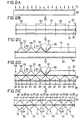
- the main surface 61 of the disk 50 is predetermined Raster a number of radiation focusing means 8 educated. In this case, these are e.g. B. by means of etching spherical or aspherical lenses.
- the radiation focusing means 8 are arranged in rows, which run parallel to the grooves 54 and this perpendicular opposite.
- the disc 50 consists of a for the emitted radiation 7 and the received radiation 13 permeable material. Compare the description to Figure 3.
- each groove 54 is adjacent to a first groove side surface 55 a prism bar 52 with a square cross section is attached.
- the first groove side surface 55 can be used as an adjustment reference surface for a first side surface 5 of the prism bar 52 serve.
- Each prism bar 52 has a beam splitter layer 10 on one to its longitudinal central axis parallel diagonal cut surface of the prism bar 52 lies. The angle a between the beam splitter layer 10 and the first main surface 51 of the disk 50 is thus 45 °.
- the prism bar 52 is made of glass and the Disk 50 made of ⁇ -silicon or vice versa, can be used for fastening the prism bar 52 on the disc 50 instead of connecting specified above by means of a connecting means 29 anodic bonding can be used.
- the surfaces to be connected are placed on top of each other, for example heated to about 450 ° C and between glass and - Silicon applied a voltage of approximately -1000 V.
- This connection technology is also possible, even if the disc 50 is made of glass or any other material and on an ⁇ -silicon layer at the connection point to the prism bar 52 having. It just needs a glass and an ⁇ -silicon layer lie on top of one another.
- the disk 50 is adjacent on the first main surface 51 a plurality of transmission components to the first side surfaces 5 2 attached, such that electrical contacts of the transmission components 2 on the designated on the first Main surface 51 of the disk 50 applied metallization layers 42 come to rest and are electrically conductive with them get connected.
- the side surface 5 serve as an adjustment reference surface for the transmission components 2.
- the transmission components 2 are arranged so that each one Radiation focusing means 8 is assigned.
- each assigned a radiation focusing means 8 is.
- Analogous to this, is adjacent to one of the first side surfaces 5 opposite fourth side surface 22, in the groove 54 a plurality of monitor diodes 21 with electrical Contacts 56 attached.
- laser diodes When using laser diodes as transmission components 2 can these by means of metallization tracks 57 (dashed lines in FIG. 5) shown) on the first main surface 51 of the Disk 50 are connected in series, so that for the so-called Burn-in the laser diodes only the two outer ones arranged at the two ends of individual laser diode lines 58 Contact surfaces 42 must be contacted.
- the Burn-in for the same laser diode row 58 assigned Laser diodes can thus be operated simultaneously in a particularly simple manner be performed.
- the individual transmit components 2 and 3 receive components Contacting the associated metallization layers 42, 56 and connection to a suitable wafer tester in the wafer assembly, in use, on their electro-optical parameters be measured. The same naturally applies to the monitor diodes 21.
- the disk 50 is then and the prism bars 52 along first dividing lines 59, between the individual transmission components 2 perpendicular to the grooves 54 run, and the disc 50 along second Dividing lines 60, which each run between two grooves 54, severed.
- Each manufactured a transmission component 2, a receiving component 3, a monitor diode 21, a prism block 14 and a radiation focusing means 8 with carrier part 1 having individual devices subsequently processed depending on the intended application, e.g. B. attached to a lead frame and with a Potting envelope 35 provided.
Landscapes
- Physics & Mathematics (AREA)
- General Physics & Mathematics (AREA)
- Optics & Photonics (AREA)
- Engineering & Computer Science (AREA)
- Manufacturing & Machinery (AREA)
- Optical Elements Other Than Lenses (AREA)
- Mechanical Treatment Of Semiconductor (AREA)
- Optical Integrated Circuits (AREA)
- Optical Couplings Of Light Guides (AREA)
Claims (13)
- Procédé de fabrication d'au moins un corps (14) façonné diviseur de faisceau, qui laisse passer le rayonnement électromagnétique et dans lequel est incorporée une couche (10) diviseuse de faisceau, caractérisé par les étapes suivantes :a) fabrication d'une première galette (80), constituée de matériau laissant passer le rayonnement,b) apposition de la couche (10) diviseuse de faisceau sur une face principale de la première galette (80),c) apposition d'une deuxième galette (81), constituée de matériau laissant passer le rayonnement, sur la couche (10) diviseuse de faisceau,d) sectionnement de la deuxième galette (81) et sciage de la couche (10) diviseuse de faisceau le long de lignes (82) de séparation s'étendant parallèlement entre elles, au moyen d'un outil à tronçonner à profil (87) de coupe en forme de V, de telle sorte qu'on obtient des premières bandes (84) de galette séparées les unes des autres,e) fixation sur une plaque (88) de support de l'assemblage comprenant la première galette (80), la deuxième galette (81) et la couche (10) diviseuse de faisceau, de telle sorte que les premières bandes (84) de galette sont tournées vers la plaque (88) de support,f) sectionnement de la première galette (80) et de la couche (10) diviseuse de faisceau le long de lignes (82) de séparation s'étendant parallèlement entre elles, au moyen d'un outil à tronçonner à profil (87) de coupe en forme de V, de telle sorte qu'on produit des deuxièmes bandes (85) de galette séparées les unes des autres, opposées aux premières bandes (84) de galette, et donc qu'on forme des barrettes (52) de corps façonné diviseur de faisceau, séparées les unes des autres, ayant la forme de section souhaitée du corps (14) façonné diviseur de faisceau, etg) sectionnement des barres (83) transversalement à leur axe longitudinal.
- Procédé suivant la revendication 1, caractérisé en ce qu'à la suite du sectionnement de la deuxième galette (81) et du sciage de la couche (10) diviseuse de faisceau, on ponce et/ou on polit les faces (89) de coupe des premières bandes (84) de galette, et en ce qu'à la suite du sectionnement de la première galette (80) et de la couche (10) diviseuse de faisceau, on ponce et/ou on polit les faces (90) de coupe des deuxièmes bandes (85) de galette.
- Procédé suivant la revendication 1 ou 2, caractérisé en ce que la couche (10) diviseuse de faisceau comporte une succession de couches utilisant la technologie WDM (Wavelength Division Multiplexing - multiplexage par division en longueurs d'onde).
- Procédé suivant l'une des revendications 1 à 3, caractérisé en ce qu'on utilise comme deuxième galette (81) une galette en verre, en ce qu'une couche partielle, limitrophe de la galette en verre, de la couche (10) diviseuse de faisceau est constituée de silicium, et en ce que la galette en verre est assemblée à la couche (10) diviseuse de faisceau par bonding anodique.
- Utilisation d'un corps (14) façonné diviseur de faisceau fabriqué suivant l'une des revendications 1 à 4 dans un module optoélectronique pour la transmission optique bidirectionnelle de données, caractérisée en ce qu'un composant (2) émetteur destiné à émettre un rayonnement, un composant (3) récepteur destiné à recevoir un rayonnement, un moyen (8) focalisateur de rayonnement destiné à focaliser un rayonnement et le corps (14) façonné diviseur de faisceau sont conçus et disposés les uns par rapport aux autres de telle sorte que, lorsque le module optoélectronique est en service, au moins une partie d'un rayonnement (7) émis par le composant (2) émetteur est injectée dans un dispositif (9) optique accouplé optiquement au module optoélectronique, et qu'au moins une partie d'un rayonnement (13) reçu, découplé du dispositif (9) optique, est injectée dans le composant (3) récepteur.
- Utilisation suivant la revendication 5, caractérisée en ce que le corps (14) façonné diviseur de faisceau a la forme d'un parallélépipède, en ce que la couche (10) diviseuse de faisceau se trouve dans un plan diagonal de section du parallélépipède, et en ce qu'un plan de section du parallélépipède perpendiculaire à la couche (10) diviseuse de faisceau a la forme d'un rectangle, notamment d'un carré.
- Utilisation suivant la revendication 5 ou 6, caractérisée en ce que le corps (14) façonné diviseur de faisceau comporte au moins une première face (5) latérale, une deuxième face (6) latérale et une troisième face (17) latérale,en ce que la première face (5) latérale et la deuxième face (6) latérale sont inclinées l'une par rapport à l'autre,en ce que la troisième face (17) latérale et la deuxième face (6) latérale ou la troisième face (17) latérale et la première face (5) latérale sont inclinées l'une par rapport à l'autre,en ce que la première face (5) latérale et la troisième face (17) latérale, ou respectivement la deuxième face (6) latérale et la troisième face (17) latérale, sont des faces latérales opposées du corps (14) façonné diviseur de faisceau,en ce qu'une face (11) de sortie de faisceau du composant (2) émetteur est tournée vers la première face (5) latérale,en ce qu'une face (12) d'entrée de faisceau du composant (3) récepteur est tournée vers la deuxième face (6) latérale,en ce qu'une face (18) d'entrée et de sortie de faisceau du moyen (8) focalisateur de rayonnement est tournée vers la troisième face (17) latérale,et en ce que la couche (10) diviseuse de faisceau est disposée de telle sorte qu'elle coupe tant l'axe (19) du rayonnement (7) émis que l'axe (20) du rayonnement (13) reçu.
- Utilisation suivant la revendication 7, caractérisée en ce que la première face (5) latérale et la deuxième face (6) latérale sont mutuellement perpendiculaires,en ce que la troisième face (17) latérale et la deuxième face (6) latérale ou la troisième face (17) latérale et la première face (5) latérale sont mutuellement perpendiculaires,en ce que la première face (5) latérale et la troisième face (17) latérale, ou respectivement la deuxième face (6) latérale et la troisième face (17) latérale, sont des faces latérales opposées mutuellement parallèles du corps (14) façonné diviseur de faisceau.
- Utilisation suivant la revendication 7 ou 8, caractérisée en ce que la face (11) de sortie de faisceau du composant (2) émetteur est assemblée à la première face (5) latérale, en ce que la face (12) d'entrée de faisceau du composant (3) récepteur est assemblée à la deuxième face (6) latérale, et en ce que la face (18) d'entrée et de sortie de faisceau du moyen (8) focalisateur de rayonnement est assemblée à la troisième face (17) latérale.
- Utilisation suivant l'une des revendications 5 à 9, caractérisée en ce que le moyen (8) focalisateur de rayonnement comporte une partie (1) de support, qui est assemblée au corps (14) façonné diviseur de faisceau au moyen d'un agent (29) de liaison laissant passer le rayonnement, en ce que la partie (1) de support est constituée pour l'essentiel d'un matériau laissant passer le rayonnement (7) émis et le rayonnement (13) reçu, et en ce que le composant (2) émetteur et le dispositif (9) optique sont disposés sur des côtés différents de la partie (1) de support.
- Utilisation suivant l'une des revendications 5 à 10, caractérisée en ce qu'il est prévu une diode (21) de contrôle, qui comporte une face (23) d'entrée de faisceau tournée vers une quatrième face (22) latérale du corps (14) façonné diviseur de faisceau, et en ce que la couche (10) diviseuse de faisceau est conçue pour laisser passer partiellement le rayonnement (7) émis de telle sorte qu'une première partie du rayonnement (7) émis rencontre la face (23) d'entrée de faisceau de la diode de contrôle.
- Utilisation suivant l'une des revendications 7 à 11, caractérisée en ce que l'axe (19) du rayonnement (7) émis et l'axe (20) du rayonnement (13) reçu s'étendent sensiblement parallèlement entre eux, en ce que la couche (10) diviseuse de faisceau est conçue et disposée de telle sorte qu'elle laisse passer une partie du rayonnement (7) émis à coupler dans le dispositif (9) optique et qu'elle réfléchit pour sa majeure partie le rayonnement (13) reçu et le dévie vers le composant (3) récepteur, et en ce que le moyen (8) focalisateur de rayonnement et le composant (2) émetteur sont disposés sur des côtés opposés du corps (14) façonné diviseur de faisceau,
ou en ce que l'axe (19) du rayonnement (7) émis et l'axe (20) du rayonnement (13) reçu forment entre eux un angle de 90°, et en ce que la couche (10) diviseuse de faisceau est conçue et disposée de telle sorte qu'elle réfléchit au moins pour sa majeure partie le rayonnement (7) émis, de sorte que l'axe du rayonnement réfléchi s'étend parallèlement à l'axe (20) du rayonnement (13) reçu, et qu'elle laisse passer au moins une partie du rayonnement (13) reçu, de sorte que ce dernier rencontre la face (12) d'entrée de faisceau du composant récepteur. - Utilisation suivant la revendication 8 ou suivant la revendication 8 et l'une des revendications 9 à 12, caractérisée en ce que l'axe (19) du rayonnement (7) émis et l'axe (20) du rayonnement (13) reçu s'étendent sensiblement parallèlement entre eux, en ce que la couche (10) diviseuse de faisceau est conçue et disposée de telle sorte qu'elle laisse passer une partie du rayonnement (7) émis à coupler dans le dispositif (9) optique et qu'elle réfléchit pour sa majeure partie le rayonnement (13) reçu et le dévie vers le composant (3) récepteur, et en ce que le moyen (8) focalisateur de rayonnement et le composant (2) émetteur sont disposés sur des côtés opposés du corps (14) façonné diviseur de faisceau,
ou en ce que l'axe (19) du rayonnement (7) émis et l'axe (20) du rayonnement (13) reçu forment entre eux un angle de 90°, et en ce que la couche (10) diviseuse de faisceau est conçue et disposée de telle sorte qu'elle réfléchit au moins pour sa majeure partie le rayonnement (7) émis, de sorte que l'axe du rayonnement réfléchi s'étend parallèlement à l'axe (20) du rayonnement (13) reçu, et qu'elle laisse passer au moins une partie du rayonnement (13) reçu, de sorte que ce dernier rencontre la face (12) d'entrée de faisceau du composant récepteur.
Applications Claiming Priority (3)
| Application Number | Priority Date | Filing Date | Title |
|---|---|---|---|
| DE19640236 | 1996-09-30 | ||
| DE19640236 | 1996-09-30 | ||
| PCT/DE1997/002201 WO1998014818A1 (fr) | 1996-09-30 | 1997-09-26 | Procede pour produire un corps façonne separateur de faisceaux et utilisation de ce dernier dans un module optoelectronique |
Publications (2)
| Publication Number | Publication Date |
|---|---|
| EP0929836A1 EP0929836A1 (fr) | 1999-07-21 |
| EP0929836B1 true EP0929836B1 (fr) | 2000-08-09 |
Family
ID=7807396
Family Applications (1)
| Application Number | Title | Priority Date | Filing Date |
|---|---|---|---|
| EP97912015A Expired - Lifetime EP0929836B1 (fr) | 1996-09-30 | 1997-09-26 | Procede pour produire un corps fa onne separateur de faisceaux et utilisation de ce dernier dans un module optoelectronique |
Country Status (7)
| Country | Link |
|---|---|
| US (1) | US6028708A (fr) |
| EP (1) | EP0929836B1 (fr) |
| JP (1) | JP2001501741A (fr) |
| CN (1) | CN1143155C (fr) |
| DE (1) | DE59702158D1 (fr) |
| TW (1) | TW349175B (fr) |
| WO (1) | WO1998014818A1 (fr) |
Cited By (1)
| Publication number | Priority date | Publication date | Assignee | Title |
|---|---|---|---|---|
| DE102011087846A1 (de) * | 2011-12-06 | 2013-06-06 | Schildtec GmbH | Verfahren zum Herstellen optischer Strahlteilerwürfel |
Families Citing this family (12)
| Publication number | Priority date | Publication date | Assignee | Title |
|---|---|---|---|---|
| US7157302B2 (en) * | 1998-06-04 | 2007-01-02 | Micron Technology, Inc. | Imaging device and method of manufacture |
| DE10013261B4 (de) * | 2000-03-17 | 2007-03-01 | Agilent Technologies, Inc. (n.d.Ges.d.Staates Delaware), Palo Alto | Mikromechanisch hergestellter optischer Strahlteiler |
| DE10037902C2 (de) * | 2000-08-03 | 2002-08-01 | Infineon Technologies Ag | Optisches bidirektionales Sende- und Empfangsmodul mit einem Stiftkörper mit integriertem WDM-Filter |
| US6900777B1 (en) * | 2001-01-03 | 2005-05-31 | Stryker Corporation | Infrared audio/video interface for head-mounted display |
| DE10125469B4 (de) | 2001-05-25 | 2008-01-10 | Leica Microsystems Cms Gmbh | Vorrichtung zur Ermittlung einer Lichtleistung, Mikroskop und Verfahren zur Mikroskopie |
| DE10319901A1 (de) * | 2003-04-29 | 2004-11-25 | Infineon Technologies Ag | Optische Anordnung mit mindestens einem Sendebauelement und einem dem Sendebauelement jeweils zugeordneten Monitorbauelement |
| JP2013061587A (ja) * | 2011-09-15 | 2013-04-04 | Alps Electric Co Ltd | ビームスプリッタ及びそれを用いた光通信モジュール |
| CN104428696B (zh) * | 2012-06-27 | 2019-01-18 | 3M创新有限公司 | 光学部件阵列 |
| DE102012221011B3 (de) * | 2012-11-16 | 2014-04-10 | Schildtec GmbH | Verfahren zum Herstellen optischer Strahlteilerwürfel |
| CN105829954B (zh) | 2013-12-23 | 2018-11-09 | 3M创新有限公司 | 集成光学部件及其制造方法 |
| US10313642B2 (en) * | 2017-01-18 | 2019-06-04 | Omnivision Technologies, Inc. | Imaging system having dual image sensors |
| JP6943660B2 (ja) * | 2017-07-14 | 2021-10-06 | 株式会社エンプラス | 光レセプタクルおよび光モジュール |
Family Cites Families (7)
| Publication number | Priority date | Publication date | Assignee | Title |
|---|---|---|---|---|
| CH651939A5 (en) * | 1979-08-27 | 1985-10-15 | Int Standard Electric Corp | Optical beam splitter |
| JPS59139003A (ja) * | 1983-01-31 | 1984-08-09 | Sony Corp | マイクロプリズム用原板の製造方法 |
| US4627688A (en) * | 1983-07-01 | 1986-12-09 | Sano Kiko Co., Ltd. | Beam splitter |
| US4732449A (en) * | 1985-10-25 | 1988-03-22 | G & H Technology | Beam splitter |
| US4733926A (en) * | 1986-11-10 | 1988-03-29 | Lockheed Missiles & Space Company, Inc. | Infrared polarizing beamsplitter |
| KR920010621B1 (ko) * | 1988-09-12 | 1992-12-12 | 후지쓰 가부시끼가이샤 | 광학부품용기재와그의제조방법및그를사용한광학제품 |
| DE4429080C1 (de) * | 1994-08-17 | 1996-02-08 | Technoglas Neuhaus Gmbh | Verfahren zur Herstellung von Prismen, insbesondere Mikroprismen |
-
1997
- 1997-09-26 EP EP97912015A patent/EP0929836B1/fr not_active Expired - Lifetime
- 1997-09-26 JP JP10516130A patent/JP2001501741A/ja not_active Ceased
- 1997-09-26 DE DE59702158T patent/DE59702158D1/de not_active Expired - Lifetime
- 1997-09-26 TW TW086114050A patent/TW349175B/zh not_active IP Right Cessation
- 1997-09-26 CN CNB971801339A patent/CN1143155C/zh not_active Expired - Lifetime
- 1997-09-26 WO PCT/DE1997/002201 patent/WO1998014818A1/fr active IP Right Grant
-
1999
- 1999-03-30 US US09/282,040 patent/US6028708A/en not_active Expired - Lifetime
Cited By (2)
| Publication number | Priority date | Publication date | Assignee | Title |
|---|---|---|---|---|
| DE102011087846A1 (de) * | 2011-12-06 | 2013-06-06 | Schildtec GmbH | Verfahren zum Herstellen optischer Strahlteilerwürfel |
| DE102011087846B4 (de) * | 2011-12-06 | 2013-10-24 | Schildtec GmbH | Verfahren zum Herstellen optischer Strahlteilerwürfel |
Also Published As
| Publication number | Publication date |
|---|---|
| JP2001501741A (ja) | 2001-02-06 |
| US6028708A (en) | 2000-02-22 |
| WO1998014818A1 (fr) | 1998-04-09 |
| TW349175B (en) | 1999-01-01 |
| CN1143155C (zh) | 2004-03-24 |
| EP0929836A1 (fr) | 1999-07-21 |
| CN1238842A (zh) | 1999-12-15 |
| DE59702158D1 (de) | 2000-09-14 |
Similar Documents
| Publication | Publication Date | Title |
|---|---|---|
| DE19640423C1 (de) | Optoelektronisches Modul zur bidirektionalen optischen Datenübertragung | |
| EP0660467B1 (fr) | Elément optoélectronique et sa méthode de fabrication | |
| EP0842543B1 (fr) | Transducteur optoelectronique et son procede de fabrication | |
| EP0929836B1 (fr) | Procede pour produire un corps fa onne separateur de faisceaux et utilisation de ce dernier dans un module optoelectronique | |
| EP0664585B1 (fr) | Module de transmission et de réception pour système de communication bidirectionnel | |
| EP0809304B1 (fr) | Convertisseur optoélectronique et procédé de fabrication | |
| EP0987801B1 (fr) | Procédé de fabrication d'un composant semi-conducteur optoélectronique | |
| EP1311890B1 (fr) | Bloc opto-electronique destine a multiplexer et / ou a demultiplexer des signaux optiques | |
| EP0731509A1 (fr) | Convertisseur optoélectronique et procédé de fabrication | |
| DE102004025775A1 (de) | Oberflächenemissionslasergehäuse, das ein integriertes optisches Element und einen integrierten Ausrichtungspfosten aufweist | |
| DE102014115822A1 (de) | Ein optischer Multiplexer und Demultiplexer sowie ein Verfahren zum Herstellen und Zusammenbauen des Multiplexers/Demultiplexers | |
| DE10312500B4 (de) | Anordnung zum Multiplexen und/oder Demultiplexen optischer Signale einer Mehrzahl von Wellenlängen | |
| EP3082169A1 (fr) | Composant optocoupleur empilé | |
| DE19640421A1 (de) | Optoelektronisches Modul zur bidirektionalen optischen Datenübertragung | |
| EP2091116B1 (fr) | Procédé destiné à la fabrication d'un laser semi-conducteur, ainsi que laser semi-conducteur | |
| DE102014115733A1 (de) | Ein optischer Multiplexer und Demultiplexer sowie ein Verfahren zum Herstellen und Zusammenbauen des Multiplexers/Demultiplexers | |
| DE102017122325A1 (de) | Strahlungsemittierendes Halbleiterbauelement und Verfahren zur Herstellung von strahlungsemittierenden Halbleiterbauelementen | |
| DE10038671A1 (de) | Halbleiterchip für die Optoelektronik | |
| DE102004038530B3 (de) | Verfahren und Vorrichtung zur Herstellung einer optischen Verbindung zwischen einem optoelektronischen Bauelement und einem Lichtwellenleiter | |
| EP0903823B1 (fr) | Elément laser comprenant un réseau de lasers et méthode de fabrication | |
| WO2001053868A2 (fr) | Procede de realisation d'un module d'emission optique | |
| WO2010034279A1 (fr) | Composant optoélectronique | |
| DE19718950A1 (de) | Elektrooptisches Modul | |
| DE10236376A1 (de) | Träger für optoelektronische Bauelemente sowie optische Sendeeinrichtung und optische Empfangseinrichtung | |
| WO2004051894A1 (fr) | Module d'emission et de reception bidirectionnel |
Legal Events
| Date | Code | Title | Description |
|---|---|---|---|
| PUAI | Public reference made under article 153(3) epc to a published international application that has entered the european phase |
Free format text: ORIGINAL CODE: 0009012 |
|
| 17P | Request for examination filed |
Effective date: 19990319 |
|
| AK | Designated contracting states |
Kind code of ref document: A1 Designated state(s): DE FI FR GB IT NL SE |
|
| GRAG | Despatch of communication of intention to grant |
Free format text: ORIGINAL CODE: EPIDOS AGRA |
|
| GRAG | Despatch of communication of intention to grant |
Free format text: ORIGINAL CODE: EPIDOS AGRA |
|
| GRAH | Despatch of communication of intention to grant a patent |
Free format text: ORIGINAL CODE: EPIDOS IGRA |
|
| 17Q | First examination report despatched |
Effective date: 20000114 |
|
| GRAH | Despatch of communication of intention to grant a patent |
Free format text: ORIGINAL CODE: EPIDOS IGRA |
|
| GRAA | (expected) grant |
Free format text: ORIGINAL CODE: 0009210 |
|
| AK | Designated contracting states |
Kind code of ref document: B1 Designated state(s): DE FI FR GB IT NL SE |
|
| REF | Corresponds to: |
Ref document number: 59702158 Country of ref document: DE Date of ref document: 20000914 |
|
| ITF | It: translation for a ep patent filed |
Owner name: STUDIO JAUMANN P. & C. S.N.C. |
|
| ET | Fr: translation filed | ||
| GBT | Gb: translation of ep patent filed (gb section 77(6)(a)/1977) |
Effective date: 20001018 |
|
| PLBE | No opposition filed within time limit |
Free format text: ORIGINAL CODE: 0009261 |
|
| STAA | Information on the status of an ep patent application or granted ep patent |
Free format text: STATUS: NO OPPOSITION FILED WITHIN TIME LIMIT |
|
| 26N | No opposition filed | ||
| REG | Reference to a national code |
Ref country code: GB Ref legal event code: IF02 |
|
| REG | Reference to a national code |
Ref country code: GB Ref legal event code: 732E Free format text: REGISTERED BETWEEN 20110707 AND 20110713 |
|
| REG | Reference to a national code |
Ref country code: FR Ref legal event code: TP Owner name: INFINEON TECHNOLOGIES AG, DE Effective date: 20110922 |
|
| REG | Reference to a national code |
Ref country code: DE Ref legal event code: R081 Ref document number: 59702158 Country of ref document: DE Owner name: INFINEON TECHNOLOGIES AG, DE Free format text: FORMER OWNER: SIEMENS AKTIENGESELLSCHAFT, 80333 MUENCHEN, DE Effective date: 20111107 |
|
| REG | Reference to a national code |
Ref country code: FR Ref legal event code: PLFP Year of fee payment: 20 |
|
| PGFP | Annual fee paid to national office [announced via postgrant information from national office to epo] |
Ref country code: NL Payment date: 20160920 Year of fee payment: 20 Ref country code: GB Payment date: 20160920 Year of fee payment: 20 Ref country code: FI Payment date: 20160913 Year of fee payment: 20 |
|
| PGFP | Annual fee paid to national office [announced via postgrant information from national office to epo] |
Ref country code: SE Payment date: 20160920 Year of fee payment: 20 Ref country code: FR Payment date: 20160921 Year of fee payment: 20 |
|
| PGFP | Annual fee paid to national office [announced via postgrant information from national office to epo] |
Ref country code: DE Payment date: 20161115 Year of fee payment: 20 |
|
| PGFP | Annual fee paid to national office [announced via postgrant information from national office to epo] |
Ref country code: IT Payment date: 20160922 Year of fee payment: 20 |
|
| REG | Reference to a national code |
Ref country code: DE Ref legal event code: R071 Ref document number: 59702158 Country of ref document: DE |
|
| REG | Reference to a national code |
Ref country code: NL Ref legal event code: MK Effective date: 20170925 |
|
| REG | Reference to a national code |
Ref country code: GB Ref legal event code: PE20 Expiry date: 20170925 |
|
| REG | Reference to a national code |
Ref country code: SE Ref legal event code: EUG |
|
| PG25 | Lapsed in a contracting state [announced via postgrant information from national office to epo] |
Ref country code: GB Free format text: LAPSE BECAUSE OF EXPIRATION OF PROTECTION Effective date: 20170925 |