EP0926832A1 - Circuit diviseur pour diviser par des nombres pairs - Google Patents
Circuit diviseur pour diviser par des nombres pairs Download PDFInfo
- Publication number
- EP0926832A1 EP0926832A1 EP98310168A EP98310168A EP0926832A1 EP 0926832 A1 EP0926832 A1 EP 0926832A1 EP 98310168 A EP98310168 A EP 98310168A EP 98310168 A EP98310168 A EP 98310168A EP 0926832 A1 EP0926832 A1 EP 0926832A1
- Authority
- EP
- European Patent Office
- Prior art keywords
- output
- input
- transistor
- node
- stage
- Prior art date
- Legal status (The legal status is an assumption and is not a legal conclusion. Google has not performed a legal analysis and makes no representation as to the accuracy of the status listed.)
- Granted
Links
- 238000010586 diagram Methods 0.000 description 6
- XUIMIQQOPSSXEZ-UHFFFAOYSA-N Silicon Chemical compound [Si] XUIMIQQOPSSXEZ-UHFFFAOYSA-N 0.000 description 3
- 229910052710 silicon Inorganic materials 0.000 description 3
- 239000010703 silicon Substances 0.000 description 3
- 230000001934 delay Effects 0.000 description 2
- 230000000694 effects Effects 0.000 description 2
- 230000001419 dependent effect Effects 0.000 description 1
- 230000000630 rising effect Effects 0.000 description 1
Images


Classifications
-
- H—ELECTRICITY
- H03—ELECTRONIC CIRCUITRY
- H03K—PULSE TECHNIQUE
- H03K23/00—Pulse counters comprising counting chains; Frequency dividers comprising counting chains
- H03K23/64—Pulse counters comprising counting chains; Frequency dividers comprising counting chains with a base or radix other than a power of two
- H03K23/66—Pulse counters comprising counting chains; Frequency dividers comprising counting chains with a base or radix other than a power of two with a variable counting base, e.g. by presetting or by adding or suppressing pulses
-
- H—ELECTRICITY
- H03—ELECTRONIC CIRCUITRY
- H03K—PULSE TECHNIQUE
- H03K23/00—Pulse counters comprising counting chains; Frequency dividers comprising counting chains
- H03K23/40—Gating or clocking signals applied to all stages, i.e. synchronous counters
- H03K23/42—Out-of-phase gating or clocking signals applied to counter stages
- H03K23/44—Out-of-phase gating or clocking signals applied to counter stages using field-effect transistors
-
- H—ELECTRICITY
- H03—ELECTRONIC CIRCUITRY
- H03K—PULSE TECHNIQUE
- H03K23/00—Pulse counters comprising counting chains; Frequency dividers comprising counting chains
- H03K23/40—Gating or clocking signals applied to all stages, i.e. synchronous counters
- H03K23/50—Gating or clocking signals applied to all stages, i.e. synchronous counters using bi-stable regenerative trigger circuits
- H03K23/54—Ring counters, i.e. feedback shift register counters
-
- H—ELECTRICITY
- H03—ELECTRONIC CIRCUITRY
- H03K—PULSE TECHNIQUE
- H03K23/00—Pulse counters comprising counting chains; Frequency dividers comprising counting chains
- H03K23/64—Pulse counters comprising counting chains; Frequency dividers comprising counting chains with a base or radix other than a power of two
- H03K23/66—Pulse counters comprising counting chains; Frequency dividers comprising counting chains with a base or radix other than a power of two with a variable counting base, e.g. by presetting or by adding or suppressing pulses
- H03K23/667—Pulse counters comprising counting chains; Frequency dividers comprising counting chains with a base or radix other than a power of two with a variable counting base, e.g. by presetting or by adding or suppressing pulses by switching the base during a counting cycle
-
- H—ELECTRICITY
- H03—ELECTRONIC CIRCUITRY
- H03L—AUTOMATIC CONTROL, STARTING, SYNCHRONISATION OR STABILISATION OF GENERATORS OF ELECTRONIC OSCILLATIONS OR PULSES
- H03L7/00—Automatic control of frequency or phase; Synchronisation
- H03L7/06—Automatic control of frequency or phase; Synchronisation using a reference signal applied to a frequency- or phase-locked loop
- H03L7/16—Indirect frequency synthesis, i.e. generating a desired one of a number of predetermined frequencies using a frequency- or phase-locked loop
- H03L7/18—Indirect frequency synthesis, i.e. generating a desired one of a number of predetermined frequencies using a frequency- or phase-locked loop using a frequency divider or counter in the loop
- H03L7/183—Indirect frequency synthesis, i.e. generating a desired one of a number of predetermined frequencies using a frequency- or phase-locked loop using a frequency divider or counter in the loop a time difference being used for locking the loop, the counter counting between fixed numbers or the frequency divider dividing by a fixed number
Definitions
- This invention relates to a divider circuit for dividing by even numbers.
- Clock divider circuits are useful in a number of applications, particularly in counters, where a complete cycle of the output signal represents a predetermined number of incoming clock cycles.
- the cycles of the output signal can be used to "count" the incoming clock cycles.
- clock divider circuits it is desirable for such clock divider circuits to work at low power and at high frequencies.
- desired operating parameters might be a current consumption of 10 ⁇ A at a supply voltage of 3.3V, with an operating frequency of around 100 MHz. It is also desirable that such divider circuits consume a minimum amount of silicon when implemented on an integrated circuit.
- a dividing circuit comprising, connected in a ring:
- transistors Although two "pairs" of transistors are referred to, there is no need for transistors to be matched or otherwise be dependent on one another in their operating parameters.
- the first transistors are directly connected to the respective first and second voltage levels and the second transistors are directly connected between the first transistors and the output node.
- This provides a simple transistor configuration which does not consume an excessive amount of silicon in an integrated circuit yet which provides a high frequency, low power operating transistor stage.
- the first voltage level is a power supply voltage for the stage and the second voltage level is ground
- the first pair of transistors are PMOS transistors and the second pair of transistors are NMOS transistors.
- the dividing circuit can be rendered programmable by further comprising a switching circuit for selectively connecting one of at least two inputs to an output, wherein the output nodes of at least two alternate transistor stages of the dividing circuit are connected respectively to said at least two inputs, whereby one of said output nodes is selectively connectable to the input node of a subsequent stage so that the integer M is programmable.
- the switching circuit can have a select input for receiving a select signal to program said integer M by selectively connecting one of said at least two inputs of the switching circuit to the output of the switching circuit.
- the switching circuit has its output connected to the input node of the tri-state inverter circuit.
- the dividing circuit described herein can operate at low powers, for example drawing a current of less than 10 ⁇ A at a supply voltage of 3.3V and can operate up to high frequencies. It is envisaged that operation up to a frequency of 1GHz is possible, limited only by the characteristics of a single CMOS transistor. Moreover, the signal at the output of the tri-state inverter has a duty cycle of 50% regardless of the duty cycle of the input signal.
- the invention also provides a phase-locked-loop circuit incorporating a dividing circuit as defined herein.
- Figure 1 illustrates a divide-by-four circuit which comprises four stages S1,S2,S3,S4 and a tri-state inverter stage S5 connected in a ring with an input node of each stage connected to an output node of a preceding stage.
- Each stage comprises a first pair of p-channel MOS transistors T1,T2 and a second pair of n-channel MOS transistors T3,T4. Only the first stage S1 is described in detail herein, the remaining transistor stages (excluding the tri-state inverter stage S5) being the same.
- the transistors T1,T2 of the first pair are connected in series between a supply voltage Vdd and an output node O1.
- the transistors T3,T4 of the second pair are connected in series between the output node O1 and ground.
- the gate of the outermost transistor of each pair T1,T4 is connected to an input node I1 for the stage S1.
- the gates of the inner two transistors T2,T3 are connected to receive an input clock signal CLK IN.
- S2,S3 and S4 represent similar stages, each of which have an outer set of transistors connected to an input node for the stage and an inner set of transistors connected to the input clock signal CLK IN.
- the output signal is taken from the output node of the tri-state inverter stage S5, the output signal being designated CLK OUT.
- the node of each stage which receives the input signal CLK IN and is connected to the gates of the innermost transistors T2,T3 is referred to as the clock node of the stage.
- Figure 2 represents the truth table for each of the stages S1 to S4.
- stage S1 when the voltage at the input node I1 has logic state zero, transistor T4 is off and transistor T1 is turned on.
- transistor T2 when the input signal CLK IN has a logic state of zero, transistor T2 is likewise turned on, creating a current path which allows the output node O1 to be pulled up to Vdd, as shown in the first line of the truth table of Figure 2.
- the transistor T2 is turned off with the consequence that the output node O1 "floats" at the logic state it held previously. That is, the output node represents a high impedance state to the subsequent stage and is not driving any output current.
- the transistor T1 When the voltage at the input node I1 is in logic state one, the transistor T1 is turned off and the transistor T4 is turned on. Now, with the input clock signal CLK IN at logic state zero, the transistor T3 remains off and so the output node O1 floats. When the logic state of the input signal CLK IN changes to a one, the transistor T3 is turned on to create a current path allowing the transistors T3 and T4 to pull the output node O1 down to ground.
- the tri-state inverter stage S5 has an input node 2 connected to the output node of the preceding stage S4, an output node 4 which is connected to the input node of the transistor stage S1 and an enable input 6 which is connected to the clock nodes of the transistor stages S1 to S4.
- Tri-state inverters are known in the art and have the truth table shown in Figure 3, where the state marked "float" has the same meaning as that applied to the transistor stage S1 to S4.
- One exemplary circuit configuration of a tri-state inverter is illustrated in stage S5 of Figure 1, but it will be appreciated that other tri-state inverters can be used with the present invention.
- the tri-state inverter has a pair of p-channel transistors 10,12 connected between the supply voltage Vdd and the output node 4, and a pair of n-channel transistors 14,16 connected in series between the output node 4 and ground.
- the gates of the outermost transistors 10,16 are connected together to provide the input node 2 for the tri-state inverter.
- the gate of the innermost p-channel transistor 12 is connected to the enable input 6 via an inverter 18.
- the gate of the innermost n-channel transistor 14 is connected directly to the enable input 6.
- the enable input 6 receives the clock signal CLK IN supplied to the divide-by-four circuit, and thus acts as the clock node for the stage.
- the circuit represents a divide-by-four counter, that is, one cycle of the output signal CLK OUT represents four cycles of the input signal CLK IN.
- the circuit causes a change in state in the output signal only on every other rising edge of the input signal. That this is the case can be seen by following through the effect of the truth tables of Figures 2 and 3, as in the following description of Figure 5.
- the output signal CLK OUT has the same logic state as the input stage I1 for the first stage S1, and is marked V1 in Figure 5.
- V2 to V5 represent the output signals of the stages S1 to S4 respectively.
- V2 has logic value one
- V3 and V4 have logic value zero
- V5 has logic value one.
- the stage S1 has its clock node at zero and its input at zero, so that its output V2 remains at logic level one.
- the stage S2 still has an input signal (V2) at logic stage one, but because the state of the incoming signal CLK IN is now zero, the output node V3 now floats at logic state zero.
- the stage S3 now has an input state of zero, while the input signal CLK IN is zero, thus the state of its output changes to logic state one.
- the stage S4 now has a logic state of one at its input while the clock signal is low so that its output V5 floats at the preceding logic state one.
- the tri-state inverter stage S5 has an input signal at logic state one, while the state of the clock signal CLK IN is low, so that the output V1 floats at the preceding logic state, that is at logic state zero.
- Initialisation is not required to start the divider circuit. It will self-start within a few cycles of the input signal as the result of small asymmetries in the layout. However, initialisation circuitry may be added if desired to force a particular initial state. It will readily be appreciated that logic circuitry such as that marked L in Figure 1 may be inserted between any two sequential stages of the ring, provided that the logic circuitry is not inverting.
- Power consumption of the circuit is very low compared with existing device circuits.
- One reason for this is that only one internal node changes state on each clock edge, so that the power consumption is dominated by the charge/discharge currents of the capacitance of a single node.
- the maximum operating frequency of the circuit can be very high, because the delay introduced by each stage is only that introduced by a single transistor. In other words, each stage only comprises one "layer" of transistor logic requiring a change in state between input and output.
- the circuit of Figure 1 has the useful property of maintaining a duty cycle of 50% in the output signal whether or not the input signal has a duty cycle of 50%.
- Figure 6a represents an input waveform CLK IN having a duty cycle of 50%.
- Figure 6b shows the output signal at the output node 4 of the tri-state inverter (marked V(1) in Figure 6b).
- the output signal is a divide-by-four version of the input clock signal and has a duty cycle of 50%.
- the outputs of the other transistor stages labelled V(2) to V(5) are shown in Figures 6c to 6f. These still represent a divide-by-four version of the input clock signal, but do not have a 50% duty cycle.
- the output signal from the divide-by-four circuit should be taken from the output of the tri-state inverter.
- the output may be taken from any of the transistor stages S1 to S4.
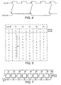
- Figure 7 is a circuit diagram of a divide-by-eight circuit, which has eight transistor stages S1 to S8, each of which is of the type labelled S1 to S4 in Figure 1, and a tri-state inverter stage labelled S9 similar to the stage S5 of Figure 1.
- Figures 8a to 8j represent the waveforms for the circuit of Figure 7.
- Figure 8a shows an input signal having a 50% duty cycle applied to the divide-by-eight circuit of Figure 7.
- Figure 8b illustrates the output waveform for the output signal CLK OUT at the output node of the tri-state inverter stage S9. As can be seen, this has a duty cycle of 50%.
- Figures 8c to 8j are the output signals from the other output nodes of the stages in the ring, labelled V2 to V9. The signals at these nodes each represent a divide-by-four version of the input signal, but not at a duty cycle of 50%.
- Figure 9 illustrates how a programmable dividing circuit may be constructed to divide by a selected even integer M.
- Figure 9 illustrates a programmable dividing circuit which can selectively divide by four or six.
- the circuit comprises six transistor stages S'1 to S'6 and a tri-state inverter stage S'7 connected in a ring.
- the transistor configuration of each of the stages S'1 to S'6 is not shown in Figure 9 but is the same as for Figure 1.
- the tri-state inverter stage S'7 can take the form illustrated in Figure 1 or any suitable alternative tri-state inverter circuit known in the art.
- a multiplexer 20 has one input connected to the output of the transistor stage S'6 and another input connected to the output of the fourth stage S'4.
- the output of the multiplexer 20 forms the input to the tri-state inverter stage S'7.
- the multiplexer 20 has a select input 22 which receives a select signal SEL which controls whether the output of the sixth transistor stage or the fourth transistor stage is supplied as the input to the tri-state inverter stage S'7. It will be appreciated that any suitable multiplexer could be used to selectively supply the output of the fourth or sixth stage as the input of the tri-state inverter stage S'7. It can thus be understood that the circuit can be programmed to divide by four or six depending on the state of the select signal SEL.
- the output of the fourth stage S'4 is supplied as the input to the tri-state inverter stage S'7 so that the ring operates as a divide-by-four ring as described above with reference to Figure 1. If the select signal cell goes high, the output of the sixth stage S'6 is supplied as the input to the tri-state inverter stage S'7 so that the ring operates as a divide-by-six ring. It is possible to change the dividing integer M "on the fly" by appropriately selecting the time at which the state of the select input is changed relative to the clock signal CLK IN.
- FIG 11 is a diagram of a basic phase-locked-loop circuit in which the dividing circuits described herein are particularly useful.
- the phase-locked-loop receives a reference clock input REF CLK IN and generates a PLL clock output PLL CLK OUT.
- An input divider 50 creates from the reference clock input REF CLK IN a reference input frequency for a phase detector 52.
- the phase detector 52 also receives as an input a feedback signal ⁇ generated in a manner described in the following. If the two inputs to the phase detector differ in phase, an error output e is generated and is supplied to a charge pump 54.
- a loop filter 56 shapes the output of the charge pump 54 and generates a correction signal for a voltage controlled oscillator 58.
- the output of the voltage controlled oscillator is passed through a feedback divider 60 to generate the second input ⁇ to the phase detector.
- the output of the voltage controlled oscillator is also passed through an output divider 62 to generate the clock output PLL CLK OUT.
- a dividing circuit in accordance with the present invention can usefully be used to implement any of the input divider 50, feedback divider 60 or output divider 62 to provide a phase-locked-loop satisfying required technology, frequency and power constraints.
Landscapes
- Manipulation Of Pulses (AREA)
Applications Claiming Priority (2)
| Application Number | Priority Date | Filing Date | Title |
|---|---|---|---|
| GBGB9727247.0A GB9727247D0 (en) | 1997-12-23 | 1997-12-23 | A dividing circuit for dividing by even numbers |
| GB9727247 | 1997-12-23 |
Publications (2)
| Publication Number | Publication Date |
|---|---|
| EP0926832A1 true EP0926832A1 (fr) | 1999-06-30 |
| EP0926832B1 EP0926832B1 (fr) | 2002-03-20 |
Family
ID=10824170
Family Applications (1)
| Application Number | Title | Priority Date | Filing Date |
|---|---|---|---|
| EP98310168A Expired - Lifetime EP0926832B1 (fr) | 1997-12-23 | 1998-12-11 | Circuit diviseur pour diviser par des nombres pairs |
Country Status (4)
| Country | Link |
|---|---|
| US (1) | US6097783A (fr) |
| EP (1) | EP0926832B1 (fr) |
| DE (1) | DE69804286T2 (fr) |
| GB (1) | GB9727247D0 (fr) |
Cited By (1)
| Publication number | Priority date | Publication date | Assignee | Title |
|---|---|---|---|---|
| WO2007004183A1 (fr) * | 2005-06-30 | 2007-01-11 | Nxp B.V. | Diviseur de frequence multiphase |
Families Citing this family (3)
| Publication number | Priority date | Publication date | Assignee | Title |
|---|---|---|---|---|
| US6518805B2 (en) * | 2000-10-04 | 2003-02-11 | Broadcom Corporation | Programmable divider with built-in programmable delay chain for high-speed/low power application |
| US6826250B2 (en) * | 2001-03-15 | 2004-11-30 | Seagate Technologies Llc | Clock divider with error detection and reset capabilities |
| US8344765B2 (en) * | 2009-07-16 | 2013-01-01 | Qualcomm, Incorporated | Frequency divider with a configurable dividing ratio |
Citations (3)
| Publication number | Priority date | Publication date | Assignee | Title |
|---|---|---|---|---|
| JPS6226920A (ja) * | 1985-07-29 | 1987-02-04 | Canon Inc | タイミング発生装置 |
| WO1990005413A1 (fr) * | 1988-10-31 | 1990-05-17 | Hughes Aircraft Company | Diviseur de frequence programmable numerique a haute vitesse |
| US4953187A (en) * | 1989-01-23 | 1990-08-28 | Motorola, Inc. | High speed prescaler |
Family Cites Families (6)
| Publication number | Priority date | Publication date | Assignee | Title |
|---|---|---|---|---|
| GB1373626A (en) * | 1970-11-27 | 1974-11-13 | Smiths Industries Ltd | Electrical dividing circuits |
| US4114049A (en) * | 1972-02-25 | 1978-09-12 | Tokyo Shibaura Electric Co., Ltd. | Counter provided with complementary field effect transistor inverters |
| JPS5696532A (en) * | 1979-12-29 | 1981-08-04 | Citizen Watch Co Ltd | Frequency divider |
| US5304938A (en) * | 1992-11-18 | 1994-04-19 | Gec Plessey Semiconductors, Inc. | Method and apparatus for providing a lower frequency signal with reference to a higher frequency signal |
| US5425074A (en) * | 1993-12-17 | 1995-06-13 | Intel Corporation | Fast programmable/resettable CMOS Johnson counters |
| US5854576A (en) * | 1997-04-21 | 1998-12-29 | Ati Technologies | Method and apparatus for a finely adjustable clock circuit |
-
1997
- 1997-12-23 GB GBGB9727247.0A patent/GB9727247D0/en not_active Ceased
-
1998
- 1998-12-11 EP EP98310168A patent/EP0926832B1/fr not_active Expired - Lifetime
- 1998-12-11 DE DE69804286T patent/DE69804286T2/de not_active Expired - Fee Related
- 1998-12-23 US US09/221,669 patent/US6097783A/en not_active Expired - Fee Related
Patent Citations (3)
| Publication number | Priority date | Publication date | Assignee | Title |
|---|---|---|---|---|
| JPS6226920A (ja) * | 1985-07-29 | 1987-02-04 | Canon Inc | タイミング発生装置 |
| WO1990005413A1 (fr) * | 1988-10-31 | 1990-05-17 | Hughes Aircraft Company | Diviseur de frequence programmable numerique a haute vitesse |
| US4953187A (en) * | 1989-01-23 | 1990-08-28 | Motorola, Inc. | High speed prescaler |
Non-Patent Citations (1)
| Title |
|---|
| PATENT ABSTRACTS OF JAPAN vol. 011, no. 204 (E - 520) 2 July 1987 (1987-07-02) * |
Cited By (1)
| Publication number | Priority date | Publication date | Assignee | Title |
|---|---|---|---|---|
| WO2007004183A1 (fr) * | 2005-06-30 | 2007-01-11 | Nxp B.V. | Diviseur de frequence multiphase |
Also Published As
| Publication number | Publication date |
|---|---|
| US6097783A (en) | 2000-08-01 |
| GB9727247D0 (en) | 1998-02-25 |
| DE69804286D1 (de) | 2002-04-25 |
| EP0926832B1 (fr) | 2002-03-20 |
| DE69804286T2 (de) | 2002-10-31 |
Similar Documents
| Publication | Publication Date | Title |
|---|---|---|
| US6914460B1 (en) | Counter-based clock doubler circuits and methods | |
| US4953187A (en) | High speed prescaler | |
| US7292079B2 (en) | DLL-based programmable clock generator using a threshold-trigger delay element circuit and a circular edge combiner | |
| US6566918B1 (en) | Divide-by-N clock divider circuit with minimal additional delay | |
| US6411669B1 (en) | Dual-modulus prescaler for RF synthesizer | |
| CA2159762C (fr) | Commande de rapport cyclique integree a un synthetiseur de frequence | |
| KR970006394B1 (ko) | 다상 클럭 발생 회로 | |
| US7196561B2 (en) | Programmable reset signal that is independent of supply voltage ramp rate | |
| US5059838A (en) | Signal delay circuit using charge pump circuit | |
| US10523211B2 (en) | Wide range glitchless switchable clock divider with modified 2/3 divider stages | |
| JP3601961B2 (ja) | デュアル・モジュラス・プリスケーラ | |
| US5221863A (en) | Phase-locked loop clock signal generator | |
| US7332945B2 (en) | Divider having dual modulus pre-scaler and an associated method | |
| US7388442B2 (en) | Digitally controlled oscillator for reduced power over process variations | |
| US6522711B2 (en) | Variable frequency divider circuit | |
| US6967512B2 (en) | Multiphase-clock processing circuit and clock multiplying circuit | |
| US4715052A (en) | Frequency divide by N circuit | |
| US6154077A (en) | Bistable flip-flop | |
| US6208179B1 (en) | Dividing circuit and transistor stage therefor | |
| US6133796A (en) | Programmable divider circuit with a tri-state inverter | |
| EP0926832B1 (fr) | Circuit diviseur pour diviser par des nombres pairs | |
| CN110214417B (zh) | 50%占空比正交输入正交输出(qiqo)3分频电路 | |
| CN114844486A (zh) | 可加载真单相时钟触发器 | |
| JPH0427729B2 (fr) | ||
| US6222401B1 (en) | Phase locked loop using gear shifting algorithm |
Legal Events
| Date | Code | Title | Description |
|---|---|---|---|
| PUAI | Public reference made under article 153(3) epc to a published international application that has entered the european phase |
Free format text: ORIGINAL CODE: 0009012 |
|
| AK | Designated contracting states |
Kind code of ref document: A1 Designated state(s): DE FR GB IT |
|
| AX | Request for extension of the european patent |
Free format text: AL;LT;LV;MK;RO;SI |
|
| 17P | Request for examination filed |
Effective date: 19991202 |
|
| AKX | Designation fees paid |
Free format text: DE FR GB IT |
|
| 17Q | First examination report despatched |
Effective date: 20001122 |
|
| GRAG | Despatch of communication of intention to grant |
Free format text: ORIGINAL CODE: EPIDOS AGRA |
|
| GRAG | Despatch of communication of intention to grant |
Free format text: ORIGINAL CODE: EPIDOS AGRA |
|
| GRAH | Despatch of communication of intention to grant a patent |
Free format text: ORIGINAL CODE: EPIDOS IGRA |
|
| GRAH | Despatch of communication of intention to grant a patent |
Free format text: ORIGINAL CODE: EPIDOS IGRA |
|
| REG | Reference to a national code |
Ref country code: GB Ref legal event code: IF02 |
|
| GRAA | (expected) grant |
Free format text: ORIGINAL CODE: 0009210 |
|
| AK | Designated contracting states |
Kind code of ref document: B1 Designated state(s): DE FR GB IT |
|
| PG25 | Lapsed in a contracting state [announced via postgrant information from national office to epo] |
Ref country code: IT Free format text: LAPSE BECAUSE OF FAILURE TO SUBMIT A TRANSLATION OF THE DESCRIPTION OR TO PAY THE FEE WITHIN THE PRESCRIBED TIME-LIMIT;WARNING: LAPSES OF ITALIAN PATENTS WITH EFFECTIVE DATE BEFORE 2007 MAY HAVE OCCURRED AT ANY TIME BEFORE 2007. THE CORRECT EFFECTIVE DATE MAY BE DIFFERENT FROM THE ONE RECORDED. Effective date: 20020320 |
|
| REF | Corresponds to: |
Ref document number: 69804286 Country of ref document: DE Date of ref document: 20020425 |
|
| ET | Fr: translation filed | ||
| ET | Fr: translation filed | ||
| PLBE | No opposition filed within time limit |
Free format text: ORIGINAL CODE: 0009261 |
|
| STAA | Information on the status of an ep patent application or granted ep patent |
Free format text: STATUS: NO OPPOSITION FILED WITHIN TIME LIMIT |
|
| 26N | No opposition filed |
Effective date: 20021223 |
|
| PGFP | Annual fee paid to national office [announced via postgrant information from national office to epo] |
Ref country code: GB Payment date: 20051207 Year of fee payment: 8 |
|
| PGFP | Annual fee paid to national office [announced via postgrant information from national office to epo] |
Ref country code: FR Payment date: 20051208 Year of fee payment: 8 |
|
| PGFP | Annual fee paid to national office [announced via postgrant information from national office to epo] |
Ref country code: DE Payment date: 20051209 Year of fee payment: 8 |
|
| PG25 | Lapsed in a contracting state [announced via postgrant information from national office to epo] |
Ref country code: DE Free format text: LAPSE BECAUSE OF NON-PAYMENT OF DUE FEES Effective date: 20070703 |
|
| GBPC | Gb: european patent ceased through non-payment of renewal fee |
Effective date: 20061211 |
|
| REG | Reference to a national code |
Ref country code: FR Ref legal event code: ST Effective date: 20070831 |
|
| PG25 | Lapsed in a contracting state [announced via postgrant information from national office to epo] |
Ref country code: GB Free format text: LAPSE BECAUSE OF NON-PAYMENT OF DUE FEES Effective date: 20061211 |
|
| PG25 | Lapsed in a contracting state [announced via postgrant information from national office to epo] |
Ref country code: FR Free format text: LAPSE BECAUSE OF NON-PAYMENT OF DUE FEES Effective date: 20070102 |