EP0926617B1 - A smart card reader - Google Patents
A smart card reader Download PDFInfo
- Publication number
- EP0926617B1 EP0926617B1 EP98124443A EP98124443A EP0926617B1 EP 0926617 B1 EP0926617 B1 EP 0926617B1 EP 98124443 A EP98124443 A EP 98124443A EP 98124443 A EP98124443 A EP 98124443A EP 0926617 B1 EP0926617 B1 EP 0926617B1
- Authority
- EP
- European Patent Office
- Prior art keywords
- contact elements
- cover
- smart
- base
- card reader
- Prior art date
- Legal status (The legal status is an assumption and is not a legal conclusion. Google has not performed a legal analysis and makes no representation as to the accuracy of the status listed.)
- Expired - Lifetime
Links
Images

Classifications
-
- G—PHYSICS
- G06—COMPUTING OR CALCULATING; COUNTING
- G06K—GRAPHICAL DATA READING; PRESENTATION OF DATA; RECORD CARRIERS; HANDLING RECORD CARRIERS
- G06K7/00—Methods or arrangements for sensing record carriers, e.g. for reading patterns
- G06K7/0013—Methods or arrangements for sensing record carriers, e.g. for reading patterns by galvanic contacts, e.g. card connectors for ISO-7816 compliant smart cards or memory cards, e.g. SD card readers
- G06K7/0034—Methods or arrangements for sensing record carriers, e.g. for reading patterns by galvanic contacts, e.g. card connectors for ISO-7816 compliant smart cards or memory cards, e.g. SD card readers the connector being capable of simultaneously receiving a plurality of cards in the same insertion slot
-
- G—PHYSICS
- G06—COMPUTING OR CALCULATING; COUNTING
- G06K—GRAPHICAL DATA READING; PRESENTATION OF DATA; RECORD CARRIERS; HANDLING RECORD CARRIERS
- G06K7/00—Methods or arrangements for sensing record carriers, e.g. for reading patterns
- G06K7/0013—Methods or arrangements for sensing record carriers, e.g. for reading patterns by galvanic contacts, e.g. card connectors for ISO-7816 compliant smart cards or memory cards, e.g. SD card readers
- G06K7/0021—Methods or arrangements for sensing record carriers, e.g. for reading patterns by galvanic contacts, e.g. card connectors for ISO-7816 compliant smart cards or memory cards, e.g. SD card readers for reading/sensing record carriers having surface contacts
Definitions
- the invention relates to a smart-card reader and in particular to a smart-card reader which is useful for different applications.
- a smart card or chip card reader i.e. a contacting apparatus comprising a contact element support or frame within which contact elements are fixedly mounted.
- a cover can be mounted on said contact element support, so as to form together with said frame an insert slot into which a smart card can be inserted into a card reading position.
- the cover is not required if a surface is provided by the apparatus in which the smart-card reader is used, a surface which assumes the function of the cover.
- the contact elements of the smart-card reader which are also sometimes called reading contact elements, engage or contact so-called card contacts which are formed on at least one surface of said smart card.
- Smart card readers can be installed into certain apparatuses, for instance a television set so as to be used together with a smart card for the control of the operation of such an apparatus.
- GB-A-2298743 discloses a card reader for accepting and providing electrical connections to two EC cards simultaneously.
- the card reader comprises first and second wall members, each carrying a plurality of metallic leaf springs which will act as electrical connectors.
- the connectors are arranged and shapes such that they project into the card receiving slot.
- manually operable means in the form of a rotatable rod are provided to bias a single card towards the inner surface of one of the wall members.
- space in the apparatus in which the smart-card reader is used is saved, and the cost of installing readers is reduced.
- a smart-card reader which can be readily soldered into a printed circuit board of a customer to be used in an apparatus in which the smart card reader is to be based.
- the connecting means are provided for the termination ends or portions of the contact elements either in the cover or in the base.
- the termination ends of the contact elements in the cover are extended by said connecting means to a level of the termination ends of the contact elements in the base.
- an end position switch is located in the cover or the base, preferably in the cover.
- Said end position switch comprises two contact elements fixedly mounted in the base or cover.
- a smart-card reader which comprises a base with contact elements having termination ends forming soldering contacts adapted to be soldered into a printed circuit board and projecting away from the bottom surface of said base.
- the bottom surface is opposite to an upper surface of the base adjacent to which the contacting ends or portions of the contact elements are located.
- the smart-card reader further comprises a cover in substance similar to said base and also carrying contact elements with termination ends forming soldering contacts and projecting away from an upper surface of the cover which is opposite to a bottom surface of the cover adjacent to which the contacting ends or portions of the contact elements are located.
- the cover is placed on the base such that the bottom surface of the cover and the upper surface of the base (close to which the contacting ends of the contact elements are located) face towards each other thus forming said card insert slot.
- Means are provided to connect the termination ends of all the contact elements including the contact elements forming the end position switch such that the entire smart-card reader can be readily connected with a customer circuit board.
- Said connecting means electrically connect all contact element termination ends of said first or said second group, such that all terminations of said contact elements are one side of the smart-card reader.
- any kind of galvanic connection can be provided between the contact elements in the cover and/or base, so that they can be readily connected to the customer circuit board.
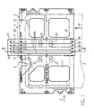
- FIGs 1, 2, 3 and 4 show the smart-card reader 1 in accordance with the invention.
- a smart card 2 is shown schematically as being inserted into said chip-card reader 1 in the direction of arrow B ( Figure 1).
- Figure 2 shows that the smart-card reader 1 comprises a first or upper portion 3 and a second or lower portion 4.
- the upper portion 3 will be called below a cover 3 and the lower portion 4 will be called below a base 4.
- the cover 3 is identical or very similar to the base 4 and is just turned by 180° and placed on top of the base 4.
- Figure 2 and 5 show a first group of two times four, i.e. eight reading contact elements 5, 55 is fixedly mounted in the cover 3.
- the contact elements 55 are behind (left in Figure 4) the contact elements 5.
- the base 4 there are also eight contact elements 6, 66 fixedly mounted forming a second group of contact elements.
- the contact elements of each group are arranged in two sub groups of each four contact elements.
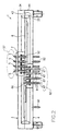
- Figure 4 shows each of the identical contact elements 5, 55; 6, 66 as comprising a termination end or portion 56, 57; 67, 68 which is angled by about 90° with respect to a substantially longitudinal portion 84.
- the longitudinal portion 84 forms a contacting portion or end in the form of a cusp 82.
- the cusp 82 continues and ends in an abutment portion 88 which can abut at an abutment surface 86, 87 formed by said cover and base, respectively.
- the contact element forms detent means in the form of a snap arm 85 stamped out of the material of the contact element.
- Said snap arm 84 co-operates with respective detent means of the base and cover, respectively, for instance with a snap in surface 95 shown in Figure 4 for the contact element 5.
- first group of contact elements 5 55 termination ends 56, 57 are bent upwardly ( Figure 2 and 4).
- the termination ends 67, 68 are bent downwardly ( Figure 2 and 4).
- a connecting means 7 in the form of a printed circuit board having a front end and a rear end extends from a front end of the cover 3 to a rear end of the cover 3 and beyond the rear end of the cover 3 forming an overhanging portion 79 ( Figure 3).
- the termination ends 56, 57 of the contact elements of the first group extend upwardly, while the termination ends 67, 68 of the contact elements of the second group extend downwardly.
- the upwardly extending termination ends 56, 57 of the contact elements are connected to conductive paths 105 of the printed circuit board 7. Said conductive paths 105 lead to the overhang portion 79 which extends beyond said cover portion rear end.
- pins 71 are connected to said conductive paths 105 and extend downwardly to the level of the termination ends 67, 68 of the contact elements 6, 66 of the base 4.
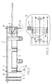
- Figure 5 discloses a top plan view of the customer circuit board 10 without a smart card reader yet being mounted thereon. Pins 71 in the overhanging portion 79 of the circuit board 7 are adapted to be inserted into holes C1 through C8 of the customer circuit board 10. This group of holes C1 through C8 is referred to by reference numeral 51 in Figure 5. Thus, the first group of contact elements 5, 55 are connected to the circuit board 10.
- the termination ends of the contact elements 6, 66 mounted in the base 4 extend downwardly like the soldering pins 71 in Figure 1 and 2 and are adapted to extend through the holes of a group of holes 61.
- Group 61 forms sub groups 62' and 63' as shown in Figure 5 corresponding to the sub groups 62, 63 of the contact elements 6, 66.
- respective mounting pins 106 of the base 4 can be inserted as is shown in Figure 5 to fixedly mount the base 4 on board 10.
- the cover 3 has an upper surface 31 and a lower surface 32 beyond which the cusps 82 of the contact elements 5, 55 extend.
- the base 4 has an upper surface 41 and a lower surface 42.
- the cusps 82 of the contact elements 6, 66 in the base 4 extend beyond said upper surface 41.
- the lower surface 32 and the upper surface 41 form a card insert slot 8.
- Both the cover and the base have U-shaped side walls 34 and 44, respectively forming U-shaped surfaces 33, 43 which face towards each other and are preferably adhesively bonded together.
- Figure 1 shows an end position switch having two contact elements located in the base 4.
- Both the cover and base have cut out portions 111 as is shown in Figure 1.
- reference numerals 21 and 22 refer to each one smart card contact out of two groups of card contacts of the smart card 2. These contacts 21, 22 can actually not be seen in the situation of Figure 1.
- a smart card has typically its card contacts (like 21 or. 22) on only one surface. If such a smart card is assumed to have been inserted in Figure 1, then e.g. the card contacts 21 face upwardly. if the card is turned by 180° then the card contacts would face downwardly, i.e. the card contacts would be there referred to by 22.
- the card contacts 22 are those which would be for instance contacted by the contact elements located in the base 4 if the smart card 2 is inserted with the card contacts 22 facing (see Figure 2) downwardly.
Landscapes
- Engineering & Computer Science (AREA)
- Artificial Intelligence (AREA)
- Computer Vision & Pattern Recognition (AREA)
- Physics & Mathematics (AREA)
- General Physics & Mathematics (AREA)
- Theoretical Computer Science (AREA)
- Coupling Device And Connection With Printed Circuit (AREA)
Applications Claiming Priority (2)
| Application Number | Priority Date | Filing Date | Title |
|---|---|---|---|
| DE19757626A DE19757626B4 (de) | 1997-12-23 | 1997-12-23 | Chipkartenleser für unterschiedliche Verwendungszwecke |
| DE19757626 | 1997-12-23 |
Publications (3)
| Publication Number | Publication Date |
|---|---|
| EP0926617A2 EP0926617A2 (en) | 1999-06-30 |
| EP0926617A3 EP0926617A3 (en) | 2000-06-21 |
| EP0926617B1 true EP0926617B1 (en) | 2002-08-21 |
Family
ID=7853239
Family Applications (1)
| Application Number | Title | Priority Date | Filing Date |
|---|---|---|---|
| EP98124443A Expired - Lifetime EP0926617B1 (en) | 1997-12-23 | 1998-12-22 | A smart card reader |
Country Status (4)
| Country | Link |
|---|---|
| US (2) | US6234391B1 (enExample) |
| EP (1) | EP0926617B1 (enExample) |
| JP (1) | JPH11250194A (enExample) |
| DE (2) | DE19757626B4 (enExample) |
Families Citing this family (10)
| Publication number | Priority date | Publication date | Assignee | Title |
|---|---|---|---|---|
| FR2801431B1 (fr) * | 1999-11-18 | 2002-03-22 | Gemplus Card Int | Connecteur pour carte a puce independant du sens d'insertion de la carte |
| US6659348B2 (en) * | 2000-01-24 | 2003-12-09 | Sankyo Seiki Mfg. Co., Ltd. | Manual IC card reader and manual card reader |
| US6676016B1 (en) * | 2000-05-04 | 2004-01-13 | Ncr Corporation | Retail terminal configured as consumer gateway to electronic billing application |
| JP4576669B2 (ja) * | 2000-06-06 | 2010-11-10 | 株式会社デンソー | カードリーダライタ |
| US7344074B2 (en) * | 2002-04-08 | 2008-03-18 | Nokia Corporation | Mobile terminal featuring smart card interrupt |
| TWM250251U (en) * | 2002-07-02 | 2004-11-11 | Carry Computer Eng Co Ltd | Improved structure for signal adapter of memory card |
| DE10256716A1 (de) * | 2002-12-04 | 2004-06-24 | Siemens Ag | Chipkartenaufnahme |
| DE10321242B4 (de) * | 2003-05-12 | 2008-04-10 | Siemens Ag | Kartenaufnahmevorrichtung |
| US9076050B2 (en) | 2013-03-12 | 2015-07-07 | Echostar Technologies L.L.C. | Enhanced smartcard reader with multi-level reading contacts |
| US10265137B2 (en) | 2014-07-09 | 2019-04-23 | Neil Glossop | Systems, methods, and devices for assisting or performing guided interventional procedures using custom templates |
Family Cites Families (20)
| Publication number | Priority date | Publication date | Assignee | Title |
|---|---|---|---|---|
| JPS6111284U (ja) | 1984-06-26 | 1986-01-23 | 沖電線株式会社 | 基板接続コネクタ |
| JPH0766425B2 (ja) * | 1986-05-02 | 1995-07-19 | 日本電気株式会社 | Icカ−ドのリ−ダ・ライタ |
| JPH0823878B2 (ja) * | 1988-04-21 | 1996-03-06 | 沖電気工業株式会社 | カード書込み・読出し装置 |
| JPH0286940A (ja) | 1988-09-24 | 1990-03-27 | Mitsubishi Electric Corp | 内燃機関の制御装置 |
| JPH04168094A (ja) * | 1990-10-31 | 1992-06-16 | Mitsubishi Electric Corp | 携帯形半導体記憶装置 |
| DE4212150A1 (de) * | 1991-11-12 | 1993-05-13 | Amphenol Tuchel Elect | Chipkartenlesegeraet mit einem endlagenschalter |
| US5810620A (en) * | 1992-10-29 | 1998-09-22 | Olympus Optical Co., Ltd. | Electric connector provided with a shielding part for electrical contacts at the distal end of the plug |
| US5726432A (en) * | 1993-05-14 | 1998-03-10 | Amphenol-Tuchel Electronics Gmbh | Contacting system or reader for chip cards |
| DE9418193U1 (de) * | 1994-11-12 | 1995-01-26 | Fischer Computersysteme GmbH + Co. KG, 78052 Villingen-Schwenningen | Kontaktiereinheit für ein Chipkarten-Schreib-/Lesegerät |
| DE19506801C2 (de) * | 1995-02-27 | 1998-04-16 | Siemens Nixdorf Inf Syst | Anordnung zur EMV-gerechten Herausführung eines auf einer Leiterplatte angeordneten elektrischen Anschlusses aus einem abschirmenden Gehäuse |
| GB2298743B (en) | 1995-03-10 | 1998-10-14 | Kenven Developments Limited | A connector for making surface electrical connections to IC cards |
| DE19521728B4 (de) * | 1995-06-14 | 2004-03-11 | Amphenol-Tuchel Electronics Gmbh | Chipkartenleser mit einem Schiebeschalter |
| EP0883855B1 (en) * | 1996-02-29 | 1999-12-08 | The Whitaker Corporation | Apparatus for the electrical connection of a chip card to a printed circuit board |
| DE19624079C1 (de) * | 1996-06-17 | 1998-01-29 | Bosch Gmbh Robert | Kartenleser für Chipkarten |
| EP0845750A3 (de) * | 1996-11-29 | 2000-11-29 | Tyco Electronics Logistics AG | Doppelstöckiger Stecker für zwei Chipkarten |
| US6015311A (en) * | 1996-12-17 | 2000-01-18 | The Whitaker Corporation | Contact configuration for smart card reader |
| US6112994A (en) * | 1997-02-27 | 2000-09-05 | The Whitaker Corporation | Card reader connector with attachable cover |
| US6149466A (en) * | 1997-05-13 | 2000-11-21 | Itt Manufacturing Enterprises, Inc. | Compact smart card electrical connector |
| US6049463A (en) * | 1997-07-25 | 2000-04-11 | Motorola, Inc. | Microelectronic assembly including an antenna element embedded within a polymeric card, and method for forming same |
| US6024593A (en) * | 1997-10-14 | 2000-02-15 | The Whitaker Corporation | Electronic module connector having a locking cover |
-
1997
- 1997-12-23 DE DE19757626A patent/DE19757626B4/de not_active Expired - Fee Related
-
1998
- 1998-12-22 DE DE69807312T patent/DE69807312T2/de not_active Expired - Lifetime
- 1998-12-22 US US09/217,618 patent/US6234391B1/en not_active Expired - Fee Related
- 1998-12-22 EP EP98124443A patent/EP0926617B1/en not_active Expired - Lifetime
- 1998-12-24 JP JP10368164A patent/JPH11250194A/ja active Pending
-
2000
- 2000-11-30 US US09/726,034 patent/US6398111B2/en not_active Expired - Fee Related
Also Published As
| Publication number | Publication date |
|---|---|
| JPH11250194A (ja) | 1999-09-17 |
| US6234391B1 (en) | 2001-05-22 |
| EP0926617A2 (en) | 1999-06-30 |
| DE69807312T2 (de) | 2003-04-17 |
| DE19757626A1 (de) | 1999-06-24 |
| DE69807312D1 (de) | 2002-09-26 |
| US20010002034A1 (en) | 2001-05-31 |
| US6398111B2 (en) | 2002-06-04 |
| EP0926617A3 (en) | 2000-06-21 |
| DE19757626B4 (de) | 2005-08-25 |
Similar Documents
| Publication | Publication Date | Title |
|---|---|---|
| US5563770A (en) | IC card with board positioning means | |
| CA2179044C (en) | Ic card with board positioning means | |
| EP0926769B1 (en) | Very thin electrical connector for the connection of a smart card | |
| KR100585547B1 (ko) | 카드 커넥터 | |
| KR19990067235A (ko) | 스마트 카드 및 스마트 카드 커넥터 | |
| US5975959A (en) | Smart card connector module | |
| JP2000315534A (ja) | スマートカードコネクタ | |
| JPH06309517A (ja) | 遮蔽メモリカードホルダ | |
| US6835100B1 (en) | Multi-in-one connector structure | |
| US6091605A (en) | Memory card connector and cover apparatus and method | |
| EP0926617B1 (en) | A smart card reader | |
| US6551131B1 (en) | Stacked electrical card connector assembly | |
| EP1059600B1 (en) | Portable smart card reader assembly | |
| US5924881A (en) | Electrical connector for IC card | |
| US6050857A (en) | SIM connector and related contact | |
| US7051931B2 (en) | Chip card reader | |
| EP0921490B1 (en) | Electrical connector device for co-operating with a removable electronic medium | |
| KR100552322B1 (ko) | 전기 커넥터 | |
| US4629267A (en) | Circuit terminating device | |
| US20030114043A1 (en) | Stacked electrical card connector assembly | |
| US20050118877A1 (en) | Memory card connector | |
| US20010031577A1 (en) | Connection-retaining unit | |
| CA2174130C (en) | Ic card with board positioning means | |
| EP1427062B1 (en) | Electric connector | |
| US6478615B1 (en) | Stacked electrical card connector assembly |
Legal Events
| Date | Code | Title | Description |
|---|---|---|---|
| PUAI | Public reference made under article 153(3) epc to a published international application that has entered the european phase |
Free format text: ORIGINAL CODE: 0009012 |
|
| AK | Designated contracting states |
Kind code of ref document: A2 Designated state(s): BE DE FR GB IT NL SE |
|
| AX | Request for extension of the european patent |
Free format text: AL;LT;LV;MK;RO;SI |
|
| PUAL | Search report despatched |
Free format text: ORIGINAL CODE: 0009013 |
|
| AK | Designated contracting states |
Kind code of ref document: A3 Designated state(s): AT BE CH CY DE DK ES FI FR GB GR IE IT LI LU MC NL PT SE |
|
| AX | Request for extension of the european patent |
Free format text: AL;LT;LV;MK;RO;SI |
|
| 17P | Request for examination filed |
Effective date: 20000721 |
|
| AKX | Designation fees paid |
Free format text: BE DE FR GB IT NL SE |
|
| 17Q | First examination report despatched |
Effective date: 20010117 |
|
| GRAG | Despatch of communication of intention to grant |
Free format text: ORIGINAL CODE: EPIDOS AGRA |
|
| GRAG | Despatch of communication of intention to grant |
Free format text: ORIGINAL CODE: EPIDOS AGRA |
|
| GRAH | Despatch of communication of intention to grant a patent |
Free format text: ORIGINAL CODE: EPIDOS IGRA |
|
| GRAH | Despatch of communication of intention to grant a patent |
Free format text: ORIGINAL CODE: EPIDOS IGRA |
|
| GRAH | Despatch of communication of intention to grant a patent |
Free format text: ORIGINAL CODE: EPIDOS IGRA |
|
| GRAA | (expected) grant |
Free format text: ORIGINAL CODE: 0009210 |
|
| AK | Designated contracting states |
Kind code of ref document: B1 Designated state(s): BE DE FR GB IT NL SE |
|
| REG | Reference to a national code |
Ref country code: GB Ref legal event code: FG4D |
|
| REF | Corresponds to: |
Ref document number: 69807312 Country of ref document: DE Date of ref document: 20020926 |
|
| ET | Fr: translation filed | ||
| PLBE | No opposition filed within time limit |
Free format text: ORIGINAL CODE: 0009261 |
|
| STAA | Information on the status of an ep patent application or granted ep patent |
Free format text: STATUS: NO OPPOSITION FILED WITHIN TIME LIMIT |
|
| 26N | No opposition filed |
Effective date: 20030522 |
|
| PGFP | Annual fee paid to national office [announced via postgrant information from national office to epo] |
Ref country code: NL Payment date: 20031110 Year of fee payment: 6 |
|
| PGFP | Annual fee paid to national office [announced via postgrant information from national office to epo] |
Ref country code: SE Payment date: 20031202 Year of fee payment: 6 |
|
| PGFP | Annual fee paid to national office [announced via postgrant information from national office to epo] |
Ref country code: BE Payment date: 20040114 Year of fee payment: 6 |
|
| PG25 | Lapsed in a contracting state [announced via postgrant information from national office to epo] |
Ref country code: SE Free format text: LAPSE BECAUSE OF NON-PAYMENT OF DUE FEES Effective date: 20041223 |
|
| PG25 | Lapsed in a contracting state [announced via postgrant information from national office to epo] |
Ref country code: BE Free format text: LAPSE BECAUSE OF NON-PAYMENT OF DUE FEES Effective date: 20041231 |
|
| BERE | Be: lapsed |
Owner name: *AMPHENOL-TUCHEL ELECTRONICS G.M.B.H. Effective date: 20041231 |
|
| PG25 | Lapsed in a contracting state [announced via postgrant information from national office to epo] |
Ref country code: NL Free format text: LAPSE BECAUSE OF NON-PAYMENT OF DUE FEES Effective date: 20050701 |
|
| EUG | Se: european patent has lapsed | ||
| NLV4 | Nl: lapsed or anulled due to non-payment of the annual fee |
Effective date: 20050701 |
|
| BERE | Be: lapsed |
Owner name: *AMPHENOL-TUCHEL ELECTRONICS G.M.B.H. Effective date: 20041231 |
|
| PGFP | Annual fee paid to national office [announced via postgrant information from national office to epo] |
Ref country code: IT Payment date: 20071218 Year of fee payment: 10 |
|
| PGFP | Annual fee paid to national office [announced via postgrant information from national office to epo] |
Ref country code: FR Payment date: 20081205 Year of fee payment: 11 |
|
| PGFP | Annual fee paid to national office [announced via postgrant information from national office to epo] |
Ref country code: GB Payment date: 20081110 Year of fee payment: 11 |
|
| GBPC | Gb: european patent ceased through non-payment of renewal fee |
Effective date: 20091222 |
|
| REG | Reference to a national code |
Ref country code: FR Ref legal event code: ST Effective date: 20100831 |
|
| PG25 | Lapsed in a contracting state [announced via postgrant information from national office to epo] |
Ref country code: FR Free format text: LAPSE BECAUSE OF NON-PAYMENT OF DUE FEES Effective date: 20091231 |
|
| PG25 | Lapsed in a contracting state [announced via postgrant information from national office to epo] |
Ref country code: GB Free format text: LAPSE BECAUSE OF NON-PAYMENT OF DUE FEES Effective date: 20091222 |
|
| PG25 | Lapsed in a contracting state [announced via postgrant information from national office to epo] |
Ref country code: IT Free format text: LAPSE BECAUSE OF NON-PAYMENT OF DUE FEES Effective date: 20081222 |
|
| PGFP | Annual fee paid to national office [announced via postgrant information from national office to epo] |
Ref country code: DE Payment date: 20151217 Year of fee payment: 18 |
|
| REG | Reference to a national code |
Ref country code: DE Ref legal event code: R119 Ref document number: 69807312 Country of ref document: DE |
|
| PG25 | Lapsed in a contracting state [announced via postgrant information from national office to epo] |
Ref country code: DE Free format text: LAPSE BECAUSE OF NON-PAYMENT OF DUE FEES Effective date: 20170701 |