EP0922304B1 - Sensorelement - Google Patents
Sensorelement Download PDFInfo
- Publication number
- EP0922304B1 EP0922304B1 EP96939013A EP96939013A EP0922304B1 EP 0922304 B1 EP0922304 B1 EP 0922304B1 EP 96939013 A EP96939013 A EP 96939013A EP 96939013 A EP96939013 A EP 96939013A EP 0922304 B1 EP0922304 B1 EP 0922304B1
- Authority
- EP
- European Patent Office
- Prior art keywords
- floating gate
- field effect
- effect transistor
- sensor
- sensor device
- Prior art date
- Legal status (The legal status is an assumption and is not a legal conclusion. Google has not performed a legal analysis and makes no representation as to the accuracy of the status listed.)
- Expired - Lifetime
Links
Images

Classifications
-
- G—PHYSICS
- G11—INFORMATION STORAGE
- G11C—STATIC STORES
- G11C27/00—Electric analogue stores, e.g. for storing instantaneous values
- G11C27/005—Electric analogue stores, e.g. for storing instantaneous values with non-volatile charge storage, e.g. on floating gate or MNOS
-
- H—ELECTRICITY
- H10—SEMICONDUCTOR DEVICES; ELECTRIC SOLID-STATE DEVICES NOT OTHERWISE PROVIDED FOR
- H10F—INORGANIC SEMICONDUCTOR DEVICES SENSITIVE TO INFRARED RADIATION, LIGHT, ELECTROMAGNETIC RADIATION OF SHORTER WAVELENGTH OR CORPUSCULAR RADIATION
- H10F30/00—Individual radiation-sensitive semiconductor devices in which radiation controls the flow of current through the devices, e.g. photodetectors
- H10F30/20—Individual radiation-sensitive semiconductor devices in which radiation controls the flow of current through the devices, e.g. photodetectors the devices having potential barriers, e.g. phototransistors
- H10F30/21—Individual radiation-sensitive semiconductor devices in which radiation controls the flow of current through the devices, e.g. photodetectors the devices having potential barriers, e.g. phototransistors the devices being sensitive to infrared, visible or ultraviolet radiation
- H10F30/28—Individual radiation-sensitive semiconductor devices in which radiation controls the flow of current through the devices, e.g. photodetectors the devices having potential barriers, e.g. phototransistors the devices being sensitive to infrared, visible or ultraviolet radiation the devices being characterised by field-effect operation, e.g. junction field-effect phototransistors
- H10F30/2823—Individual radiation-sensitive semiconductor devices in which radiation controls the flow of current through the devices, e.g. photodetectors the devices having potential barriers, e.g. phototransistors the devices being sensitive to infrared, visible or ultraviolet radiation the devices being characterised by field-effect operation, e.g. junction field-effect phototransistors the devices being conductor-insulator-semiconductor devices, e.g. diodes or charge-coupled devices [CCD]
Definitions
- the present invention relates to a monolithically integrated Sensor element, one versus one sensitive field effect transistor to be detected physical quantity and has a non-volatile memory.
- a sensor element and a non-volatile one Memory through two separate components on one chip realize.
- a MOS transistor act as a sensor, and a second MOS transistor can act as non-volatile memory.
- CMOS transistors complementary metal-oxide-semiconductors
- EEPROMs are common because of their simple programming used as non-volatile digital storage.
- a analog storage of information in a single EEPROM cell can increase the storage density and the circuit techniques simplify for analog signal processing, if long-term storage is necessary.
- the actual sensor and the non-volatile memory are realized by two transistors, one large chip area required to implement a sensor element. Furthermore, due to manufacturing-related local parameter fluctuations Adjustment problems between the two Transistors, which form a sensor element, causing the Output signal is changed. There is also a signal processing unit necessary that the sensor signal and the Memory content processed.
- US-A-4,788,581 relates to a MOS dosimeter for one dose to measure within a radiation field.
- the dosimeter comprises a semiconductor substrate, an insulation layer the semiconductor substrate, which is resistant to radiation and which are provided with a floating gate is. There is also a metal contact with a semiconductor substrate connected.
- the floating gate is used to create a Accumulate charge, the accumulated charge of dosing corresponds to the radiation. The accumulation of cargo can be reset to use the dosimeter again become.
- JP-A-07115182 relates to a photoelectric converter with a memory function, in which in a silicon substrate a layer is provided in which a source and a drain layer is diffused.
- a floating gate is placed on a tunnel oxide film and further is a Control gate, which consists of polychrystalline silicon, deposited on the floating gate, with between an oxide film is arranged on these two gates.
- a photoelectric Is through the photoconductive layer and a converter transparent electrode formed.
- the object of the present invention is a space-saving sensor element with associated non-volatile To create storage, in which there is also no production-related caused local parameter fluctuations Adaptation problems exist between the sensor and memory cell.
- the present invention provides a sensor element in the Form of a physical versus a physical Size sensitive field effect transistor, whose gate electrode is designed as a floating gate.
- the gate electrode of the transistor is designed as a floating gate, can the same for both operating point setting of the transistor as well as storing a charge that one through corresponds to the physical quantity detected by the field effect transistor, be used.
- This is the field effect transistor with a comparator and a programming unit for the EEPROM, which is formed by the floating gate, is connected.
- non-volatile memory can be set the working point of the one to be recorded physical size sensitive field effect transistor, for storing coefficients for further signal processing or to store the detected signal be used yourself.
- the present invention is compared to one sensitive physical field to be detected physical field effect transistor a photosensitive transistor that has an optical Sensor with an integrated, programmable represents non-volatile EEPROM memory.
- the invention Sensor element can be in a standard single poly CMOS / EEPROM technology be realized. Furthermore, the invention Sensor element also in double poly CMOS / EEPROM technology be realized, whereby the Space requirement of the component can be further reduced.
- the sensor element according to the invention can realized using other technologies as long as the sensor is connected to a gate connector in its Working point can be adjusted.
- the sensitive to a physical quantity to be recorded Field effect transistor of the sensor element according to the invention be a CMOS pressure sensor or acceleration sensor, whose gate electrode can be moved locally. Will the Applying pressure or acceleration to the transistor, can the pressure or the acceleration by the local displacement of the gate electrode can be registered. If the pressure sensor or the acceleration sensor Executed gate electrode as a floating gate, can Integrate non-volatile memory in the sensor.
- the present invention eliminates the separation of the sensor and the memory chip is canceled.
- the sensor contains a floating gate that charges are stored non-volatilely can.
- the charges stored on the floating gate affect the operating point of the sensor. So this can stored non-volatile as an analog or digital value become. Consequently, one obtains with the present invention a sensor element that has an analog non-volatile memory in the sensor itself, which is used to set the working point, for example for offset correction, or can also be used for signal processing.
- the realization of the sensor and the memory in one Component saves a lot of chip area compared to the separate implementation according to the prior art, because practically two components are combined in one. Additional Manufacturing costs are not incurred because the same manufacturing process can be used. Furthermore, by caused local parameter fluctuations caused by production Deviations between sensor and memory cell eliminated, because the sensor and the memory cell in one component are integrated. Furthermore, there is no processing unit necessary that the sensor signal with the stored Value processed.
- the processing can in the invention Sensor element itself happen. The processing can for example by using the transistor characteristics in the different working areas of the transistor be performed.
- the non-volatile memory of the sensor can also do this be used to save the recorded sensor signal.
- a control loop there is so much charge transported to the floating gate that the output signal of the sensor reaches a defined value.
- the sensor signal is then as a charge change that is on the Floating gate is present, stored in the sensor.
- a photo field effect transistor 10 is formed in a substrate 12.
- the photo field effect transistor is a p-channel MOS transistor, the p + -doped source 14 and the p + -doped drain 16 of which are located in a floating n-well 18.
- a floating gate 20 that charges non-volatile can save.
- the floating gate 20 is designed such that a portion of the same over n-doped regions in the p-substrate 12 is arranged.
- a first n-doped Area 22 serves as an injection area, while a second n-doped region 24 serves as a control region.
- the floating gate 20 and the injection area 22 are opposite one another arranged such that between them a tunnel region 26 is formed.
- the threshold voltage V th shows an almost logarithmic dependence on the incident light intensity.
- the threshold voltage V th is also dependent on any charges that may be present on the floating gate.
- the threshold voltage V th can be defined, for example, as the gate voltage which causes a drain current of 10 ⁇ A at a drain-source voltage of 2 volts.
- Fig. 2 are optical characteristics of that shown in Fig. 1 Sensor elements in different preprogrammed Threshold voltages of the sensor transistor shown. These threshold voltages can be programmed by Electrons by applying a high voltage between them Control area 24 and the injection area 22 to the floating gate 20 moved or removed from the same. This happens through a tunnel effect between the injection area 22 and the section of the Floating gates 20.
- Fig. 2 the optical characteristics of the sensor are shown logarithmically for voltages V tho from 0.75 volts to 1.35 volts, V tho representing the threshold voltage V tho without light irradiation.
- V tho representing the threshold voltage V tho without light irradiation.
- the programmed threshold voltages do not change the logarithmic dependence of the characteristic curve of the sensor on the incident light intensity.
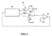
- the dashed mark 30 shows the circuit symbol of the photo field effect transistor with integrated EEPROM memory, which represents the sensor element according to the preferred exemplary embodiment of the invention.
- This sensor element is subjected to light irradiation 32.
- a supply voltage vdd is present at the source electrode of the transistor.
- the drain electrode of the transistor is connected to ground via a resistor R.
- the drain electrode is also connected to a first input of a comparator 34.
- the second input of the comparator is connected to a voltage source which applies a reference voltage V ref to the same.
- the output of the comparator is with a programming unit 36 for the EEPROM of the photo field effect transistor.
- the programming unit 36 is connected to the control area 24 and the injection area 22.
- the reference voltage V ref corresponds to the output voltage V i when there is no light radiation 32. If light is applied to the transistor 32, the threshold voltage of the transistor shifts, which results in a change in the output voltage V i . This is detected by the comparator 34, whereupon the programming unit 36 applies charges to the floating gate until the output voltage V i reaches the reference voltage V ref . If this is the case, the threshold voltage of the PMOS transistor changed by the light radiation 32 is compensated for by the charges on the floating gate, which bring about a shift in the threshold voltage. A voltage corresponding to the light output is thus stored as a threshold voltage change on the floating gate in the sensor.
- the present invention thus provides a monolithically integrated Sensor element in which manufacturing-related parameter fluctuations or adaptations to changing environmental conditions by an integrated in the sensor element non-volatile memory can be compensated.
- the Compensation information is placed on the floating gate saved.
- the inventive are also suitable Store well as analog memory, since they are the same as the analog one Signal of the sensor can process directly or one too Store the programming analog operating point voltage permanently can.
- the component according to the invention contains a sensor element and a non-volatile one at the same time Storage.
- the sensor element according to the present invention can be found in numerous applications, for example in the field of neural networks with non-volatile mass storage or in the field of educational cameras, the image patterns only can be learned by "viewing".
- the Non-volatile storage option also enables an offset and sensitivity correction of the sensor, so that a fixed pattern noise in large photosensor arrays can be eliminated.
Landscapes
- Semiconductor Memories (AREA)
Description
- Fig. 1
- schematisch den Aufbau eines bevorzugten Ausführungsbeispiels eines erfindungsgemäßen Sensorelements;
- Fig. 2
- eine Darstellung der optischen Kennlinien des in Fig. 1 dargestellten Sensorelements bei verschiedenen vorprogrammierten Schwellenspannungen; und
- Fig. 3
- eine schematische Darstellung einer Regelschleife zur Abspeicherung des Sensorsignals auf dem Sensorspeicher.
Claims (7)
- Sensorvorrichtung, mit
einem Sensorelement (30) in der Form eines gegenüber einer zu erfassenden physikalischen Größe empfindlichen Feldeffekttransistors (10), dessen Gate-Elektrode (20) als Floating-Gate ausgebildet ist;
dadurch gekennzeichnet, daß eine Änderung der Schwellenspannung (Vtho) des Feldeffekttransistors (10) in Äbhängigkeit von der erfaßten physikalischen Größe mittels einer Programmiereinheit (36) durch Zufuhr oder Entfernung von Ladungen auf das Floating-Gate kompensiert wird, wodurch die der physikalischen Größe entsprechende Schwellenspannungsänderung in Form dieser Ladungen auf dem Floating-Gate gespeichert wird. - Sensorvorrichtung gemäß Anspruch 1, dadurch gekennzeichnet, daß der Feldeffekttransistor (10) ein photoempfindlicher Feldeffekttransistor ist.
- Sensorvorrichtung gemäß Anspruch 1 oder 2, dadurch gekennzeichnet, daß der Feldeffekttransistor ein Druck- oder Beschleunigungs-empfindlicher Sensor mit einem örtlich verschiebbaren Floating-Gate ist.
- Sensorvorrichtung gemäß einem der Ansprüche 1 bis 3, dadurch gekennzeichnet, daß das Floating-Gate (20) über einen Tunneleffekt mit Ladungen beaufschlagbar ist.
- Sensorvorrichtung gemäß Anspruch 4, dadurch gekennzeichnet, daß der Feldeffekttransistor (10) in einem Substrat (12) ausgebildet ist, und daß das Floating-Gate (20) derart ausgebildet ist, daß ein Abschnitt des Floating-Gates einem in dem Substrat (12) angeordneten hochdotierten Bereich (22) gegenüberliegt, derart, daß zwischen dem hochdotierten Bereich (22) und dem Abschnitt des Floating-Gate (20) eine Tunnelregion gebildet ist.
- Sensorvorrichtung gemäß Anspruch 1, dadurch gekennzeichnet, daß die Source-Elektrode (16) des Feldeffekttransistors (10) mit einer Spannungsquelle (vdd) verbunden ist und die Drain-Elektrode (14) des Feldeffekttransistors (10) über einen Widerstand (R) mit Masse und ferner direkt mit einem ersten Eingang eines Komparators (34) verbunden ist, wobei ein zweiter Eingang des Komparators (34) mit einer Referenzspannungsquelle (Vref) und der Ausgang des Komparators (34) mit der Programmiereinheit (36) verbunden ist.
- Verfahren zum Speichern einer einer zu erfassenden physikalischen Größe entsprechenden Ladung auf der Sensorvorrichtung gemäß Anspruch 6, gekennzeichnet durch folgende Schritte:Beaufschlagen des Sensorelements mit der zu erfassenden physikalischen Größe (32); undAufbringen von Ladungen auf das Floating-Gate (20) mittels der Programmiereinheit (36), bis die am ersten Eingang des Komparators (34) anliegende Spannung (Vi) der am zweiten Eingang des Komparators anliegenden Referenzspannung (Vref) entspricht.
Priority Applications (2)
| Application Number | Priority Date | Filing Date | Title |
|---|---|---|---|
| EP96939013A EP0922304B1 (de) | 1996-11-12 | 1996-11-12 | Sensorelement |
| US09/297,925 US6141243A (en) | 1996-11-12 | 1996-11-12 | Sensor element |
Applications Claiming Priority (2)
| Application Number | Priority Date | Filing Date | Title |
|---|---|---|---|
| PCT/EP1996/004947 WO1998021756A1 (de) | 1996-11-12 | 1996-11-12 | Sensorelement |
| EP96939013A EP0922304B1 (de) | 1996-11-12 | 1996-11-12 | Sensorelement |
Publications (2)
| Publication Number | Publication Date |
|---|---|
| EP0922304A1 EP0922304A1 (de) | 1999-06-16 |
| EP0922304B1 true EP0922304B1 (de) | 2002-02-20 |
Family
ID=8226322
Family Applications (1)
| Application Number | Title | Priority Date | Filing Date |
|---|---|---|---|
| EP96939013A Expired - Lifetime EP0922304B1 (de) | 1996-11-12 | 1996-11-12 | Sensorelement |
Country Status (1)
| Country | Link |
|---|---|
| EP (1) | EP0922304B1 (de) |
-
1996
- 1996-11-12 EP EP96939013A patent/EP0922304B1/de not_active Expired - Lifetime
Also Published As
| Publication number | Publication date |
|---|---|
| EP0922304A1 (de) | 1999-06-16 |
Similar Documents
| Publication | Publication Date | Title |
|---|---|---|
| DE3533922C2 (de) | Festkörper-Bildabtastvorrichtung | |
| DE69222379T2 (de) | Schreibsteuerschaltung angewendet in einem nichtlöschbaren Halbleiterspeichergerät | |
| DE4343722C2 (de) | Präzisions-Referenzspannungsschaltung, die sich für die Verwendung in Computersystemen eignet | |
| DE69521710T2 (de) | Messen des polarisationszustandes eines speichers durch anlegen einer variablen spannung an ein gatter | |
| DE69122537T2 (de) | EEPROM mit Schwellwertmessschaltung | |
| DE60220590T2 (de) | Verfahren zur Reduzierung von Kopplungseffekten zwischen multi-level Speicherelementen eines nicht flüchtigen Speichers | |
| DE3788393T2 (de) | Photoelektrischer Umformer. | |
| DE69229995T2 (de) | Spannungsregler für Speichergeräte | |
| DE69016153T2 (de) | Nichtflüchtige Halbleiterspeicheranordnung. | |
| DE69625755T2 (de) | Nichtflüchtige zwei-Transistor Speicherzelle mit einem einzigen Polysiliziumgate | |
| DE3016176A1 (de) | Pruefschaltung fuer elektrisch programmierbare festwertspeicher (eproms) | |
| DE69624524T2 (de) | Umschaltungsschaltkreis und Ladungsverschiebeanordnung unter Anwendung derselben | |
| DE4000787A1 (de) | Elektrischer, seitenweise loeschbarer und programmierbarer nurlesespeicher | |
| DE2936536C2 (de) | ||
| DE10065887A1 (de) | Photosensorschaltung | |
| DE112021004362B4 (de) | Datenspeichervorrichtung und verfahren zum betrieb einer datenspeichervorrichtung | |
| DE102008039149B4 (de) | Differenzleseverstärker | |
| DE19533061C2 (de) | Photoelektrische Halbleiter-Lichterfassungseinrichtung mit programmierbarem Offset-Strom und Bildsensor mit einer solchen Einrichtung | |
| EP0010149A1 (de) | Referenzquelle auf einem integrierten FET-Baustein sowie Verfahren zum Betrieb der Referenzquelle | |
| US6141243A (en) | Sensor element | |
| WO1995008190A1 (de) | Halbleiter(detektor)struktur | |
| DE10123819A1 (de) | Festkörper-Bildsensor und Vorrichtung mit einem solchen | |
| DE3135740C2 (de) | ||
| EP0233464B1 (de) | Schaltung zum Auslesen eines optoelektronischen Bildsensors | |
| DE2902532C2 (de) | Ladungskopplungsanordnung |
Legal Events
| Date | Code | Title | Description |
|---|---|---|---|
| PUAI | Public reference made under article 153(3) epc to a published international application that has entered the european phase |
Free format text: ORIGINAL CODE: 0009012 |
|
| 17P | Request for examination filed |
Effective date: 19990323 |
|
| AK | Designated contracting states |
Kind code of ref document: A1 Designated state(s): CH DE FR LI NL |
|
| RIN1 | Information on inventor provided before grant (corrected) |
Inventor name: SCHANZ, MICHAEL Inventor name: BROCKHERDE, WERNER Inventor name: HOSTICKA, BEDRICH Inventor name: ASLAM, AMER |
|
| 17Q | First examination report despatched |
Effective date: 20000210 |
|
| GRAG | Despatch of communication of intention to grant |
Free format text: ORIGINAL CODE: EPIDOS AGRA |
|
| GRAG | Despatch of communication of intention to grant |
Free format text: ORIGINAL CODE: EPIDOS AGRA |
|
| GRAH | Despatch of communication of intention to grant a patent |
Free format text: ORIGINAL CODE: EPIDOS IGRA |
|
| GRAH | Despatch of communication of intention to grant a patent |
Free format text: ORIGINAL CODE: EPIDOS IGRA |
|
| GRAA | (expected) grant |
Free format text: ORIGINAL CODE: 0009210 |
|
| AK | Designated contracting states |
Kind code of ref document: B1 Designated state(s): CH DE FR LI NL |
|
| PG25 | Lapsed in a contracting state [announced via postgrant information from national office to epo] |
Ref country code: NL Free format text: LAPSE BECAUSE OF FAILURE TO SUBMIT A TRANSLATION OF THE DESCRIPTION OR TO PAY THE FEE WITHIN THE PRESCRIBED TIME-LIMIT Effective date: 20020220 Ref country code: FR Free format text: LAPSE BECAUSE OF FAILURE TO SUBMIT A TRANSLATION OF THE DESCRIPTION OR TO PAY THE FEE WITHIN THE PRESCRIBED TIME-LIMIT Effective date: 20020220 |
|
| REG | Reference to a national code |
Ref country code: CH Ref legal event code: EP |
|
| REF | Corresponds to: |
Ref document number: 59608775 Country of ref document: DE Date of ref document: 20020328 |
|
| NLV1 | Nl: lapsed or annulled due to failure to fulfill the requirements of art. 29p and 29m of the patents act | ||
| EN | Fr: translation not filed | ||
| PGFP | Annual fee paid to national office [announced via postgrant information from national office to epo] |
Ref country code: CH Payment date: 20021126 Year of fee payment: 7 |
|
| PLBE | No opposition filed within time limit |
Free format text: ORIGINAL CODE: 0009261 |
|
| STAA | Information on the status of an ep patent application or granted ep patent |
Free format text: STATUS: NO OPPOSITION FILED WITHIN TIME LIMIT |
|
| 26N | No opposition filed |
Effective date: 20021121 |
|
| PG25 | Lapsed in a contracting state [announced via postgrant information from national office to epo] |
Ref country code: LI Free format text: LAPSE BECAUSE OF NON-PAYMENT OF DUE FEES Effective date: 20031130 Ref country code: CH Free format text: LAPSE BECAUSE OF NON-PAYMENT OF DUE FEES Effective date: 20031130 |
|
| REG | Reference to a national code |
Ref country code: CH Ref legal event code: PFA Owner name: FRAUNHOFER-GESELLSCHAFT ZUR FOERDERUNG DER ANGEWA Free format text: FRAUNHOFER-GESELLSCHAFT ZUR FOERDERUNG DER ANGEWANDTEN FORSCHUNG E.V.#LEONRODSTRASSE 54#80636 MUENCHEN (DE) -TRANSFER TO- FRAUNHOFER-GESELLSCHAFT ZUR FOERDERUNG DER ANGEWANDTEN FORSCHUNG E.V.#HANSASTRASSE 27 C#80686 MUENCHEN (DE) |
|
| PGFP | Annual fee paid to national office [announced via postgrant information from national office to epo] |
Ref country code: DE Payment date: 20040123 Year of fee payment: 8 |
|
| REG | Reference to a national code |
Ref country code: CH Ref legal event code: PL |
|
| PG25 | Lapsed in a contracting state [announced via postgrant information from national office to epo] |
Ref country code: DE Free format text: LAPSE BECAUSE OF NON-PAYMENT OF DUE FEES Effective date: 20050601 |