EP0919082B1 - Differenzverstärker, integrierte schaltung und telefon - Google Patents
Differenzverstärker, integrierte schaltung und telefon Download PDFInfo
- Publication number
- EP0919082B1 EP0919082B1 EP98910955A EP98910955A EP0919082B1 EP 0919082 B1 EP0919082 B1 EP 0919082B1 EP 98910955 A EP98910955 A EP 98910955A EP 98910955 A EP98910955 A EP 98910955A EP 0919082 B1 EP0919082 B1 EP 0919082B1
- Authority
- EP
- European Patent Office
- Prior art keywords
- differential amplifier
- main current
- differential
- streams
- control input
- Prior art date
- Legal status (The legal status is an assumption and is not a legal conclusion. Google has not performed a legal analysis and makes no representation as to the accuracy of the status listed.)
- Expired - Lifetime
Links
- 238000001514 detection method Methods 0.000 claims 2
- 230000007850 degeneration Effects 0.000 claims 1
- 238000009738 saturating Methods 0.000 claims 1
- 239000004065 semiconductor Substances 0.000 claims 1
Images


Classifications
-
- H—ELECTRICITY
- H03—ELECTRONIC CIRCUITRY
- H03F—AMPLIFIERS
- H03F3/00—Amplifiers with only discharge tubes or only semiconductor devices as amplifying elements
- H03F3/45—Differential amplifiers
- H03F3/45071—Differential amplifiers with semiconductor devices only
- H03F3/45479—Differential amplifiers with semiconductor devices only characterised by the way of common mode signal rejection
- H03F3/45484—Differential amplifiers with semiconductor devices only characterised by the way of common mode signal rejection in differential amplifiers with bipolar transistors as the active amplifying circuit
- H03F3/45547—Differential amplifiers with semiconductor devices only characterised by the way of common mode signal rejection in differential amplifiers with bipolar transistors as the active amplifying circuit by using feedforward means
- H03F3/45551—Measuring at the input circuit of the differential amplifier
- H03F3/4556—Controlling the common emitter circuit of the differential amplifier
-
- H—ELECTRICITY
- H03—ELECTRONIC CIRCUITRY
- H03F—AMPLIFIERS
- H03F3/00—Amplifiers with only discharge tubes or only semiconductor devices as amplifying elements
- H03F3/45—Differential amplifiers
- H03F3/45071—Differential amplifiers with semiconductor devices only
- H03F3/45076—Differential amplifiers with semiconductor devices only characterised by the way of implementation of the active amplifying circuit in the differential amplifier
- H03F3/4508—Differential amplifiers with semiconductor devices only characterised by the way of implementation of the active amplifying circuit in the differential amplifier using bipolar transistors as the active amplifying circuit
- H03F3/45085—Long tailed pairs
-
- H—ELECTRICITY
- H03—ELECTRONIC CIRCUITRY
- H03F—AMPLIFIERS
- H03F3/00—Amplifiers with only discharge tubes or only semiconductor devices as amplifying elements
- H03F3/45—Differential amplifiers
- H03F3/45071—Differential amplifiers with semiconductor devices only
- H03F3/45076—Differential amplifiers with semiconductor devices only characterised by the way of implementation of the active amplifying circuit in the differential amplifier
- H03F3/4508—Differential amplifiers with semiconductor devices only characterised by the way of implementation of the active amplifying circuit in the differential amplifier using bipolar transistors as the active amplifying circuit
- H03F3/45098—PI types
-
- H—ELECTRICITY
- H03—ELECTRONIC CIRCUITRY
- H03F—AMPLIFIERS
- H03F3/00—Amplifiers with only discharge tubes or only semiconductor devices as amplifying elements
- H03F3/45—Differential amplifiers
- H03F3/45071—Differential amplifiers with semiconductor devices only
- H03F3/45479—Differential amplifiers with semiconductor devices only characterised by the way of common mode signal rejection
- H03F3/45484—Differential amplifiers with semiconductor devices only characterised by the way of common mode signal rejection in differential amplifiers with bipolar transistors as the active amplifying circuit
- H03F3/45488—Differential amplifiers with semiconductor devices only characterised by the way of common mode signal rejection in differential amplifiers with bipolar transistors as the active amplifying circuit by using feedback means
- H03F3/45493—Measuring at the loading circuit of the differential amplifier
- H03F3/45502—Controlling the common emitter circuit of the differential amplifier
-
- H—ELECTRICITY
- H03—ELECTRONIC CIRCUITRY
- H03G—CONTROL OF AMPLIFICATION
- H03G3/00—Gain control in amplifiers or frequency changers
- H03G3/20—Automatic control
- H03G3/30—Automatic control in amplifiers having semiconductor devices
-
- H—ELECTRICITY
- H03—ELECTRONIC CIRCUITRY
- H03F—AMPLIFIERS
- H03F2203/00—Indexing scheme relating to amplifiers with only discharge tubes or only semiconductor devices as amplifying elements covered by H03F3/00
- H03F2203/45—Indexing scheme relating to differential amplifiers
- H03F2203/45371—Indexing scheme relating to differential amplifiers the AAC comprising parallel coupled multiple transistors at their source and gate and drain or at their base and emitter and collector, e.g. in a cascode dif amp, only those forming the composite common source transistor or the composite common emitter transistor respectively
-
- H—ELECTRICITY
- H03—ELECTRONIC CIRCUITRY
- H03F—AMPLIFIERS
- H03F2203/00—Indexing scheme relating to amplifiers with only discharge tubes or only semiconductor devices as amplifying elements covered by H03F3/00
- H03F2203/45—Indexing scheme relating to differential amplifiers
- H03F2203/45406—Indexing scheme relating to differential amplifiers the CMCL comprising a common source node of a long tail FET pair as an addition circuit
-
- H—ELECTRICITY
- H03—ELECTRONIC CIRCUITRY
- H03F—AMPLIFIERS
- H03F2203/00—Indexing scheme relating to amplifiers with only discharge tubes or only semiconductor devices as amplifying elements covered by H03F3/00
- H03F2203/45—Indexing scheme relating to differential amplifiers
- H03F2203/45454—Indexing scheme relating to differential amplifiers the CSC comprising biasing means controlled by the input signal
-
- H—ELECTRICITY
- H03—ELECTRONIC CIRCUITRY
- H03F—AMPLIFIERS
- H03F2203/00—Indexing scheme relating to amplifiers with only discharge tubes or only semiconductor devices as amplifying elements covered by H03F3/00
- H03F2203/45—Indexing scheme relating to differential amplifiers
- H03F2203/45508—Indexing scheme relating to differential amplifiers the CSC comprising a voltage generating circuit as bias circuit for the CSC
-
- H—ELECTRICITY
- H03—ELECTRONIC CIRCUITRY
- H03F—AMPLIFIERS
- H03F2203/00—Indexing scheme relating to amplifiers with only discharge tubes or only semiconductor devices as amplifying elements covered by H03F3/00
- H03F2203/45—Indexing scheme relating to differential amplifiers
- H03F2203/45702—Indexing scheme relating to differential amplifiers the LC comprising two resistors
Definitions
- the present invention relates to a differential amplifier outlined in the first part of claim 1.
- the present invention also relates to an integrated circuit provided with such a differential amplifier and to a telephone provided with such an integrated circuit.
- differential amplifier Such a differential amplifier is known from US patent 3,440,554.
- the known differential amplifier comprises differential main current (ways, paths) hereafter called streams having a two-stage differential transistor pair fet by a controlled current source transistor means having a control input for controlling the main current streams, and comprises a loop circuit embodied as a common mode negative feedback loop coupled between the main current streams and the control input of the controlled current source transistor means.
- the common mode negative feedback acts to improve the discrimination factor (defined as the ratio of differential mode to common mode gain) and to improve the common mode rejection factor (defined as the common mode voltage input to the differential mode voltage input to produce the same output voltage).
- a negative feedback bias loop is implemented in the differential main current streams to permit elimination of the collector resistances in said streams.
- the operation of the known differential amplifier is such that the combination of the common mode negative feedback loop and the negative feedback bias loop results in a cooperative effort to maintain the collector bias voltage constant. It is an disadvantage of the known differential amplifier that the large AC signal behaviour is poor and that only a limited range of input amplitudes can be amplified effectively.
- the differential amplifier according to the invention has the characterising features outlined in claim 1.
- the present invention makes use of the notion that the poor large AC signal behaviour of the known differential amplifiers is due to saturation effects originating from large AC output signals whose top amplitude approach the supply voltage, and that this disadvantageous behaviour improves if the controlled current source means is controlled such that during saturation the differential main current provided by said means is temporarily increased to compensate for the saturation effects. Therefore, in this embodiment of the differential amplifier according to the invention such a detecting circuit senses saturation in the main current streams by detecting the maximum voltage which is allowable for a saturation free functioning.
- the differential circuit according to the invention can now be used in applications where low power dissipation and/or high efficiency are/is required.
- the differential amplifier according to the invention can, depending on the bandwidth of the applied semiconductors, also be used in RF applications. Special attention deserves application in processes offering excess bandwidth at currents lower than currents required for achieving dynamic range requirements. The excess bandwidth can then be used through the differential amplifier according to the invention to reduce power dissipation and increase efficiency, but also to make the power dissipation adaptive to signal levels that are being processed. This opens further possibilities of the differential amplifier according to the invention for being applied in front-end circuits for mobile radio and mobile telephone applications, viz. GSM and AMPS front-ends. In addition easy integration is possible which will result in improved characteristics because integration leads to better matched applicable semiconductor components in the respective differential main current streams and to small sized appliances.
- An embodiment which has the advantage of being easily implementable by means of only one type of semiconductors, that is to say either PNP or the more easily to integrate NPN semiconductors, has the characterising features outlined in claim 2.
- a further embodiment of the differential amplifier according to the invention has the characterising features outlined in claim 3.
- Such a bias element which can either be resistive or reactive serves effective gain control purposes for controlling the tail current - which is the combined current in both main current streams- provided by the controlled current source means.
- a still further embodiment of the differential amplifier according to the invention has the characterising features outlined in claim 4.
- degeneration elements such as for example resistors in the differential main current stream is that these elements improve linearity around the cross-over point, which otherwise would introduce troublesome third order distortion.
- a next embodiment of the differential amplifier according to the invention has the characterising features outlined in claim 5.
- This embodiment of the differential amplifier according to the invention has the advantage of mainly containing semiconductor elements as bias controlling elements, thus forming an alternative to such bias controlling elements embodied with a bias resistor means.
- Still a next embodiment of the differential amplifier according to the invention has the characterising features outlined in claim 6 for providing the advantage of a reduced supply voltage dependency of the functioning of said differential amplifier.
- Fig. 1 shows a differential amplifier 1 comprising differential main current paths or streams, designated A and B, formed by the collector-emitter chains of two controllable semiconductor transistors 2 and 3.
- a controlled current source means 4 included in the amplifier 1 feeds the main current streams A and B.
- the controlled current source means 4 showing one current source transistor has a control input 5 for controlling current in the main current streams.
- the collectors 6 and 7 respectively of transistor 2 and 3 are connected to a supply voltage Vcc, through resistors 8 and 9 and possible common resistor 10. Vcc is also connected to earth as shown.
- Bases 11 and 12 of the respective transistors 2 and 3 form input terminals for an input signal to be amplified, whereas the amplified signal can be taken from collectors 6 and 7.
- the main stream currents A, B are being combined at collector 13 of current source transistor 4, whose emitter is also grounded.
- the functioning of such a differential amplifier is generally known.
- the differential amplifier 1 further comprises a saturation sensing circuit which in the shown embodiment has two semiconductors 14 and 15 whose emitters are mutually connected to a bias element 16, which saturation sensing circuit 14, 15, 16 is coupled between the main current streams A, B and the control input 5 of the controlled current source means 4.
- the respective bases of the transistors 14, 15 are connected to the collectors 6 and 7, whereas its collectors are mutually coupled to Vcc.
- the functioning of the saturation sensing circuit 14-16 is such that it senses saturation in at least one of the main current streams A and B.
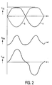
- the sensing circuit 14-16 is shown to be embodied as a main current stream maximum voltage detection circuit such that saturation is detected by detecting the maximum voltage on either one of the collectors 6 and 7, which maximum voltage Vce approaches Vcc, thus showing saturation symptoms, elucidated in fig. 2.
- the functioning of the sensing circuit 14-16 is such that it generates a increased biasing current Ibias -see fig. 2- which is controlled by the maximum of the two output voltages on collectors 6, 7. This maximum voltage will occur in the stream containing the lowest current, and therefore the lowest input voltage.
- the increased biasing current is injected at the control input 5 of current source 4, thus increasing the tail current through current source 4 which increase will essentially only increase the current in that stream A or B, were through the highest current flows.
- the current in the other stream stays at a more or less constant value higher than zero.
- the thus further increased higher current stream pulls the corresponding collector output temporarily down during saturation.
- the result is an amplified differential voltage Vout, shown in fig. 2, which does not show saturation effects.
- Bias element 16 shown to comprise a resistor can simply be used for gain control by controlling the tail current through current source 4.
- Degeneration elements 17 and 18, comprising resistors, are used to improve linearity around the cross-over point, where conduction of one of the transistors 2, 3 is taken over by the other. This reduces third order harmonic distortion.
- the differential amplifier 1 further comprises a ripple supply voltage detecting means having a ripple control output coupled to the control input 5 of the controlled current source means 4.
- the ripple supply voltage detecting means comprises a transistor 19 connected as an emitter follower with a resistor 20 and a current source 21 connected in series to earth, whose connecting point is connected to the base 22 of transistor 19. Its emitter 23 is connected to earth through a series arrangement of resistor 24 and junction 25. The connecting point of 24 and 25 is connected to the base 26 of transistor 27, whose mirrored main current stream is connected to control input 5.
- the functioning of the ripple supply voltage detecting means 19-27 is such that it reduces the bias current dependence on the power supply voltage Vcc, since any change in the supply voltage across the differential amplifier 1 results in a corresponding change in base current to transistor 4, leaving uninfluenced the biasing current through resistor 16.
- Fig. 3 shows a further embodiment of the differential amplifier according to the invention, wherein the controlled current source means comprises two separate current source semiconductors 4-1 and 4-2, whose respective biasing currents are now voltage controlled by at wish only one Vbias on the interconnected respective bases 28 and 29 of the semiconductors 4-1 and 4-2.
- Fig. 4 shows a further worked out embodiment of the differential amplifier 1.
- Extra circuitry is added therein to lower the third harmonic distortion with 3 dB.
- the circuitry essentially comprises two current sources 30 and 31 controlled by parallel input transistors 32 and 33 thus providing additional control to current source 4 for improving linearity at the cross over point mentioned earlier.
- Bias element 16 now comprises a parallel arrangement of a resistor 41 and a capacitor 34 for improving speed control characteristics.
- the differential amplifier 1 can be implemented in an IC for application in a telecommunication device such as a telephone 35 as shown in fig. 5.
- a telephone can be a mobile telephone or a fixed telephone or the like and can be implemented in a telecommunication system 36. It contains a microprocessor 37, an associated memory 38, display screen 39, and a keyboard 40.
- the telephone 35 will comprise all further features properly implemented and necessary for the required functioning thereof, together with additional features such as hands free capabilities, listening in features, loudspeaker facilities, dialling features, charging facilities etcetera.
Landscapes
- Engineering & Computer Science (AREA)
- Power Engineering (AREA)
- Amplifiers (AREA)
Claims (8)
- Differenzverstärker, der Folgendes umfasst:Differenzhauptstromzweige, jeweils mit einem Ausgang zur Erzeugung einer Ausgangsspannung,ein gesteuertes Stromquellenmittel, um einen Differenzhauptstrom in die Hauptstromzweige einzuspeisen, wobei das gesteuerte Stromquellenmittel einen Steuereingang zur Steuerung des Differenzhauptstroms hat, undeine Schleifenschaltung, die zwischen die Hauptstromzweige und den Steuereingang geschaltet ist, dadurch gekennzeichnet, dass die Schleifenschaltung eine Sättigungserfassungsschaltung umfasst, um in Abhängigkeit von der in mindestens einem der Hauptstromzweige erfassten Sättigung ein Steuereingangssignal zu erzeugen, wobei die Sättigungserfassungsschaltung eine Detektionsschaltung für die maximale Ausgangsspannung des Hauptstromzweigs ist, um Sättigungseffekte zu erfassen, indem das Annähern der Ausgangsspannung an eine Versorgungsspannung detektiert wird.
- Differenzverstärker nach Anspruch 1, dadurch gekennzeichnet, dass die Detektionsschaltung für die Maximalspannung des Hauptstromzweigs Halbleiter in Kollektorschaltung umfasst.
- Differenzverstärker nach einem der Ansprüche 1 bis 2, dadurch gekennzeichnet, dass der Differenzverstärker ein Vorspannungselement umfasst, das zwischen die Hauptstromzweige und den Steuereingang des gesteuerten Stromquellenmittels geschaltet ist.
- Differenzverstärker nach einem der Ansprüche 1 bis 3, dadurch gekennzeichnet, dass der Differenzverstärker Degenerationselemente umfasst, die in den Differenzhauptstromzweigen enthalten sind.
- Differenzverstärker nach einem der Ansprüche 1 bis 4, dadurch gekennzeichnet, dass das gesteuerte Stromquellenmittel separate gesteuerte Stromquellen hat, die jeweils mit einem entsprechenden Differenzhauptstromzweig verbunden sind (Figur 3).
- Differenzverstärker nach einem der Ansprüche 1 bis 5, dadurch gekennzeichnet, dass der Differenzverstärker Brumm-Versorgungsspannungsdetektionsmittel mit einem Brumm-Steuerausgang umfasst, der mit dem Steuereingang des gesteuerten Stromquellenmittels gekoppelt ist.
- Integrierte Schaltung mit einem Differenzverstärker nach einem der Ansprüche 1 bis 6.
- Telefon mit einer integrierten Schaltung nach Anspruch 7.
Priority Applications (1)
| Application Number | Priority Date | Filing Date | Title |
|---|---|---|---|
| EP98910955A EP0919082B1 (de) | 1997-06-25 | 1998-04-16 | Differenzverstärker, integrierte schaltung und telefon |
Applications Claiming Priority (4)
| Application Number | Priority Date | Filing Date | Title |
|---|---|---|---|
| EP97201944 | 1997-06-25 | ||
| EP97201944 | 1997-06-25 | ||
| PCT/IB1998/000572 WO1998059416A1 (en) | 1997-06-25 | 1998-04-16 | A differential amplifier, an integrated circuit, and a telephone |
| EP98910955A EP0919082B1 (de) | 1997-06-25 | 1998-04-16 | Differenzverstärker, integrierte schaltung und telefon |
Publications (2)
| Publication Number | Publication Date |
|---|---|
| EP0919082A1 EP0919082A1 (de) | 1999-06-02 |
| EP0919082B1 true EP0919082B1 (de) | 2004-01-21 |
Family
ID=8228482
Family Applications (1)
| Application Number | Title | Priority Date | Filing Date |
|---|---|---|---|
| EP98910955A Expired - Lifetime EP0919082B1 (de) | 1997-06-25 | 1998-04-16 | Differenzverstärker, integrierte schaltung und telefon |
Country Status (6)
| Country | Link |
|---|---|
| US (1) | US5999050A (de) |
| EP (1) | EP0919082B1 (de) |
| JP (1) | JP2000516789A (de) |
| CN (1) | CN1166054C (de) |
| DE (1) | DE69821197T2 (de) |
| WO (1) | WO1998059416A1 (de) |
Families Citing this family (10)
| Publication number | Priority date | Publication date | Assignee | Title |
|---|---|---|---|---|
| JP2001320243A (ja) * | 2000-05-12 | 2001-11-16 | Sony Corp | バイアス回路およびこれを用いた無線通信装置 |
| IL144811A (en) * | 2000-08-11 | 2005-12-18 | Ibm | Amplifier with suppression of harmonics |
| US7190712B2 (en) * | 2001-05-18 | 2007-03-13 | Global Locate, Inc | Method and apparatus for performing signal correlation |
| US6888406B2 (en) * | 2002-08-12 | 2005-05-03 | Microtune (Texas), L.P. | Highly linear variable gain amplifier |
| US6879534B2 (en) * | 2002-11-01 | 2005-04-12 | Hewlett-Packard Development Company, L.P. | Method and system for minimizing differential amplifier power supply sensitivity |
| DE102004024082A1 (de) * | 2004-05-14 | 2005-12-08 | Infineon Technologies Ag | Eingangsschaltung zum Empfangen eines Eingangssignals sowie ein Verfahren zum Anpassen eines Arbeitspunktes einer Eingangsschaltung |
| FR2872648B1 (fr) * | 2004-06-30 | 2006-09-08 | St Microelectronics Sa | Amplificateur a transconductance rapide |
| CN103546107A (zh) * | 2013-10-25 | 2014-01-29 | 苏州贝克微电子有限公司 | 一种宽带线性载流放大器 |
| US9391577B2 (en) * | 2014-05-07 | 2016-07-12 | Linear Technology Corporation | Low-voltage analog variable gain amplifier with enhanced linearity |
| US10848109B2 (en) | 2017-01-26 | 2020-11-24 | Analog Devices, Inc. | Bias modulation active linearization for broadband amplifiers |
Family Cites Families (5)
| Publication number | Priority date | Publication date | Assignee | Title |
|---|---|---|---|---|
| US3440554A (en) * | 1966-09-14 | 1969-04-22 | Burr Brown Res Corp | Differential dc amplifier |
| US4272728A (en) * | 1979-08-28 | 1981-06-09 | Rca Corporation | Differential-input amplifier circuit |
| US4442408A (en) * | 1982-05-13 | 1984-04-10 | International Business Machines Corporation | Differential amplifier with auto bias adjust |
| GB9019178D0 (en) * | 1990-09-03 | 1990-10-17 | Lsi Logic Europ | Power amplifiers |
| US5287071A (en) * | 1992-11-20 | 1994-02-15 | Harris Corporation | Amplifier with high common mode rejection |
-
1998
- 1998-04-16 WO PCT/IB1998/000572 patent/WO1998059416A1/en not_active Ceased
- 1998-04-16 EP EP98910955A patent/EP0919082B1/de not_active Expired - Lifetime
- 1998-04-16 CN CNB988012197A patent/CN1166054C/zh not_active Expired - Fee Related
- 1998-04-16 DE DE69821197T patent/DE69821197T2/de not_active Expired - Fee Related
- 1998-04-16 JP JP10529411A patent/JP2000516789A/ja active Pending
- 1998-06-24 US US09/103,456 patent/US5999050A/en not_active Expired - Fee Related
Also Published As
| Publication number | Publication date |
|---|---|
| CN1166054C (zh) | 2004-09-08 |
| EP0919082A1 (de) | 1999-06-02 |
| CN1237287A (zh) | 1999-12-01 |
| US5999050A (en) | 1999-12-07 |
| WO1998059416A1 (en) | 1998-12-30 |
| DE69821197D1 (de) | 2004-02-26 |
| DE69821197T2 (de) | 2004-12-02 |
| JP2000516789A (ja) | 2000-12-12 |
Similar Documents
| Publication | Publication Date | Title |
|---|---|---|
| US5699015A (en) | Low voltage operational amplifier and method | |
| US4586000A (en) | Transformerless current balanced amplifier | |
| US5150076A (en) | Emitter-grounded amplifier circuit with bias circuit | |
| US5798673A (en) | Low voltage operational amplifier bias circuit and method | |
| US4636744A (en) | Front end of an operational amplifier | |
| EP0919082B1 (de) | Differenzverstärker, integrierte schaltung und telefon | |
| SU1103812A3 (ru) | Усилитель с регулируемым коэффициентом усилени | |
| IE51754B1 (en) | Amplifier arrangement | |
| EP0730345B1 (de) | Schaltung mit variabler Verstärkung | |
| US4463319A (en) | Operational amplifier circuit | |
| US5166636A (en) | Dynamic biasing for class a amplifier | |
| US6903609B2 (en) | Operational amplifier | |
| US4163908A (en) | Bias circuit for complementary transistors | |
| US3947645A (en) | Demultiplexer for FM stereophonic receivers | |
| JP4215951B2 (ja) | 検波回路 | |
| US4945314A (en) | Amplifier arrangement with saturation detection | |
| US5376900A (en) | Push-pull output stage for amplifier in integrated circuit form | |
| CA1210089A (en) | Current source circuit arrangement | |
| GB1513448A (en) | Single-ended to push-pull converter | |
| FI74367C (fi) | Foerstaerkningsreglerad foerstaerkare med variabel emitterdegeneration. | |
| US4167649A (en) | Current mirror circuit and apparatus for using same | |
| US5122759A (en) | Class-A differential amplifier and method | |
| JPS6315766B2 (de) | ||
| US3873932A (en) | Gain control circuit having variable impedance to determine circuit gain and to control minimum gain | |
| JPH0786843A (ja) | 増幅回路 |
Legal Events
| Date | Code | Title | Description |
|---|---|---|---|
| PUAI | Public reference made under article 153(3) epc to a published international application that has entered the european phase |
Free format text: ORIGINAL CODE: 0009012 |
|
| AK | Designated contracting states |
Kind code of ref document: A1 Designated state(s): DE FR GB |
|
| 17P | Request for examination filed |
Effective date: 19990630 |
|
| 17Q | First examination report despatched |
Effective date: 20020722 |
|
| GRAH | Despatch of communication of intention to grant a patent |
Free format text: ORIGINAL CODE: EPIDOS IGRA |
|
| GRAS | Grant fee paid |
Free format text: ORIGINAL CODE: EPIDOSNIGR3 |
|
| GRAA | (expected) grant |
Free format text: ORIGINAL CODE: 0009210 |
|
| AK | Designated contracting states |
Kind code of ref document: B1 Designated state(s): DE FR GB |
|
| REG | Reference to a national code |
Ref country code: GB Ref legal event code: FG4D |
|
| REF | Corresponds to: |
Ref document number: 69821197 Country of ref document: DE Date of ref document: 20040226 Kind code of ref document: P |
|
| PGFP | Annual fee paid to national office [announced via postgrant information from national office to epo] |
Ref country code: FR Payment date: 20040427 Year of fee payment: 7 |
|
| PGFP | Annual fee paid to national office [announced via postgrant information from national office to epo] |
Ref country code: GB Payment date: 20040429 Year of fee payment: 7 |
|
| PGFP | Annual fee paid to national office [announced via postgrant information from national office to epo] |
Ref country code: DE Payment date: 20040615 Year of fee payment: 7 |
|
| ET | Fr: translation filed | ||
| PLBE | No opposition filed within time limit |
Free format text: ORIGINAL CODE: 0009261 |
|
| STAA | Information on the status of an ep patent application or granted ep patent |
Free format text: STATUS: NO OPPOSITION FILED WITHIN TIME LIMIT |
|
| 26N | No opposition filed |
Effective date: 20041022 |
|
| PG25 | Lapsed in a contracting state [announced via postgrant information from national office to epo] |
Ref country code: GB Free format text: LAPSE BECAUSE OF NON-PAYMENT OF DUE FEES Effective date: 20050416 |
|
| PG25 | Lapsed in a contracting state [announced via postgrant information from national office to epo] |
Ref country code: DE Free format text: LAPSE BECAUSE OF NON-PAYMENT OF DUE FEES Effective date: 20051101 |
|
| GBPC | Gb: european patent ceased through non-payment of renewal fee |
Effective date: 20050416 |
|
| PG25 | Lapsed in a contracting state [announced via postgrant information from national office to epo] |
Ref country code: FR Free format text: LAPSE BECAUSE OF NON-PAYMENT OF DUE FEES Effective date: 20051230 |
|
| REG | Reference to a national code |
Ref country code: FR Ref legal event code: ST Effective date: 20051230 |