EP0917412B1 - Self-oscillating circuit with simplified startup circuit - Google Patents
Self-oscillating circuit with simplified startup circuit Download PDFInfo
- Publication number
- EP0917412B1 EP0917412B1 EP98119611A EP98119611A EP0917412B1 EP 0917412 B1 EP0917412 B1 EP 0917412B1 EP 98119611 A EP98119611 A EP 98119611A EP 98119611 A EP98119611 A EP 98119611A EP 0917412 B1 EP0917412 B1 EP 0917412B1
- Authority
- EP
- European Patent Office
- Prior art keywords
- circuit
- capacitor
- bridge
- transistor
- resistor
- Prior art date
- Legal status (The legal status is an assumption and is not a legal conclusion. Google has not performed a legal analysis and makes no representation as to the accuracy of the status listed.)
- Expired - Lifetime
Links
Images


Classifications
-
- H—ELECTRICITY
- H05—ELECTRIC TECHNIQUES NOT OTHERWISE PROVIDED FOR
- H05B—ELECTRIC HEATING; ELECTRIC LIGHT SOURCES NOT OTHERWISE PROVIDED FOR; CIRCUIT ARRANGEMENTS FOR ELECTRIC LIGHT SOURCES, IN GENERAL
- H05B41/00—Circuit arrangements or apparatus for igniting or operating discharge lamps
- H05B41/14—Circuit arrangements
- H05B41/26—Circuit arrangements in which the lamp is fed by power derived from dc by means of a converter, e.g. by high-voltage dc
- H05B41/28—Circuit arrangements in which the lamp is fed by power derived from dc by means of a converter, e.g. by high-voltage dc using static converters
- H05B41/282—Circuit arrangements in which the lamp is fed by power derived from dc by means of a converter, e.g. by high-voltage dc using static converters with semiconductor devices
- H05B41/2825—Circuit arrangements in which the lamp is fed by power derived from dc by means of a converter, e.g. by high-voltage dc using static converters with semiconductor devices by means of a bridge converter in the final stage
-
- Y—GENERAL TAGGING OF NEW TECHNOLOGICAL DEVELOPMENTS; GENERAL TAGGING OF CROSS-SECTIONAL TECHNOLOGIES SPANNING OVER SEVERAL SECTIONS OF THE IPC; TECHNICAL SUBJECTS COVERED BY FORMER USPC CROSS-REFERENCE ART COLLECTIONS [XRACs] AND DIGESTS
- Y02—TECHNOLOGIES OR APPLICATIONS FOR MITIGATION OR ADAPTATION AGAINST CLIMATE CHANGE
- Y02B—CLIMATE CHANGE MITIGATION TECHNOLOGIES RELATED TO BUILDINGS, e.g. HOUSING, HOUSE APPLIANCES OR RELATED END-USER APPLICATIONS
- Y02B20/00—Energy efficient lighting technologies, e.g. halogen lamps or gas discharge lamps
-
- Y—GENERAL TAGGING OF NEW TECHNOLOGICAL DEVELOPMENTS; GENERAL TAGGING OF CROSS-SECTIONAL TECHNOLOGIES SPANNING OVER SEVERAL SECTIONS OF THE IPC; TECHNICAL SUBJECTS COVERED BY FORMER USPC CROSS-REFERENCE ART COLLECTIONS [XRACs] AND DIGESTS
- Y10—TECHNICAL SUBJECTS COVERED BY FORMER USPC
- Y10S—TECHNICAL SUBJECTS COVERED BY FORMER USPC CROSS-REFERENCE ART COLLECTIONS [XRACs] AND DIGESTS
- Y10S315/00—Electric lamp and discharge devices: systems
- Y10S315/05—Starting and operating circuit for fluorescent lamp
Definitions
- This invention relates to an operating circuit for a low pressure gas discharge lamp with a rectifier, with a free-swinging half bridge with voltage controlled field effect or IGBT transistors for generation a high frequency output power for the low pressure gas discharge lamp a supply power and with a start-up circuit for starting the free-swinging Oscillation with one between a drive circuit on one Control connection of a field effect or IGBT transistor and a reference potential of the field effect or IGBT transistor switched starting capacitor.
- Diacs compared to other components used in the operational circuits an above average show high failure rates and thus unnecessarily high failure rates of the electronic ballasts or other operating circuits equipped with them to lead.
- the starting capacitor does the job with increasing charging through its connector to a reference potential of a switching element, such as a power supply branch, after switching on the power supply a control circuit of the To enable the oscillator or one of its switching elements, a first Switching operation of the relevant switching element.
- a switching element such as a power supply branch
- a first Switching operation of the relevant switching element is the case with voltage-controlled switching elements no very high currents, just a certain voltage is required.
- Voltage-controlled switching elements have with regard to their switching on or off basically a defined threshold voltage.
- the diode with your Breakthrough process, which the invention is intended to avoid, as explained, can therefore be replaced are approached by and exceeding the voltage threshold of the switching element. This process is accomplished by switching on the power supply charging starting capacitor directly or indirectly.
- Charging the starting capacitor should be easy via one between the starting capacitor and a potential suitable for charging, such as a power supply branch, switched charging resistor take place, the relatively high resistance should be dimensioned so that the start-up circuit interferes little in oscillation mode.
- a corresponding circuit is known from US Pat. No. 5,592,367, in which the charging resistor is connected on the DC side of the rectifier bridge. at However, this circuit may have a current flowing across the charging resistor with a current-carrying connection of the FET transistor connecting diode and the still slightly conductive FET transistor that flows exactly over the current compensated for the starting capacitor. In this case, the current can flow through the starting capacitor no longer bring the FET transistor into the conductive state, so that a new starting process of the circuit arrangement only due to an interruption in the network can be achieved.
- the object of the invention is therefore this disadvantage through an improved start-up circuit to get around.
- the invention provides an operating circuit for a low-pressure gas discharge lamp with the features listed in the preamble of claim 1 before, which is characterized by a between the starting capacitor and a mains input side of the rectifier switched charging resistor and one discharge resistor connected in parallel with the starting capacitor.
- From US 5 140 225 is the connection of a starting circuit via a resistor known on the AC side of the rectifier.
- connections are supposed to be the power loss during charging of the starting capacitor be reduced.
- the starting capacitor connected in parallel in the circuit arrangement from US Pat. No. 5,592,367 Diode cannot contribute to the discharge resistor connected in parallel be compared to the present circuit because the diode has the wrong polarity for discharging the starting capacitor.
- An advantageous embodiment of the invention consists in a discharge diode for cyclical discharge of the starting capacitor in oscillation mode. Is the free-swinging Once the oscillation of the operating circuit has started, step on on the other connection side of the discharge diode with the oscillation frequency Potential states on the starting capacitor cyclically via the discharge diode discharged.
- the discharge diode blocks in other potential states. It is preferred between the control circuit side connection of the starting capacitor and the connection of the switching element remote from the supply branch, in the case of a bridge circuit a center tap of the bridge.
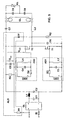
- FIG. 1 shows an operating circuit in an electronic ballast for a low-pressure gas discharge lamp, which is shown as load EL.
- a rectifier GL with mains voltage is used via a fuse SI supplied, which feeds an electrolytic capacitor C1 or keeps it live.
- Two supply branches are tapped at the electrolytic capacitor C1 via a filter from a coil L1 in one of the branches and one both Capacitor C2 connecting branches.
- the lower supply branch in the figure has negative potential and defines the reference potential on the rectified side of the operating circuit.
- the upper is the supply branch that is positive.
- a half bridge made up of two MOSFET transistors is located in both supply branches T1 and T2, with N-channel transistors each on the negative Side source connector are used.
- a load circuit consisting of a load series lamp choke L2, the low pressure gas discharge lamp EL and the load serial coupling capacitor C7.
- control circuit AS1 or AS2 Between the source terminal of the MOSFET transistors T1 and T2 as internal transistor reference potential and the respective gate terminal one control circuit AS1 or AS2. With the lower half-bridge transistor T1 is the control circuit AS1, however, via the following Start-up circuit ALS described in more detail with the source connection of the Transistor T1 connected.
- the control circuits AS1 and AS2 are identical constructed and consist of a parallel connection of a coil L3 or L4, a capacitor C3 or C4 and a series connection of a secondary winding HW1 or HW2 of a control transformer, its primary winding the lamp choke already mentioned is L2, and a resistor R3 or R4.
- the winding sense of the secondary windings is - how indicated by the points on HW1, HW2 and L2 - opposite to each other.
- the starting circuit In the lower area in FIG. 1 is the starting circuit with a dashed line ALS summarized, but basically also a resistance R2 between the center tap of the half-bridge and the positive Supply branch belongs.
- a starting capacitor C5 In the start-up circuit is initially a starting capacitor C5 between the drive circuit AS1 of the lower one Bridge transistor T1 and the negative supply branch.
- a discharge resistor R5. Are in series with the starting capacitor C5 a discharge diode in connection with the center tap of the half-bridge D1 with its anode on the part of the starting capacitor C5, and a charging resistor R1 in connection with an AC voltage connection on the input side of the rectifier GL.
- the resistor R2 keeps the center tap of the half-bridge at the potential of the positive supply branch. This means that virtually the entire DC voltage of the electrolytic capacitor C1 is present at the lower bridge transistor T1. It is essential that the voltage U C5 on the starting capacitor C5 with the voltage of the drive circuit 1, that is the voltage on the capacitor C3, added between the source connection and the gate connection of the bridge transistor T1, is present in the figure as U GS .
- the control circuits AS1 and AS2 In the absence of positive feedback by the control transformer L2-HW1 / HW2 and in the absence of potential oscillation at the center of the half-bridge, the control circuits AS1 and AS2 initially do not give an output signal, so that the start-up circuit ALS must take care of a first switching operation.
- the bridge transistor T1 is switched on for the first time by charging the starting capacitor C5 via the charging resistor R1 on the part of a power supply line.
- the current in the lamp inductor L2 starts the positive feedback mechanism by generating an induction current in the secondary windings HW1 and HW2 in accordance with the turn ratio on this lamp inductor L2.
- the now conductive transistor T1 discharges together with the discharge diode D1 - the bridge center potential drops - the starting capacitor C5, however, the induction current in the secondary winding HW1 charges the capacitor C3 via the resistor R3 and thus keeps the transistor T1 switched on. If the first turn-on of the bridge transistor T1 by the voltage U C5 at the starting capacitor C5 has generated sufficient conductivity in the transistor T1, the free-oscillation now starts via the positive feedback mechanism and reaches a steady state over a few periods.
- the potential oscillation at the center of the bridge cyclically discharges the starting capacitor C5 via the discharge diode D1 and thus keeps the voltage U C5 negligibly small.
- the charging resistor R1 is connected to a power line on the input side of the rectifier GL. This has the following background: It is to be avoided with certainty that a steady state over several mains half-waves, which can occur, for example, when the load current breaks off for a short time for reasons lying in the lamp EL and thus the positive feedback is interrupted and the voltage U C5 is equal to the switch-on threshold voltage of the bridge transistor T1.
- the total discharge current via the discharge diode D1 and the bridge transistor T1 compensates for the current charging the starting capacitor C5 and flowing through the charging resistor R after the steady state has been reached.
- the bridge midpoint potential would have been almost pulled down to the potential of the negative supply branch due to the low conductivity of the transistor T1, so that the voltage across the electrolytic capacitor C1 would essentially correspond to the total voltage across the capacitors C7, C8 and C9 of the load circuit.
- the drain-source voltage at transistor T1 would then be practically equal to the gate-source voltage U GS .
- the starting process described above with reference to the circuit diagram in FIG. 1 is shown in another way in FIG. 2 by means of the gate-source voltage U GS of the transistor T1, the voltage U C5 at the starting capacitor C5, the current I T1 through the bridge transistor T1 ( over the switched path) and the current I L2 through the lamp choke L2.
- the time axis runs from left to right, and the deviating zero points for the voltages and currents are shown on the left edge of the figure.
- the charging process that is to say the rise in voltage U C5 over time
- the figure begins after a simultaneous increase in the voltages U C5 and U GS when the switch-on threshold voltage of the transistor T1 is exceeded, which is manifested in the sudden increase in the current I T1 .
- the short current peak results from the rapid charging of the trapezoidal capacitor C6, but the rise in I T1 continues afterwards.
- the rise in the transistor current I T1 is reflected to a certain extent in a dip in the voltage U C5.
- the diagram in FIG. 2 shows how the lamp inductor current I L2 is started when the conductivity of the transistor T1 begins, that is to say by I T1 .
- the positive feedback mechanism described already leads to the start of the activity of the control circuits when the transistor current L T1 rises, ie the transistor T1 is switched off again by the control circuit AS1 and the transistor T2 is subsequently switched on by the control circuit AS2. Accordingly, the voltage U GS on the transistor T1 oscillates through to negative values, which in turn manifests itself in the beginning oscillation of the lamp inductor current I L2 . In the further course of time, oscillations oscillating both of the voltage U GS and of the load or lamp inductor current I L2 can be seen .
- the second dip in voltage U C5 at starting capacitor C5 is significantly stronger than the first, albeit of a similar quality.
- the quantitative increase in the effect is due to the much clearer conductivity of the bridge transistor T1 in the second or first switch-on process purely caused by the positive feedback mechanism.
- the potential of the center of the bridge falls below the reference potential of the negative supply branch, namely because of the forward voltage of the body diode of the MOSFET T1, which must now conduct the considerable current flow from the lamp inductor L2.
- the second embodiment whose Circuit diagram shown in Figure 3.
- the differences from the circuit Figure 1 are as follows:
- the bridge transistor T2 is now a P-channel MOSFET instead of the previous N-channel MOSFET.
- the resistance is accordingly R2 now between the bridge center and the negative Supply branch.
- the control circuit AS2 is not at the bridge center but connected to the positive, upper supply branch.
- the start-up circuit can - and this embodiment serves this purpose ALS now between the control circuit AS2 and the positive Supply branch must be switched.
- the charging resistance R1 is present here the other mains lead.
- the polarity of the discharge diode D1 is adjusted, vice versa.
- capacitor C6 is also between the bridge center and the lower, i.e. negative supply branch; however, it could just as well be in the old place.
- the Functioning otherwise corresponds to that described above and will not explained again here.
- control circuits AS1 and AS2 also from a parallel connection of only one capacitor C3, C4 and a series connection of a resistor R3, R4 and a secondary winding HW1, HW2 of a control transformer, its primary winding the lamp choke listed above is L2. Otherwise the circuit structure is identical to the circuit shown in FIG. 1.
Description
Diese Erfindung bezieht sich auf eine Betriebsschaltung für eine Niederdruck-Gasentladungslampe mit einem Gleichrichter, mit einer freischwingenden Halbbrücke mit spannungsgesteuerten Feldeffekt- oder IGBT-Transistoren zur Erzeugung einer Hochfrequenzausgangsleistung für die Niederdruck-Gasentladungslampe aus einer Versorgungsleistung und mit einer Anlaufschaltung zum Ingangsetzen der freischwingenden Oszillation mit einem zwischen eine Ansteuerschaltung an einem Steueranschluss eines Feldeffekt- oder IGBT-Transistors und ein Bezugspotential des Feldeffekt- oder IGBT-Transistors geschalteten Anlaufkondensator.This invention relates to an operating circuit for a low pressure gas discharge lamp with a rectifier, with a free-swinging half bridge with voltage controlled field effect or IGBT transistors for generation a high frequency output power for the low pressure gas discharge lamp a supply power and with a start-up circuit for starting the free-swinging Oscillation with one between a drive circuit on one Control connection of a field effect or IGBT transistor and a reference potential of the field effect or IGBT transistor switched starting capacitor.
Ein für diese Erfindung wichtiger Gesichtspunkt solcher Betriebsschaltungen resultiert aus der Notwendigkeit, die freischwingende Oszillation des Oszillators beim Betriebsstart in Gang zu setzen. Häufig werden zur Erzeugung der freischwingenden Oszillation z. B. mitkoppelnde Steuertransformatoren zur Ansteuerung der Schaltelemente des Oszillators verwendet. Der Mitkopplungseffekt entsteht jedoch erst im Oszillationsbetrieb selbst und muss zu Anfang sozusagen durch einen äußeren Anstoß erst erzeugt werden.An important aspect of such operating circuits for this invention results from the need to control the free oscillation of the oscillator Start the operation. Often used to generate the free-swinging Oscillation e.g. B. coupled-in control transformers for controlling the switching elements of the oscillator used. The positive feedback effect only arises in the Oscillation operation itself and has to be started by an external impulse be created first.
Eine bekannte Lösung für eine Anlaufschaltung, die diesen Anstoß beim Einschalten der Versorgungsleistung erzeugt, kann der deutschen Anmeldung DE 195 48 506 A1 entnommen werden. Dabei wird nach Einschalten der Versorgungsleistung ein Kondensator über einen Widerstand so lange aufgeladen, bis die Durchbruchspannung eines Diac erreicht ist. Dessen Durchbruch entlädt einen Teil der in dem Kondensator gespeicherten Ladung in eine Ansteuerschaltung eines Feldeffekttransistors eines Halbbrückenoszillators. Weitere Einzelheiten sind dem zitierten Dokument zu entnehmen.A known solution for a start-up circuit that initiates this when switched on the supply power generated, the German application DE 195 48 506 A1 be removed. After switching on the supply power, a capacitor becomes charged through a resistor until the breakdown voltage a diac is reached. Its breakthrough discharges part of that in the capacitor stored charge in a drive circuit of a field effect transistor Half-bridge oscillator. Further details can be found in the cited document.
Der im Stand der Technik verwendete Diac stellt einen wesentlichen Nachteil der konventionellen Lösung dar. Es hat sich nämlich gezeigt, dass Diacs im Vergleich zu anderen in den Betriebsschaltungen verwendeten Bauelementen eine überdurchschnittlich hohe Ausfallrate zeigen und damit zu unnötig hohen Ausfallraten der mit ihnen ausgestatteten elektronischen Vorschaltgeräte bzw. anderer Betriebsschaltungen führen.The diac used in the prior art is a major disadvantage of conventional solution. It has been shown that Diacs compared to other components used in the operational circuits an above average show high failure rates and thus unnecessarily high failure rates of the electronic ballasts or other operating circuits equipped with them to lead.
Es wird deswegen auf die Verwendung eines Diacs verzichtet. Statt dessen ist ein Kondensator vorgesehen, der hier als Anlaufkondensator bezeichnet wird. Der Anlaufkondensator hat die Aufgabe, bei zunehmender Aufladung durch seinen Anschluss an ein Bezugspotential eines Schaltelements, etwa ein Leistungsversorgungszweig, nach dem Einschalten der Leistungsversorgung eine Ansteuerschaltung des Oszillators bzw. eines seiner Schaltelemente in die Lage zu versetzen, einen ersten Schaltvorgang des betreffenden Schaltelements hervorzurufen. Dabei ist insbesondere daran zu denken, dass bei spannungsgesteuerten Schaltelementen hierzu keine sehr hohen Ströme, sondern lediglich eine gewisse Spannung erforderlich ist. Spannungsgesteuerte Schaltelemente haben hinsichtlich ihres Ein- oder Ausschaltvorgangs grundsätzlich eine definierte Schwellenspannung. Die Diode mit ihrem Durchbruchvorgang, die die Erfindung, wie erläutert, vermeiden soll, kann also ersetzt werden durch Heranfahren an den und Überschreiten des Spannungsschwellenwerts des Schaltelements. Dieser Vorgang wird durch den beim Einschalten der Leistungsversorgung sich aufladenden Anlaufkondensator direkt oder indirekt bewirkt.Therefore, the use of a diac is avoided. Instead is a Capacitor provided, which is referred to here as the starting capacitor. The starting capacitor does the job with increasing charging through its connector to a reference potential of a switching element, such as a power supply branch, after switching on the power supply a control circuit of the To enable the oscillator or one of its switching elements, a first Switching operation of the relevant switching element. Here is particular remember that this is the case with voltage-controlled switching elements no very high currents, just a certain voltage is required. Voltage-controlled switching elements have with regard to their switching on or off basically a defined threshold voltage. The diode with your Breakthrough process, which the invention is intended to avoid, as explained, can therefore be replaced are approached by and exceeding the voltage threshold of the switching element. This process is accomplished by switching on the power supply charging starting capacitor directly or indirectly.
Dies kann beispielsweise dadurch geschehen, dass das Potential einer komplexeren Ansteuerschaltung, auf die im folgenden näher eingegangen wird, insgesamt durch den Anlaufkondensator verschoben wird. Es ist aber nicht unbedingt notwendig, eine komplexere Ansteuerschaltung vorzusehen; vielmehr kann im einfachsten Fall hier auch nur ein Anschlusspunkt einer wie auch immer gearteten Mitkopplungseinrichtung für die freischwingende Oszillation (etwa der Sekundärwicklung eines Steuertransformators) als "Ansteuerschaltung" im Minimalsinn vorgesehen sein, so dass die an dem Anlaufkondensator anliegende Spannung praktisch unmittelbar an den Steueranschluss des spannungsgesteuerten Schaltelements angreift. Diese einfachen "Minimalversionen" für eine Ansteuerschaltung könnte man sich im Fall des Steuertransformators beispielsweise dann vorstellen, wenn die Primärwicklung bereits mit der richtigen Phasenverzögerung für die Ansteuerung der Schaltelemente beaufschlagt wird.This can happen, for example, in that the potential of a more complex one Control circuit, which will be discussed in more detail below, by the starting capacitor is shifted. But it is not absolutely necessary to have one to provide more complex control circuit; rather, in the simplest case, here even just a connection point of a positive feedback device of any kind for free oscillation (e.g. the secondary winding of a control transformer) be provided as a "control circuit" in the minimal sense, so that the voltage applied to the starting capacitor practically directly to the Control connection of the voltage-controlled switching element attacks. These simple ones "Minimal versions" for a control circuit could be found in the case of the control transformer For example, imagine if the primary winding is already with the correct phase delay for driving the switching elements becomes.
Jedenfalls ist die Verwendung eines Anlaufkondensators als einfaches und preiswertes Bauelement vorgesehen, wodurch der Diac mit den beschriebenen Nachteilen überflüssig ist.In any case, the use of a starting capacitor is simple and inexpensive Component provided, whereby the diac with the disadvantages described is superfluous.
Das Aufladen des Anlaufkondensators sollte einfach über einen zwischen den Anlaufkondensator und ein zum Aufladen geeignetes Potential, etwa einen Leistungsversorgungszweig, geschalteten Aufladewiderstand erfolgen, der relativ hochohmig bemessen sein sollte, damit die Anlaufschaltung im Oszillationsbetrieb wenig stört.Charging the starting capacitor should be easy via one between the starting capacitor and a potential suitable for charging, such as a power supply branch, switched charging resistor take place, the relatively high resistance should be dimensioned so that the start-up circuit interferes little in oscillation mode.
Aus der US 5 592 367 ist eine entsprechende Schaltung bekannt, bei der der Aufladewiderstand auf der Gleichstromseite der Gleichrichterbrücke angeschlossen ist. Bei dieser Schaltung kann jedoch vorkommen, dass ein Strom über eine den Aufladewiderstand mit einem stromführenden Anschluss des FET-Transistors verbindende Diode und den noch leicht leitenden FET-Transistor fließt, der genau den Strom über den Anlaufkondensator kompensiert. In diesem Fall kann der Strom über den Anlaufkondensator den FET-Transistor nicht mehr in den leitenden Zustand überführen, so dass ein neuer Startvorgang der Schaltungsanordnung nur durch eine Netzunterbrechung zu erzielen ist.A corresponding circuit is known from US Pat. No. 5,592,367, in which the charging resistor is connected on the DC side of the rectifier bridge. at However, this circuit may have a current flowing across the charging resistor with a current-carrying connection of the FET transistor connecting diode and the still slightly conductive FET transistor that flows exactly over the current compensated for the starting capacitor. In this case, the current can flow through the starting capacitor no longer bring the FET transistor into the conductive state, so that a new starting process of the circuit arrangement only due to an interruption in the network can be achieved.
Aufgabe der Erfindung ist es daher diesen Nachteil durch eine verbesserte Anlaufschaltung zu umgehen.The object of the invention is therefore this disadvantage through an improved start-up circuit to get around.
Dazu sieht die Erfindung eine Betriebsschaltung für eine Niederdruck-Gasentladungslampe
mit den im Oberbegriff des Anspruchs 1 aufgeführten Merkmalen
vor, die gekennzeichnet ist durch einen zwischen den Anlaufkondensator und
eine Netzeingangsseite des Gleichrichters geschalteten Aufladewiderstand und einen
parallel zu dem Anlaufkondensator geschalteten Entladewiderstand. To this end, the invention provides an operating circuit for a low-pressure gas discharge lamp
with the features listed in the preamble of
Der Anschluss des Aufladewiderstands auf der Wechselstromseite der Gleichrichterbrücke und die Parallelschaltung eines Entladewiderstands, über den der Anlaufkondensator während der "negativen" Netzhalbwellen entladen wird, vermeidet bei der vorliegenden Anmeldung einen solchen "stabilen Zustand".The connection of the charging resistor on the AC side of the rectifier bridge and the parallel connection of a discharge resistor, via which the starting capacitor while the "negative" mains half-wave is being discharged, the present application such a "stable state".
Aus der US 5 140 225 ist zwar der Anschluss einer Anlaufschaltung über einen Widerstand auf der Wechselstromseite des Gleichrichters bekannt. Durch die Art der Anschlüsse soll hier jedoch die Verlustleistung während des Aufladens des Anlaufkondensators verringert werden.From US 5 140 225 is the connection of a starting circuit via a resistor known on the AC side of the rectifier. By the nature of the However, connections are supposed to be the power loss during charging of the starting capacitor be reduced.
Die bei der Schaltungsanordnung aus der US 5 592 367 dem Anlaufkondensator parallelgeschaltete Diode kann nicht dem parallel geschalteten Entladewiderstand bei der vorliegenden Schaltung gleichgestellt werden, da die Diode die falsche Polarität zur Entladung des Anlaufkondensators aufweist.The starting capacitor connected in parallel in the circuit arrangement from US Pat. No. 5,592,367 Diode cannot contribute to the discharge resistor connected in parallel be compared to the present circuit because the diode has the wrong polarity for discharging the starting capacitor.
Eine vorteilhafte Ausgestaltung der Erfindung besteht in einer Entladediode zum zyklischen Entladen des Anlaufkondensators im Oszillationsbetrieb. Ist die freischwingende Oszillation der Betriebsschaltung erst einmal in Gang gekommen, treten auf der anderen Anschlussseite der Entladediode mit der Oszillationsfrequenz Potentialzustände auf, die den Anlaufkondensator über die Entladediode zyklisch entladen. Bei anderen Potentialzuständen sperrt die Entladediode. Sie ist vorzugsweise zwischen den ansteuerschaltungsseitigen Anschluss des Anlaufkondensators und den versorgungszweigfernen Anschluss des Schaltelements, bei einer Brückenschaltung also einen Mittelpunktsabgriff der Brücke, geschaltet.An advantageous embodiment of the invention consists in a discharge diode for cyclical discharge of the starting capacitor in oscillation mode. Is the free-swinging Once the oscillation of the operating circuit has started, step on on the other connection side of the discharge diode with the oscillation frequency Potential states on the starting capacitor cyclically via the discharge diode discharged. The discharge diode blocks in other potential states. It is preferred between the control circuit side connection of the starting capacitor and the connection of the switching element remote from the supply branch, in the case of a bridge circuit a center tap of the bridge.
Wie bereits ausgeführt sind für die konkrete Ausführung des hier allgemein verwendeten Begriffs "Ansteuerschaltung" verschiedene Möglichkeiten denkbar. Zwei bevorzugte Varianten, die sich als für einen zuverlässigen und verlustarmen Betrieb insbesondere einer Halbbrückenschaltung sehr geeignet erwiesen haben, sind die folgenden: Im ersten Fall ist in der Ansteuerschaltung einer Serienschaltung aus einem Widerstand und einer Sekundärwicklung eines Steuertransformators eine Parallelschaltung aus einem Kondensator und einer Spule parallel geschaltet, wobei die Serienschaltung und die Parallelschaltung gemeinsam an dem Steueranschluß des betreffenden Schaltelements angeschlossen sind. Dabei bildet die Parallelschaltung aus Kondensator und Spule einen Schwingkreis. Im zweiten Fall ist die dem Kondensator parallel liegende Spule weggelassen. Funktionsweise, Vorteile und weitere Varianten zu diesen beiden Formen sind folgenden Dokumenten zu entnehmen, deren Offenbarung hierzu in dieser Anmeldung eingeschlossen ist: zum einen die DE 41 29 430 A1 sowie die DE 195 48 506 A1, die bereits erwähnt wurde.As already stated, for the specific implementation of what is generally used here Different possibilities conceivable. Two preferred Variants that prove to be reliable and low-loss operation have proven to be very suitable, in particular a half-bridge circuit the following: In the first case, the control circuit of a series circuit consists of one Resistor and a secondary winding of a control transformer a parallel connection from a capacitor and a coil connected in parallel, the series circuit and the parallel connection together at the control connection of the concerned Switching element are connected. The parallel connection forms a resonant circuit consisting of capacitor and coil. In the second case it is the coil in parallel with the capacitor is omitted. How it works, advantages and further variants of these two forms are the following documents see the disclosure of which is included in this application is: on the one hand DE 41 29 430 A1 and DE 195 48 506 A1, that has already been mentioned.
Um den Potentialzustand der Betriebsschaltung vor dem Einschalten für den Anfang des Anlaufvorgangs definiert vorzugeben, kann man z. B. einen Widerstand zwischen einen versorgungszweigfernen Anschluß eines der Schaltelemente und einem Versorgungszweig vorsehen. Durch einen solchen - für einen störungsfreien Normalbetrieb natürlich hochohmigen - Widerstand liegt das Potential des betreffenden versorgungszweigfernen Anschlusses im Ruhezustand auf dem Potential des Versorgungszweiges, d. h. an bestimmten Schaltelementen liegt beim Anlaufvorgang zunächst keine Spannung oder im wesentlichen die gesamte (gleichgerichtete) Versorgungsspannung an.To the potential state of the operating circuit before switching on for the To specify the start of the start-up process, you can e.g. B. a resistor between a connection of one of the switching elements remote from the supply branch and provide a branch of supply. By such - for a trouble-free normal operation, of course, high-resistance is the potential of the relevant connection remote from the supply branch Idle state at the potential of the supply branch, d. H. on certain Switching elements are initially without voltage during the start-up process or essentially the entire (rectified) supply voltage on.
Im folgenden werden anhand der Figuren drei konkrete Ausrührungsbeispiele
für die Erfindung beschrieben, wobei die dabei offenbarten Einzelmerkmale
auch in anderen als den gezeigten Kombinationen oder einzeln
erfindungswesentlich sein können. Es zeigt:
Figur 1 zeigt eine Betriebsschaltung in einem elektronischen Vorschaltgerät für eine Niederdruck-Gasentladungslampe, die als Last EL dargestellt ist. Dabei wird über eine Sicherung SI ein Gleichrichter GL mit Netzspannung versorgt, der einen Elektrolytkondensator C1 speist bzw. auf Spannung hält. An dem Elektrolytkondensator C1 werden zwei Versorgungszweige abgegriffen über ein Filter aus einer Spule L1 in einem der Zweige und einen beide Zweige verbindenden Kondensator C2.Figure 1 shows an operating circuit in an electronic ballast for a low-pressure gas discharge lamp, which is shown as load EL. In this case, a rectifier GL with mains voltage is used via a fuse SI supplied, which feeds an electrolytic capacitor C1 or keeps it live. Two supply branches are tapped at the electrolytic capacitor C1 via a filter from a coil L1 in one of the branches and one both Capacitor C2 connecting branches.
Der in der Figur untere Versorgungszweig hat negatives Potential und definiert das Bezugspotential auf der gleichgerichteten Seite der Betriebsschaltung. Der obere ist der dem gegenüber positive Versorgungszweig. Zwischen beiden Versorgungszweigen liegt eine Halbbrücke aus zwei MOSFET-Transistoren T1 und T2, wobei N-Kanal-Transistoren mit jeweils auf der negativen Seite liegendem Source-Anschluß verwendet sind. Zwischen einem Mittelpunktsabgriff der Halbbrücke und dem positiven Versorgungszweig liegt ein Lastkreis aus einer lastseriellen Lampendrossel L2, der Niederdruck-Gasentladungslampe EL und dem lastseriellen Koppelkondensator C7. Ferner ist eine lastparallele Verschaltung mit zwei Resonanzkondensatoren C8 und C9 und einem Kaltleiter KL für die Lampenzündung vorgesehen.The lower supply branch in the figure has negative potential and defines the reference potential on the rectified side of the operating circuit. The upper is the supply branch that is positive. Between A half bridge made up of two MOSFET transistors is located in both supply branches T1 and T2, with N-channel transistors each on the negative Side source connector are used. Between one Center tap of the half-bridge and the positive supply branch there is a load circuit consisting of a load series lamp choke L2, the low pressure gas discharge lamp EL and the load serial coupling capacitor C7. Furthermore, there is a load-parallel connection with two resonance capacitors C8 and C9 and a PTC thermistor KL provided for the lamp ignition.
Zur Schaltentlastung der MOSFET-Transistoren T1 und T2 liegt dem oberen Halbbrückentransistor T2 ein Kondensator C6 parallel. To relieve the switching of the MOSFET transistors T1 and T2 is the upper one Half-bridge transistor T2 a capacitor C6 in parallel.
Zwischen dem Source-Anschluß der MOSFET-Transistoren T1 und T2 als transistorinternem Bezugspotential und dem jeweiligen Gate-Anschluß liegt jeweils eine Ansteuerschaltung AS1 bzw. AS2. Bei dem unteren Halbbrükkentransistor T1 ist die Ansteuerschaltung AS1 jedoch über die im folgenden näher beschriebene Anlaufschaltung ALS mit dem Source-Anschluß des Transistors T1 verbunden. Die Ansteuerschaltungen AS1 und AS2 sind identisch aufgebaut und bestehen aus einer Parallelschaltung einer Spule L3 bzw. L4, eines Kondensators C3 bzw. C4 und einer Serienschaltung aus einer Sekundärwicklung HW1 bzw. HW2 eines Steuertransformators, dessen Primärwicklung die bereits erwähnte Lampendrossel L2 ist, und einem Widerstand R3 bzw. R4. Der Windungssinn der Sekundärwicklungen ist - wie durch die Punkte an HW1, HW2 und L2 angedeutet - entgegengesetzt zueinander.Between the source terminal of the MOSFET transistors T1 and T2 as internal transistor reference potential and the respective gate terminal one control circuit AS1 or AS2. With the lower half-bridge transistor T1 is the control circuit AS1, however, via the following Start-up circuit ALS described in more detail with the source connection of the Transistor T1 connected. The control circuits AS1 and AS2 are identical constructed and consist of a parallel connection of a coil L3 or L4, a capacitor C3 or C4 and a series connection of a secondary winding HW1 or HW2 of a control transformer, its primary winding the lamp choke already mentioned is L2, and a resistor R3 or R4. The winding sense of the secondary windings is - how indicated by the points on HW1, HW2 and L2 - opposite to each other.
Die bisher beschriebenen Schaltungselemente sind bekannt und so auch in der bereits zitierten DE 195 48 506 A1 zu finden. Auf diese Anmeldung und den übrigen einschlägigen Stand der Technik wird wegen weiterer Einzelheiten verwiesen.The circuit elements described so far are known and thus also in to find the already cited DE 195 48 506 A1. On this registration and the rest of the relevant prior art is for further details directed.
Im unteren Bereich in Figur 1 ist mit einer gestrichelten Linie die Anlaufschaltung ALS zusammengefaßt, zu der im Grunde aber auch ein Widerstand R2 zwischen dem Mittelpunktsabgriff der Halbbrücke und dem positiven Versorgungszweig gehört. In der Anlaufschaltung befindet sich zunächst ein Anlaufkondensator C5 zwischen der Ansteuerschaltung AS1 des unteren Brückentransistors T1 und dem negativen Versorgungszweig. Parallel dazu liegt ein Entladewiderstand R5. Seriell zu dem Anlaufkondensator C5 liegen in einer Verbindung zu dem Mittelpunktsabgriff der Halbbrücke eine Entladediode D1 mit ihrer Anode auf Seiten des Anlaufkondensators C5, sowie ein Aufladewiderstand R1 in einer Verbindung zu einem Wechselspannungsanschluß auf der Eingangsseite des Gleichrichters GL. In the lower area in FIG. 1 is the starting circuit with a dashed line ALS summarized, but basically also a resistance R2 between the center tap of the half-bridge and the positive Supply branch belongs. In the start-up circuit is initially a starting capacitor C5 between the drive circuit AS1 of the lower one Bridge transistor T1 and the negative supply branch. In parallel there is a discharge resistor R5. Are in series with the starting capacitor C5 a discharge diode in connection with the center tap of the half-bridge D1 with its anode on the part of the starting capacitor C5, and a charging resistor R1 in connection with an AC voltage connection on the input side of the rectifier GL.
Unmittelbar nach Einschalten der Betriebsschaltung, also nach dem Einspeisen
der Netzspannung in den Gleichrichter GL, hält der Widerstand R2 den
Mittelpunktsabgriff der Halbbrücke auf dem Potential des positiven Versorgungszweiges.
Damit liegt an dem unteren Brückentransistor T1 praktisch
die gesamte Gleichspannung des Elektrolytkondensators C1 an. Wesentlich
ist, daß im folgenden die Spannung UC5 an dem Anlaufkondensator C5 mit
der Spannung der Ansteuerschaltung 1, also der Spannung an dem Kondensator
C3, addiert zwischen dem Source-Anschluß und dem Gate-Anschluß
des Brückentransistors T1 anliegt, in der Figur als UGS.Immediately after the operating circuit is switched on, that is to say after the mains voltage has been fed into the rectifier GL, the resistor R2 keeps the center tap of the half-bridge at the potential of the positive supply branch. This means that virtually the entire DC voltage of the electrolytic capacitor C1 is present at the lower bridge transistor T1. It is essential that the voltage U C5 on the starting capacitor C5 with the voltage of the
Mangels Mitkopplung durch den Steuertransformator L2-HW1/HW2 und mangels Potentialoszillation am Mittelpunkt der Halbbrücke geben die Ansteuerschaltungen AS1 und AS2 zunächst kein Ausgangssignal, so daß die Anlaufschaltung ALS für einen ersten Schaltvorgang sorgen muß. Im vorliegenden Beispielsfall erfolgt ein erstmaliges Einschalten des Brückentransistors T1 durch eine Aufladung des Anlaufkondensators C5 über den Aufladewiderstand R1 seitens einer Netzzuleitung. Wenn die Spannung UC5 an dem Anlaufkondensator C5 die für ein erstes Einschalten erforderliche Schwellenspannung zwischen dem Gate-Anschluß und dem Source-Anschluß des Brückentransistors T1 erreicht hat - zu Anfang entsprechen sich die Spannungen UC5 und UGS, weil die Ansteuerschaltung AS1 nicht aktiv ist beginnt ein Stromfluß durch den Transistor T1 und den Lastkreis.In the absence of positive feedback by the control transformer L2-HW1 / HW2 and in the absence of potential oscillation at the center of the half-bridge, the control circuits AS1 and AS2 initially do not give an output signal, so that the start-up circuit ALS must take care of a first switching operation. In the present example, the bridge transistor T1 is switched on for the first time by charging the starting capacitor C5 via the charging resistor R1 on the part of a power supply line. When the voltage U C5 on the starting capacitor C5 has reached the threshold voltage required for a first switch-on between the gate connection and the source connection of the bridge transistor T1 - at the beginning the voltages U C5 and U GS correspond because the control circuit AS1 is not active is a current flow through the transistor T1 and the load circuit begins.
Nun setzt der Strom in der Lampendrossel L2 den Mitkopplungsmechanismus in Gang, indem er einen Induktionsstrom in den Sekundärwicklungen HW1 und HW2 entsprechend dem Windungsverhältnis auf dieser Lampendrossel L2 erzeugt. Zwar entlädt der nun leitfähige Transistor T1 zusammen mit der Entladediode D1- das Brückenmittelpunktspotential sinkt - den Anlaufkondensator C5, jedoch lädt der Induktionsstrom in der Sekundärwicklung HW1 über den Widerstand R3 den Kondensator C3 auf und hält den Transistor T1 damit eingeschaltet. Sofern also das erste Aufsteuern des Brükkentransistors T1 durch die Spannung UC5 am Anlaufkondensator C5 eine hinreichende Leitfähigkeit in dem Transistor T1 erzeugt hat, kommt jetzt über den Mitkopplungsmechanismus die freischwingende Oszillation in Gang und erreicht über wenige Perioden einen eingeschwungenen Zustand.Now the current in the lamp inductor L2 starts the positive feedback mechanism by generating an induction current in the secondary windings HW1 and HW2 in accordance with the turn ratio on this lamp inductor L2. Although the now conductive transistor T1 discharges together with the discharge diode D1 - the bridge center potential drops - the starting capacitor C5, however, the induction current in the secondary winding HW1 charges the capacitor C3 via the resistor R3 and thus keeps the transistor T1 switched on. If the first turn-on of the bridge transistor T1 by the voltage U C5 at the starting capacitor C5 has generated sufficient conductivity in the transistor T1, the free-oscillation now starts via the positive feedback mechanism and reaches a steady state over a few periods.
Im "normalen" freischwingenden Betrieb sorgt die Potentialoszillation am Brückenmittelpunkt zyklisch für eine Entladung des Anlaufkondensators C5 über die Entladediode D1 und hält damit die Spannung UC5 vernachlässigbar klein. Bei dem in Figur 1 gezeigten Ausführungsbeispiel ist der Aufladewiderstand R1 an eine Netzleitung auf der Eingangsseite des Gleichrichters GL angeschlossen. Dies hat folgenden Hintergrund: Es soll mit Sicherheit ein über mehrere Netzhalbwellen stationärer Zustand vermieden werden, der etwa dann auftreten kann, wenn der Laststrom aus in der Lampe EL liegenden Gründen zu einem Zeitpunkt kurzfristig abreißt und damit die Mitkopplung unterbrochen wird und die Spannung UC5 gleich der Einschaltschwellenspannung des Brückentransistors T1 ist. Dadurch kompensiert der Gesamtentladestrom über die Entladediode D1 und den Brückentransistor T1 den den Anlaufkondensator C5 aufladenden und über den Aufladewiderstand R fließenden Strom nach Erreichen des stationären Zustands. In diesem stabilen Zustand wäre das Brückenmittelpunktspotential durch die geringe Leitfähigkeit des Transistors T1 bereits fast auf das Potential des negativen Versorgungszweiges herabgezogen, womit die Spannung an dem Elektrolytkondensator C1 der Gesamtspannung an den Kondensatoren C7, C8 und C9 des Lastkreises im wesentlichen entspräche. Die Drain-Source-Spannung am Transistor T1 wäre dann praktisch gleich der Gate-Source-Spannung UGS. In einem solchen Zustand wäre ein erneuter Anlaufversuch erforderlich, der vorliegend dadurch sichergestellt ist, dass die Netzfrequenzoszillation des über den Aufladewiderstand R1 fließenden Ladestroms den Kondensator C5 über den Aufladewiderstand R1 wieder entlädt, wenn die in der Figur 1 eingezeichnete Spannung UGL negativ wird. Dadurch kann erneut ein Anlaufversuch erfolgen.In "normal" free-swinging operation, the potential oscillation at the center of the bridge cyclically discharges the starting capacitor C5 via the discharge diode D1 and thus keeps the voltage U C5 negligibly small. In the exemplary embodiment shown in FIG. 1, the charging resistor R1 is connected to a power line on the input side of the rectifier GL. This has the following background: It is to be avoided with certainty that a steady state over several mains half-waves, which can occur, for example, when the load current breaks off for a short time for reasons lying in the lamp EL and thus the positive feedback is interrupted and the voltage U C5 is equal to the switch-on threshold voltage of the bridge transistor T1. As a result, the total discharge current via the discharge diode D1 and the bridge transistor T1 compensates for the current charging the starting capacitor C5 and flowing through the charging resistor R after the steady state has been reached. In this stable state, the bridge midpoint potential would have been almost pulled down to the potential of the negative supply branch due to the low conductivity of the transistor T1, so that the voltage across the electrolytic capacitor C1 would essentially correspond to the total voltage across the capacitors C7, C8 and C9 of the load circuit. The drain-source voltage at transistor T1 would then be practically equal to the gate-source voltage U GS . In such a state, a new start-up attempt would be necessary, which is ensured in the present case that the mains frequency oscillation of the charging current flowing through the charging resistor R1 discharges the capacitor C5 again via the charging resistor R1 when the voltage U GL shown in FIG. 1 becomes negative. This means that you can try again.
Aus den in der Beschreibungseinleitung bereits skizzierten Gründen kann es bei negativer Spannung UGL, wenn also der Anlaufkondensator C5 nicht nachgeladen wird, zu Schwierigkeiten mit der Entladung des Anlaufkondensators C5 durch den Aufladewiderstand R1 kommen. Deswegen ist der zusätzliche Entladewiderstand R5 vorgesehen. Die Funktion wurde bereits beschrieben. Durch die hiermit jedenfalls gegebene Entladung des Anlaufkondensators C5 wird der zuvor beschriebene Mechanismus wiederholter Anlaufversuche abgesichert.For the reasons already outlined in the introduction to the description, negative voltage U GL , ie if the starting capacitor C5 is not recharged, can lead to difficulties in discharging the starting capacitor C5 due to the charging resistor R1. Therefore, the additional discharge resistor R5 is provided. The function has already been described. The previously described mechanism for repeated start-up attempts is secured by the discharge capacitor C5 which is in any case given by this.
Der vorstehend in bezug auf das Schaltdiagramm in Figur 1 beschriebene Anlaufvorgang ist in anderer Weise in Figur 2 anhand der Gate-Source-Spannung UGS des Transistors T1, der Spannung UC5 an dem Anlaufkondensator C5, des Stroms IT1 durch den Brückentransistor T1 (über die geschaltete Strecke) und des Stroms IL2 durch die Lampendrossel L2 dargestellt. Die Zeitachse läuft von links nach rechts, und die abweichenden Nullpunkte für die Spannungen und die Ströme sind am linken Rand der Figur eingezeichnet.The starting process described above with reference to the circuit diagram in FIG. 1 is shown in another way in FIG. 2 by means of the gate-source voltage U GS of the transistor T1, the voltage U C5 at the starting capacitor C5, the current I T1 through the bridge transistor T1 ( over the switched path) and the current I L2 through the lamp choke L2. The time axis runs from left to right, and the deviating zero points for the voltages and currents are shown on the left edge of the figure.
Zu beachten ist, dass auf der Zeitskala der Oszillatorschwingung der Figur der Aufladevorgang, also zeitliche Anstieg der Spannung UC5, nicht erkennbar ist. Die Figur beginnt nach einem gleichzeitigen Anstieg der Spannungen UC5 und UGS mit dem Überschreiten der Einschaltschwellenspannung des Transistors T1, was sich in dem plötzlichen Anstieg des Stroms IT1 äußert. Die kurze Stromspitze resultiert dabei aus der schnellen Aufladung des Trapezkondensators C6, jedoch setzt sich der Anstieg von IT1 auch danach weiter fort. Der Anstieg des Transistorstroms IT1 spiegelt sich gewissermaßen in einem Einbruch der Spannung UC5 In dem Zeitverlauf der Spannung UC5 zeigt sich dabei ein zeitlich relativ frühes Abnehmen des Entladungsvorganges, also ein leichter Wiederanstieg von UC5, aufgrund eines sich durch den zunehmenden Transistorstrom IT1 aufbauenden Spannungsabfalls an dem Ohm'schen Widerstand der geschalteten Strecke im Transistor T1. Deswegen entspricht die Form dieses leichten Wiederanstiegs qualitativ der zeitgleichen Form des Stroms LT1.It should be noted that the charging process, that is to say the rise in voltage U C5 over time , cannot be seen on the time scale of the oscillator oscillation of the figure. The figure begins after a simultaneous increase in the voltages U C5 and U GS when the switch-on threshold voltage of the transistor T1 is exceeded, which is manifested in the sudden increase in the current I T1 . The short current peak results from the rapid charging of the trapezoidal capacitor C6, but the rise in I T1 continues afterwards. The rise in the transistor current I T1 is reflected to a certain extent in a dip in the voltage U C5. In the course of the voltage U C5 , there is a relatively early decrease in the discharge process, that is to say a slight increase in U C5 due to a rise in the transistor current I T1 build-up voltage drop across the ohmic resistance of the switched path in transistor T1. Therefore, the shape of this slight rise corresponds qualitatively to the simultaneous shape of the current L T1 .
Weiterhin zeigt das Diagramm in Figur 2, wie der Lampendrosselstrom IL2 mit beginnender Leitfähigkeit des Transistors T1, also durch IT1 in Gang gesetzt wird. Der beschriebene Mitkopplungsmechanismus führt bereits beim Anstieg des Transistorstroms LT1 zu einem Beginn der Aktivität der Ansteuerschaltungen, d. h. einem Wiederabschalten des Transistors T1 durch die Ansteuerschaltung AS1 und einem darauffolgenden Einschalten des Transistors T2 durch die Ansteuerschaltung AS2. Dementsprechend schwingt die Spannung UGS am Transistor T1 zu negativen Werten hin durch, was sich wiederum in der beginnenden Oszillation des Lampendrosselstroms IL2 äußert. Im weiteren Zeitverlauf erkennt man sich einschwingende Oszillationen sowohl der Spannung UGS als auch des Last- bzw. Lampendrosselstroms IL2.Furthermore, the diagram in FIG. 2 shows how the lamp inductor current I L2 is started when the conductivity of the transistor T1 begins, that is to say by I T1 . The positive feedback mechanism described already leads to the start of the activity of the control circuits when the transistor current L T1 rises, ie the transistor T1 is switched off again by the control circuit AS1 and the transistor T2 is subsequently switched on by the control circuit AS2. Accordingly, the voltage U GS on the transistor T1 oscillates through to negative values, which in turn manifests itself in the beginning oscillation of the lamp inductor current I L2 . In the further course of time, oscillations oscillating both of the voltage U GS and of the load or lamp inductor current I L2 can be seen .
Der zweite Einbruch der Spannung UC5 am Anlaufkondensator C5 ist deutlich stärker als der erste, wenn auch qualitativ ähnlich. Die quantitative Zunahme des Effekts geht zurück auf die sehr viel deutlichere Leitfähigkeit des Brückentransistors T1 beim zweiten bzw. ersten rein durch den Mitkoppelungsmechanismus bewirkten Einschaltvorgang. Das Potential des Brückenmittelpunktes fällt nämlich unter das Bezugspotential des negativen Versorgungszweiges, und zwar wegen der Flußspannung der Body-Diode des MOSFETs T1, die den nun erheblichen Stromfluß aus der Lampendrossel L2 führen muß.The second dip in voltage U C5 at starting capacitor C5 is significantly stronger than the first, albeit of a similar quality. The quantitative increase in the effect is due to the much clearer conductivity of the bridge transistor T1 in the second or first switch-on process purely caused by the positive feedback mechanism. The potential of the center of the bridge falls below the reference potential of the negative supply branch, namely because of the forward voltage of the body diode of the MOSFET T1, which must now conduct the considerable current flow from the lamp inductor L2.
Eine wesentliche Aussage des Diagramms in Figur 2 ist, daß der Mitkopplungsmechanismus aufgrund des Stroms IL2 über die Induktionsströme in den Sekundärwicklungen HW1 und HW2 zu einem guten Einschalten des Brückentransistors T1 schon beim ersten Anlaufstart trotz der mit dem Stromfluß durch den Transistor T1 verknüpften Entladung des Anlaufkondensators C5 führt.An important statement of the diagram in Figure 2 is that the positive feedback mechanism due to the current I L2 over the induction currents in the secondary windings HW1 and HW2 to a good turn-on of the bridge transistor T1 already at the first start-up despite the discharge associated with the current flow through the transistor T1 Starting capacitor C5 leads.
Qualitativ identisch funktioniert das zweite Ausführungsbeispiel, dessen Schaltdiagramm in Figur 3 gezeigt ist. Die Unterschiede zu der Schaltung aus Figur 1 sind wie folgt: Der Brückentransistor T2 ist nun ein P-Kanal-MOSFET anstatt des vorherigen N-Kanal-MOSFET. Dementsprechend liegt der Widerstand R2 nun zwischen dem Brückenmittelpunkt und dem negativen Versorgungszweig. Ferner ist die Ansteuerschaltung AS2 nicht am Brückenmittelpunkt sondern am positiven, oberen Versorgungszweig angeschlossen. Dadurch kann - und dazu dient dieses Ausführungsbeispiel - die Anlaufschaltung ALS nun zwischen die Ansteuerschaltung AS2 und den positiven Versorgungszweig geschaltet sein. Der Aufladewiderstand R1 liegt hier an der anderen Netzzuleitung. Die Polarität der Entladediode D1 ist angepaßt, also umgekehrt. Bei diesem Beispiel liegt ferner der Kondensator C6 zwischen dem Brückenmittelpunkt und dem unteren, also negativen Versorgungszweig; er könnte jedoch genauso gut an der alten Stelle liegen. Die Funktionsweise entspricht im übrigen der zuvor beschriebenen und wird hier nicht erneut erklärt.The second embodiment, whose Circuit diagram shown in Figure 3. The differences from the circuit Figure 1 are as follows: The bridge transistor T2 is now a P-channel MOSFET instead of the previous N-channel MOSFET. The resistance is accordingly R2 now between the bridge center and the negative Supply branch. Furthermore, the control circuit AS2 is not at the bridge center but connected to the positive, upper supply branch. As a result, the start-up circuit can - and this embodiment serves this purpose ALS now between the control circuit AS2 and the positive Supply branch must be switched. The charging resistance R1 is present here the other mains lead. The polarity of the discharge diode D1 is adjusted, vice versa. In this example, capacitor C6 is also between the bridge center and the lower, i.e. negative supply branch; however, it could just as well be in the old place. The Functioning otherwise corresponds to that described above and will not explained again here.
Alternativ können die Ansteuerschaltungen AS1 und AS2, wie in Figur 4 gezeigt, auch aus einer Parallelschaltung aus lediglich einem Kondensator C3, C4 und einer Serienschaltung aus einem Widerstand R3, R4 und einer Sekundärwicklung HW1, HW2 eines Steuertransformators, dessen Primärwicklung die oben aufgeführte Lampendrossel L2 ist, bestehen. Ansonsten ist der Schaltungsaufbau identisch mit der in Figur 1 gezeigten Schaltung.Alternatively, the control circuits AS1 and AS2, as shown in FIG. 4, also from a parallel connection of only one capacitor C3, C4 and a series connection of a resistor R3, R4 and a secondary winding HW1, HW2 of a control transformer, its primary winding the lamp choke listed above is L2. Otherwise the circuit structure is identical to the circuit shown in FIG. 1.
Als typische Werte für wesentliche Bauteile des ersten Ausführungsbeispiels werden genannt:
- C5:
- 100 nF
- R1:
- 330 kΩ
- R5:
- 47kΩ
- D1:
- 1N4005.
- C5:
- 100 nF
- R1:
- 330 kΩ
- R5:
- 47kΩ
- D1:
- 1N4005.
Claims (5)
- Operating circuit for a low-pressure gas discharge lamp (EL) having a rectifier, having a free-running half-bridge with voltage-controlled field-effect or IGBT transistors (T1, T2) for generating a high-frequency output power for the low-pressure gas discharge lamp (EL) from a supply power and having a startup circuit (ALS) for starting up the free-running oscillation with a startup capacitor (C5) which is connected between a drive circuit (AS1, AS2) at a control terminal of a field-effect or IGBT transistor (T1, T2) and a reference potential of the field-effect or IGBT transistor (T1, T2), characterized by a charging resistor (R1) which is connected between the startup capacitor (C5) and a mains input side of the rectifier (GL), and a discharge resistor (R5) which is connected in parallel with the startup capacitor (C5).
- Operating circuit according to Claim 1, characterized in that a discharge diode (D1 is connected between the drive-circuit-side terminal of the startup capacitor (C5) and the terminal of the field-effect or IGBT transistor (T1, T2) which is remote from the supply branch, in order to discharge the startup capacitor (C5) cyclically in the oscillating mode.
- Operating circuit according to Claim 1, characterized in that the drive circuit (AS1, AS2) is composed of a parallel circuit which is connected to the control terminal of the field-effect or IGBT transistor (T1, T2) and comprises a capacitor (C3, C4), and a series circuit comprising a resistor (R3, R4) and a secondary winding (HW1, HW2) of a control transformer of the half-bridge.
- Operating circuit according to Claim 3, characterized in that a coil (L3, L4) which forms an oscillator circuit with the capacitor (C3, C4) is located in parallel with the capacitor (C3, C4).
- Operating circuit according to Claim 1, characterized in that a resistor (R2) is connected between a centre tap of the half-bridge and a supply branch in order to define the potential states of the half-bridge during starting up.
Applications Claiming Priority (2)
| Application Number | Priority Date | Filing Date | Title |
|---|---|---|---|
| DE19751063 | 1997-11-18 | ||
| DE19751063A DE19751063A1 (en) | 1997-11-18 | 1997-11-18 | Free-running oscillator circuit with simple start-up circuit |
Publications (3)
| Publication Number | Publication Date |
|---|---|
| EP0917412A2 EP0917412A2 (en) | 1999-05-19 |
| EP0917412A3 EP0917412A3 (en) | 1999-07-28 |
| EP0917412B1 true EP0917412B1 (en) | 2003-02-26 |
Family
ID=7849082
Family Applications (1)
| Application Number | Title | Priority Date | Filing Date |
|---|---|---|---|
| EP98119611A Expired - Lifetime EP0917412B1 (en) | 1997-11-18 | 1998-10-16 | Self-oscillating circuit with simplified startup circuit |
Country Status (7)
| Country | Link |
|---|---|
| US (1) | US6246173B1 (en) |
| EP (1) | EP0917412B1 (en) |
| JP (1) | JP4216934B2 (en) |
| KR (1) | KR100596950B1 (en) |
| CN (1) | CN1196380C (en) |
| CA (1) | CA2254392A1 (en) |
| DE (2) | DE19751063A1 (en) |
Cited By (1)
| Publication number | Priority date | Publication date | Assignee | Title |
|---|---|---|---|---|
| US7560874B2 (en) | 2006-09-30 | 2009-07-14 | Osram Sylvania Inc. | Electronic ballast with improved inverter startup circuit |
Families Citing this family (14)
| Publication number | Priority date | Publication date | Assignee | Title |
|---|---|---|---|---|
| ES2156742B1 (en) * | 1999-06-21 | 2002-02-16 | Univ Oviedo | LOW-COST ELECTRONIC BASKET AND ACTIVE CORRECTION OF THE POWER FACTOR. |
| CA2436545C (en) * | 2000-10-31 | 2013-05-28 | Osram Sylvania Inc. | Ballast self oscillating inverter with phase controlled voltage feedback |
| DE10160790A1 (en) * | 2001-01-12 | 2002-08-08 | Patent Treuhand Ges Fuer Elektrische Gluehlampen Mbh | Circuit for switching on sub-circuitry, e.g. for lamp starter circuit, has additional diode connected in series and in same orientation as two diodes |
| JP2002299097A (en) * | 2001-03-30 | 2002-10-11 | Mitsubishi Electric Corp | Discharge lamp lighting device |
| JP2002299096A (en) * | 2001-03-30 | 2002-10-11 | Mitsubishi Electric Corp | Discharge lamp lighting device |
| DE10235217A1 (en) * | 2002-08-01 | 2004-02-19 | Patent-Treuhand-Gesellschaft für elektrische Glühlampen mbH | Circuit device for operating lamp, especially low pressure discharge lamp has current limiter that can drive control electrode of at least one transistor switching unit in inverter to limit current |
| JP2006172749A (en) * | 2004-12-13 | 2006-06-29 | Ushio Inc | Lamp lighting circuit |
| DE102005025154A1 (en) * | 2005-06-01 | 2006-12-07 | Patent-Treuhand-Gesellschaft für elektrische Glühlampen mbH | Circuit arrangement for operating a discharge lamp with temperature compensation |
| DE102005032960A1 (en) | 2005-07-14 | 2007-01-18 | Patent-Treuhand-Gesellschaft für elektrische Glühlampen mbH | Circuit arrangement and method for operating at least one electric lamp |
| JP5216086B2 (en) * | 2007-07-16 | 2013-06-19 | オスラム ゲーエムベーハー | Circuit apparatus and method for operating a discharge lamp |
| EP2268108B1 (en) * | 2009-06-22 | 2012-02-01 | Osram AG | A converter device for driving light sources |
| US8699244B1 (en) | 2010-10-29 | 2014-04-15 | Universal Lighting Technologies, Inc. | Electronic ballast with load-independent and self-oscillating inverter topology |
| JP6221833B2 (en) * | 2014-02-28 | 2017-11-01 | 株式会社島津製作所 | High frequency oscillation circuit |
| CN106499973B (en) * | 2016-10-28 | 2023-06-20 | 邓树兴 | Double-end power supply safety isolation electronic compatible LED lamp tube and power supply module |
Family Cites Families (11)
| Publication number | Priority date | Publication date | Assignee | Title |
|---|---|---|---|---|
| NL8503008A (en) * | 1985-11-04 | 1987-06-01 | Philips Nv | DC AC CONVERTER FOR IGNITION AND POWER OF A DISCHARGE LAMP. |
| US4745537A (en) * | 1987-01-23 | 1988-05-17 | Cheung P S | Low dissipation power converter |
| US5262699A (en) * | 1991-08-26 | 1993-11-16 | Gte Products Corporation | Starting and operating circuit for arc discharge lamp |
| DE4129430A1 (en) | 1991-09-04 | 1993-03-11 | Patent Treuhand Ges Fuer Elektrische Gluehlampen Mbh | CIRCUIT ARRANGEMENT FOR OPERATING A LAMP |
| US5140225A (en) * | 1991-10-15 | 1992-08-18 | Barton Daniel W | High frequency lamp transformer for linear lighting fixture |
| JP2833998B2 (en) * | 1994-06-06 | 1998-12-09 | 日本電気精器株式会社 | Wireless power supply for high frequency power |
| US5574335A (en) * | 1994-08-02 | 1996-11-12 | Osram Sylvania Inc. | Ballast containing protection circuit for detecting rectification of arc discharge lamp |
| DE19548506A1 (en) * | 1995-12-22 | 1997-06-26 | Patent Treuhand Ges Fuer Elektrische Gluehlampen Mbh | Circuit arrangement for operating a lamp |
| DE19612170A1 (en) * | 1996-03-27 | 1997-10-02 | Patent Treuhand Ges Fuer Elektrische Gluehlampen Mbh | Circuit arrangement for operating electric lamps and operating methods for electric lamps |
| US5892327A (en) * | 1996-04-06 | 1999-04-06 | U.S. Philips Corporation | Circuit arrangement for operating a discharge lamp |
| JP3821454B2 (en) * | 1996-07-12 | 2006-09-13 | 松下電器産業株式会社 | Fluorescent lamp lighting device |
-
1997
- 1997-11-18 DE DE19751063A patent/DE19751063A1/en not_active Withdrawn
-
1998
- 1998-10-16 DE DE59807298T patent/DE59807298D1/en not_active Expired - Lifetime
- 1998-10-16 EP EP98119611A patent/EP0917412B1/en not_active Expired - Lifetime
- 1998-11-17 US US09/193,223 patent/US6246173B1/en not_active Expired - Lifetime
- 1998-11-17 JP JP32626498A patent/JP4216934B2/en not_active Expired - Fee Related
- 1998-11-17 CA CA002254392A patent/CA2254392A1/en not_active Abandoned
- 1998-11-18 CN CNB98122413XA patent/CN1196380C/en not_active Expired - Fee Related
- 1998-11-18 KR KR1019980049373A patent/KR100596950B1/en not_active IP Right Cessation
Cited By (1)
| Publication number | Priority date | Publication date | Assignee | Title |
|---|---|---|---|---|
| US7560874B2 (en) | 2006-09-30 | 2009-07-14 | Osram Sylvania Inc. | Electronic ballast with improved inverter startup circuit |
Also Published As
| Publication number | Publication date |
|---|---|
| US6246173B1 (en) | 2001-06-12 |
| KR100596950B1 (en) | 2006-08-30 |
| EP0917412A3 (en) | 1999-07-28 |
| CA2254392A1 (en) | 1999-05-18 |
| EP0917412A2 (en) | 1999-05-19 |
| CN1220572A (en) | 1999-06-23 |
| DE19751063A1 (en) | 1999-05-20 |
| DE59807298D1 (en) | 2003-04-03 |
| JP4216934B2 (en) | 2009-01-28 |
| JPH11252933A (en) | 1999-09-17 |
| CN1196380C (en) | 2005-04-06 |
| KR19990045363A (en) | 1999-06-25 |
Similar Documents
| Publication | Publication Date | Title |
|---|---|---|
| EP0917412B1 (en) | Self-oscillating circuit with simplified startup circuit | |
| EP0264765B1 (en) | Circuit arrangement for operating low-voltage halogen incandescent lamps | |
| DE3527622C2 (en) | ||
| EP0239793B1 (en) | Circuit arrangement for operating low-pressure discharge lamps | |
| EP0800335B1 (en) | Circuit for operating electric lamps | |
| EP0798952A1 (en) | Circuit arrangement for operating electric lamps and method of operation | |
| WO1993012631A1 (en) | Circuit for operating one or more low-pressure discharge lamps | |
| EP0781077A2 (en) | Circuit for operating a lamp | |
| EP0330118A2 (en) | Drive circuitry for a low-pressure discharge lamp | |
| DE102005007346A1 (en) | Circuit arrangement and method for operating gas discharge lamps | |
| DE4332059A1 (en) | Gas-discharge lamp light controller - includes two series-circuits each comprising two switching elements connected in parallel with DC voltage source. | |
| EP0693864B1 (en) | Circuit for operating one or more lour pressure discharge lamps | |
| EP0439240B1 (en) | Electronic ballast | |
| DE19729768B4 (en) | Circuit arrangement for igniting and operating a fluorescent lamp | |
| DE3711814C2 (en) | Electronic ballast for operating fluorescent lamps | |
| DE4005776C2 (en) | Circuit arrangement for starting and operating a gas discharge lamp | |
| EP1289350B1 (en) | Working circuit for discharge lamp with electrode heater | |
| EP1326484B1 (en) | Apparatus for operating discharge lamps | |
| DE3342010C2 (en) | ||
| WO2006053529A1 (en) | Circuit arrangement for operating a high pressure discharge lamp | |
| WO2009010091A1 (en) | Circuit arrangement and method for operation of a discharge lamp | |
| EP0155729B1 (en) | Circuit device for the ac operation of high-pressure discharge lamps | |
| DE112005000771T5 (en) | Discharge lamp lighting apparatus | |
| DE3736800C2 (en) | ||
| DE102011103413A1 (en) | Method for switching a clocked flyback converter circuit, flyback converter circuit and heating circuit for a filament of a lamp with such a flyback converter circuit |
Legal Events
| Date | Code | Title | Description |
|---|---|---|---|
| PUAI | Public reference made under article 153(3) epc to a published international application that has entered the european phase |
Free format text: ORIGINAL CODE: 0009012 |
|
| AK | Designated contracting states |
Kind code of ref document: A2 Designated state(s): BE DE FR GB IT NL SE |
|
| AX | Request for extension of the european patent |
Free format text: AL;LT;LV;MK;RO;SI |
|
| PUAL | Search report despatched |
Free format text: ORIGINAL CODE: 0009013 |
|
| AK | Designated contracting states |
Kind code of ref document: A3 Designated state(s): AT BE CH CY DE DK ES FI FR GB GR IE IT LI LU MC NL PT SE |
|
| AX | Request for extension of the european patent |
Free format text: AL;LT;LV;MK;RO;SI |
|
| RIC1 | Information provided on ipc code assigned before grant |
Free format text: 6H 05B 41/29 A, 6H 02M 7/5383 B |
|
| 17P | Request for examination filed |
Effective date: 19990820 |
|
| AKX | Designation fees paid |
Free format text: BE DE FR GB IT NL SE |
|
| 17Q | First examination report despatched |
Effective date: 20000225 |
|
| RIC1 | Information provided on ipc code assigned before grant |
Free format text: 7H 05B 41/282 A, 7H 02M 7/5383 B |
|
| GRAH | Despatch of communication of intention to grant a patent |
Free format text: ORIGINAL CODE: EPIDOS IGRA |
|
| GRAH | Despatch of communication of intention to grant a patent |
Free format text: ORIGINAL CODE: EPIDOS IGRA |
|
| GRAA | (expected) grant |
Free format text: ORIGINAL CODE: 0009210 |
|
| AK | Designated contracting states |
Designated state(s): BE DE FR GB IT NL SE |
|
| REG | Reference to a national code |
Ref country code: GB Ref legal event code: FG4D Free format text: NOT ENGLISH |
|
| REF | Corresponds to: |
Ref document number: 59807298 Country of ref document: DE Date of ref document: 20030403 Kind code of ref document: P |
|
| REG | Reference to a national code |
Ref country code: SE Ref legal event code: TRGR |
|
| GBT | Gb: translation of ep patent filed (gb section 77(6)(a)/1977) | ||
| ET | Fr: translation filed | ||
| PLBE | No opposition filed within time limit |
Free format text: ORIGINAL CODE: 0009261 |
|
| STAA | Information on the status of an ep patent application or granted ep patent |
Free format text: STATUS: NO OPPOSITION FILED WITHIN TIME LIMIT |
|
| 26N | No opposition filed |
Effective date: 20031127 |
|
| PGFP | Annual fee paid to national office [announced via postgrant information from national office to epo] |
Ref country code: NL Payment date: 20061006 Year of fee payment: 9 |
|
| PGFP | Annual fee paid to national office [announced via postgrant information from national office to epo] |
Ref country code: SE Payment date: 20061012 Year of fee payment: 9 |
|
| PGFP | Annual fee paid to national office [announced via postgrant information from national office to epo] |
Ref country code: BE Payment date: 20061019 Year of fee payment: 9 |
|
| BERE | Be: lapsed |
Owner name: *PATENT-TREUHAND-G.- FUR ELEKTRISCHE GLUHLAMPEN M. Effective date: 20071031 |
|
| EUG | Se: european patent has lapsed | ||
| NLV4 | Nl: lapsed or anulled due to non-payment of the annual fee |
Effective date: 20080501 |
|
| PG25 | Lapsed in a contracting state [announced via postgrant information from national office to epo] |
Ref country code: BE Free format text: LAPSE BECAUSE OF NON-PAYMENT OF DUE FEES Effective date: 20071031 |
|
| PG25 | Lapsed in a contracting state [announced via postgrant information from national office to epo] |
Ref country code: SE Free format text: LAPSE BECAUSE OF NON-PAYMENT OF DUE FEES Effective date: 20071017 Ref country code: NL Free format text: LAPSE BECAUSE OF NON-PAYMENT OF DUE FEES Effective date: 20080501 |
|
| REG | Reference to a national code |
Ref country code: DE Ref legal event code: R081 Ref document number: 59807298 Country of ref document: DE Owner name: OSRAM GMBH, DE Free format text: FORMER OWNER: OSRAM GESELLSCHAFT MIT BESCHRAENKTER HAFTUNG, 81543 MUENCHEN, DE Effective date: 20111130 |
|
| PGFP | Annual fee paid to national office [announced via postgrant information from national office to epo] |
Ref country code: FR Payment date: 20121031 Year of fee payment: 15 |
|
| PGFP | Annual fee paid to national office [announced via postgrant information from national office to epo] |
Ref country code: IT Payment date: 20121022 Year of fee payment: 15 Ref country code: GB Payment date: 20121019 Year of fee payment: 15 |
|
| REG | Reference to a national code |
Ref country code: DE Ref legal event code: R081 Ref document number: 59807298 Country of ref document: DE Owner name: OSRAM GMBH, DE Free format text: FORMER OWNER: OSRAM AG, 81543 MUENCHEN, DE Effective date: 20130205 |
|
| REG | Reference to a national code |
Ref country code: DE Ref legal event code: R081 Ref document number: 59807298 Country of ref document: DE Owner name: OSRAM GMBH, DE Free format text: FORMER OWNER: OSRAM GMBH, 81543 MUENCHEN, DE Effective date: 20130822 |
|
| GBPC | Gb: european patent ceased through non-payment of renewal fee |
Effective date: 20131016 |
|
| PG25 | Lapsed in a contracting state [announced via postgrant information from national office to epo] |
Ref country code: GB Free format text: LAPSE BECAUSE OF NON-PAYMENT OF DUE FEES Effective date: 20131016 |
|
| REG | Reference to a national code |
Ref country code: FR Ref legal event code: ST Effective date: 20140630 |
|
| PG25 | Lapsed in a contracting state [announced via postgrant information from national office to epo] |
Ref country code: FR Free format text: LAPSE BECAUSE OF NON-PAYMENT OF DUE FEES Effective date: 20131031 Ref country code: IT Free format text: LAPSE BECAUSE OF NON-PAYMENT OF DUE FEES Effective date: 20131016 |
|
| PGFP | Annual fee paid to national office [announced via postgrant information from national office to epo] |
Ref country code: DE Payment date: 20141022 Year of fee payment: 17 |
|
| REG | Reference to a national code |
Ref country code: DE Ref legal event code: R119 Ref document number: 59807298 Country of ref document: DE |
|
| PG25 | Lapsed in a contracting state [announced via postgrant information from national office to epo] |
Ref country code: DE Free format text: LAPSE BECAUSE OF NON-PAYMENT OF DUE FEES Effective date: 20160503 |