EP0917154A2 - Programmierter Speicher mit verbesserter Geschwindigkeit und Leistungsverbrauch - Google Patents
Programmierter Speicher mit verbesserter Geschwindigkeit und Leistungsverbrauch Download PDFInfo
- Publication number
- EP0917154A2 EP0917154A2 EP98309093A EP98309093A EP0917154A2 EP 0917154 A2 EP0917154 A2 EP 0917154A2 EP 98309093 A EP98309093 A EP 98309093A EP 98309093 A EP98309093 A EP 98309093A EP 0917154 A2 EP0917154 A2 EP 0917154A2
- Authority
- EP
- European Patent Office
- Prior art keywords
- array
- data
- memory
- flag
- column
- Prior art date
- Legal status (The legal status is an assumption and is not a legal conclusion. Google has not performed a legal analysis and makes no representation as to the accuracy of the status listed.)
- Withdrawn
Links
Images


Classifications
-
- G—PHYSICS
- G11—INFORMATION STORAGE
- G11C—STATIC STORES
- G11C7/00—Arrangements for writing information into, or reading information out from, a digital store
-
- G—PHYSICS
- G11—INFORMATION STORAGE
- G11C—STATIC STORES
- G11C17/00—Read-only memories programmable only once; Semi-permanent stores, e.g. manually-replaceable information cards
- G11C17/08—Read-only memories programmable only once; Semi-permanent stores, e.g. manually-replaceable information cards using semiconductor devices, e.g. bipolar elements
- G11C17/10—Read-only memories programmable only once; Semi-permanent stores, e.g. manually-replaceable information cards using semiconductor devices, e.g. bipolar elements in which contents are determined during manufacturing by a predetermined arrangement of coupling elements, e.g. mask-programmable ROM
- G11C17/12—Read-only memories programmable only once; Semi-permanent stores, e.g. manually-replaceable information cards using semiconductor devices, e.g. bipolar elements in which contents are determined during manufacturing by a predetermined arrangement of coupling elements, e.g. mask-programmable ROM using field-effect devices
Definitions
- the present invention is related to a memory for storing a data array, and is more specifically related to a programmable memory architecture, and a method of reorganization of stored data for enhanced memory performance.
- Read only memories are used to store customized data in an array for retrieval in a user's application. Examples include operating systems in programmable devices such as computers, programs in game cartridges for game consoles, tables for table-look up in applications such as encoders and decoders, code conversion applications as performed by compilers, and other applications where some customized data that will not change with use of the application is needed for the operation of the application.
- a ROM array 8 consists of a plurality of memory cells 10 11 . .. 10 44 arranged in rows 12 1 ... 12 4 and columns 14 1 ..., 14 4 .
- Each memory cell in a column is coupled to a bit-line 16 1 ... 16 4 consisting of a bit-line true and bit-line complement. The content of the memory cells is read through the bit-lines 16 1 ... 16 4 .
- Each memory cell in a row is coupled a word line 18 1 ... 18 4 used to select the appropriate cell in memory to be read.
- ROM memory cells 10 11 ... 10 44 are generally composed of a single n-channel or p-channel transistor. Typically, the data in the array is known when the ROM is being manufactured.
- the memory cells 10 11 ... 10 44 contain a transistor connected to the bit-line 16 1 ... 16 4 and word line 18 1 ... 18 4 for the memory cell when the memory cell (e.g., 10 21 , 10 22 , 10 23 , 10 33 , 10 34 , 10 42 , 10 44 ) corresponds to a bit having the logic state of one in the data array.
- the memory cell e.g., 10 11 , 10 12 , 10 13 , 10 14 , 10 24 , 10 31 , 10 32 , 10 41 , and 10 43
- no transistor is manufactured in the memory cell.
- programming the ROM 20 late in the manufacturing process can be accomplished by manufacturing the ROMs such that each memory cell 30 11 ... 30 44 contains a transistor and either not connecting the transistor to the bit-line 36 1 ... 36 4 and word line 38 1 ... 38 4 associated with transistor's memory cell or disabling the transistor such that the transistor is made permanently non-conductive.
- One such method of manufacturing a transistor in every memory cell 30 11 ... 30 44 and then not connecting it to the bit-lines 36 1 ... 36 4 is described in U.S. Patent No.
- the power consumption of the ROM is directly dependent on the number of ones in the corresponding data array.
- a transistor in a memory cell consumes power because of the gate capacitance and discharge of the bit-line through the transistor.
- the access time for a memory cell increases as the number of ones in the row the memory cell is in increases, and increases as the number of ones the column the memory cell increases.
- the worst access time is for a memory cell at the crossing of a row and column with the largest numbers of ones.
- Each custom application using a ROM requires a minimum operating speed for the ROM.
- the basic circuit must have a speed capability sufficiently fast for that of the most demanding customer part.
- the power consumption of most parts, including ROMs, increases as the speed increases, so the power consumption of the faster ROM is higher than the power consumption of the ROM needed for the application.
- a memory for storing a reorganized data array of an initial data array of binary data of ones and zeros, and for storing flag data to enable decoding of the reorganized array to reproduce the information content of the initial array, and a method for programming the memory is produced in accordance with the present invention.
- the memory includes a data circuit array that has a plurality of memory cells arranged in rows and columns for storing the reorganized array.
- the memory also has logic circuitry coupled to the data circuit array to enable reading of the reorganized array from the memory to reproduce the information content of the initial array, output circuitry for reading the data from the data circuit array, and address circuitry for sequentially addressing memory cells to read data from the memory.
- an initial array of data represented by ones and zeros is provided and encoded to provide a reorganized array that has fewer ones than zeros.
- Flag data to enable decoding of the reorganized array to reproduce the information content of the initial array is recorded.
- the reorganized array is stored in the data circuit array and the flag data is stored in the logic circuitry, which is interconnected with the data circuit array and the output circuitry based on the flag data.
- Figure 1a is a circuit diagram of a conventional memory with only the memory cells that store a one containing transistors.
- Figure 1b is a circuit diagram of a conventional memory with all of the memory cells containing transistors.
- Figure 2a is a circuit diagram of a memory according to an embodiment of the present invention with only the memory cells that store a one containing transistors.
- Figure 2b is a circuit diagram of a memory according to an embodiment of the present invention with all of the memory cells containing transistors.
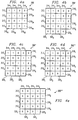
- Figure 3a is a representation of an initial array stored in the memory of Figure la and 1b.
- Figure 3b shows the data array of Figure 3a with an additional column and an additional row of flag bits.
- Figure 3c shows the data array of Figure 3b after a row inversion step.
- Figure 3d shows the data array of Figure 3c after a column inversion step, which is also a representation of a fully reorganized data array.
- Figure 4a is a representation of a second data array.
- Figure 4b shows the data array of Figure 4a with an additional column and an additional row of flag bits.
- Figure 4c shows the data array of Figure 4b after the row inversion step.
- Figure 4d shows the data array of Figure 4c after a column inversion step.
- Figure 4e shows the data array of the Figure 4d after a second row inversion step, which is also a representation of a fully reorganized array.
- Figure 5a is a circuit diagram of a memory storing the initial array in Figure 4a.
- Figure 5b is a circuit diagram of a memory according to an embodiment of the present invention, storing the reorganized array in Figure 4e.
- Figure 6a is a representation of a third initial array.
- Figure 6b shows the data array of Figure 6a divided into sections and with two additional columns and an additional row of flag bits.
- Figure 6c shows the data array of Figure 6b after a row inversion step.
- Figure 6d shows the data array of Figure 6c after a column inversion step, which is also a representation of a fully reorganized data array.
- Figure 7a is a circuit diagram of a memory storing the initial array in Figure 6a.
- Figure 7b is a circuit diagram of a memory according to an embodiment of the present invention, storing the reorganized array in Figure 6d.
- a memory according to an embodiment of the invention is designated generally by reference numeral 100.
- the memory 100 is for storing data content of an initial array 200, such as shown in Figure 3a, once it is reorganized into the reorganized array 200"', shown in Figure 3d.
- the initial array 200 has data cell bits 210 11 ... 210 44 of ones and zeros arranged in rows 212 1 ... 212 4 , and columns 214 1 ... 214 4 .
- the memory 100 is a programmable memory, such a ROM, EPROM, EEPROM, or even a programmable logic array (PLA), or any other memory that can be used in applications where specific customized data, typically in the form of a data array, is required for the operation of the application and the data array will not change with the use of the application.
- the memory 100 can be used in any application where the above memories are used, such as computers, game cartridges, encoders, and decoders.
- the memory 100 has data circuit array 104 that has a plurality of memory cells 110 11 ... 110 44 for storing the data in the reorganized array 200"', output circuitry for reading the data from the data circuit array, and address circuitry for sequentially addressing memory cells to read data from the memory.
- the memory cells 110 11 ... 110 44 are arranged in rows 112 1 ... 112 4 and columns 114 1 ... 114 4 . Although only four rows and columns of data cells, and 16 bits are shown many more can be and typically used in the data array; and although only four rows and columns of the data circuit array, and sixteen memory cells are shown many more can, and typically are, used in the memory.
- the memory also contains logic circuitry to enable the reading of the reorganized array from the memory to reproduce the information content of the initial array.
- the logic circuitry includes a plurality of flag memory cell 130 1 ... 130 4 arranged in rows and in one or more columns 132, each row corresponding to one memory row 112 1 ... 112 4 , and an exclusive OR gate, commonly referred to as an XOR gate, 120 1 ... 120 4 .
- One XOR gate 120 1 ... 120 4 is coupled to one ofthe memory columns 112 1 ... 112 4 .
- Each of the XOR gates has a first input 140 1 ... 140 4 coupled to one of the memory columns 112 1 ... 112 4 , a second input 142 1 ... 142 4 coupled to the flag column, and an output 144 1 ... 144 4 .
- the XOR gates invert the bits in the memory cells responsive to flag data in the corresponding flag memory cell.
- the logic circuitry also includes a row of inverters 122 1 ... 122 4
- the inverters are selectively coupled to the columns of the data circuit array when the flag data corresponding to the column is a one.
- the input of the inverter circuit is connected to the output 144 1 ... 144 4 of the XOR gate corresponding to the column in the data circuit array to which the inverter is connected.
- the inverters 122 1 ... 122 4 are connected between the column of the data circuit array and the first input 140 1 ... 140 4 of the XOR gate.
- the output circuitry contains a plurality of bit-lines 116 1 ... 116 4
- the address circuitry contains a plurality of wordlines 118 1 ... 118 4 .
- the bit-lines 116 1 ... 116 4 are used to read the contents of the memory cells 110 11 ... 110 44 .
- the wordlines are used to select the appropriate memory cell 110 11 ... 110 44 to be read. All of the memory cells in one memory column that are going to be coupled to a bit-line are coupled to one bit-line. Typically there is one bit-line 116 1 ... 116 4 for every memory column 114 1 ... 114 4 , however each bit-line 116 1 ... 116 4 can be used to read the data from multiple memory columns as described in U.S. Patent No.
- Memory cells 110 14, 110 33, 110 42 that store a one contain a transistor coupled to the bit-line.
- the rest of the memory cells do not have a transistor manufactured in those cells as shown in Figure 2a, or more likely, as shown in Figure 2b, have a transistor that is not connected to the bit-line, or have a transistor that is disabled such that it is permanently non-conductive. If the memory is to be pre-prepared than every memory cell will have a transistor but only the memory cells that store ones will be connected to bit-lines. If the memory is custom manufactured for the data array and is completely manufactured after the data array is available, the memory cell that will store zeros will not have transistors manufactured in them at all.
- the output circuitry also contains a flag bit-line 134. All of the flag memory cells in one column of flag memory cells that are going to be coupled to a bit-line are coupled to one flag bit-line. The data in the flag memory cells is read through the flag bit-lines. Each flag memory cell storing a one 130 2 has a transistor coupled to the flag bit-line 134.
- the inverters allows the memory to store a reorganized array that has much fewer ones than the initial array.
- the memory can have either the flag memory cell and XOR gate, or the inverters. This will still allow the memory to store a reorganized array that has fewer ones than the initial array, but in most cases more ones than a data array that can be stored in a memory with both (1) the flag memory cells and XOR gates, and (2) the inverters.
- the initial array 200 is provided, and then encoded to get the reorganized array 200"' and flag data.
- the flag data produced in encoding the initial array is recorded.
- the reorganized array is stored in the data circuit array and the flag data is stored in the flag memory cells.
- the rest of the logic circuitry is connected to the data circuit array based on the flag data.
- a row of column logic cells 220 1 ... 220 4 is identified for storing the flag data produced in encoding each of the columns of initial array.
- a column of row logic cells 218 1 ... 218 4 is identified for storing the flag data produced in encoding each of the row of the initial array.
- the data cell of the column logic cells 220 1 ... 220 4 and of the row logic cells 218 1 ... 218 4 are initially set to zero.
- the order of checking and inverting the rows and columns can be reversed, the columns can be checked and inverted first and then the rows can be checked and inverted.
- the inverters 122 1 ... 122 4 should be coupled between the columns of the data circuit array 114 1 ... 114 4 and the first input of the XOR gates 140 1 . .. 140 4 .
- the initial array 200 of Figure 3a is shown as stored in memory 8 in Figure 1a, the reorganized array 200"' is stored in the memory 100 of Figure 2a.
- the memory 100 of the current invention requires far fewer transistors connected to bit-lines than conventional memory 8.
- the reorganization has reduced the number of ones by more than half, therefore less than half as many transistors connected to bit-lines are needed with the memory 100 of the invention then were needed with a conventional memory 8. This allows the memory 100 of the current invention to draw much less power since the power consumption of the memory is proportional to the number of ones stored. It also allows the memory 100 of the current invention to have quicker access time to the individual memory cell, because now no row or column has more ones than zeros, and the access time is based on the number of ones in the row and the column of the memory cell.
- memory 100 can contain just the flag memory cell and XOR gates or just the inverters.
- the reorganized array is produced by just inverting the data in each of the rows of the initial array having more ones than zeros.
- the reorganized array is produced by just inverting the data in each of the columns of the initial array that has more ones than zeros.
- All of the encoding and recording are preferably preformed by software and the reorganized array is then input into a ROM generator to generate the layout of the memory.
- the initial array 600 can be reorganized to have even fewer ones if the initial array is divided into sections 630, 632.
- Each section contains a certain number of data columns, such that each of the rows is divided along these sections, producing data row sections 626 1 ... 626 4 and 628 1 ...628 4 .
- the sections 626 1 ... 626 4 , and 628 1 ...628 4 can be any size.
- Each section in a row can contain a different number data cell, for example one section of one row can have three data cells and another can have five data cells.
- the sections are produced by dividing the array into columns, the respective sections will have the same number of data cells in every row, for example the X th section 626 row#X of each row will have the same number of data bits.
- the initial array does not need to be divided up to be reorganized, such as the initial arrays in Figure 3 and 4 described above the initial array has just one section, and the sections of each row are the rows, respectively.
- a section can contain data in the first, third and fourth columns, but not in the second column.
- one column of row logic cells is provided for each section of the initial array, such that row logic cell corresponds to one section of the row of the initial array. Therefore, there is one column of row logic cells 634 1 ...634 4 corresponding to one section 630 and another column of row logic cells 636 1 ... 636 4 corresponding to another section 632.
- the flag memory cells are also arranged in rows, one row of flag memory cells 132 1 ... 132 4 and 136 1 ... 136 4 for each section of the initial array to store the row logic cells 634 1 ... 634 4 and 636 1 ... 636 4 , respectively.
- there is one flag bit-line 134, 138 for every column of flag memory cells 132 1 ...
- each flag bit-line can be used to read the data from multiple flag columns.
- Each of the flag bit-lines is connected to the second input of the XOR gate that corresponds to the column of the data circuit array that stores the column of the reorganized array to which the flag data corresponds.
- an initial array 600 shown in Figure 6a.
- This is initial array is divided into sections 630, 632 each section is encoded in the same manner described above for the encoding of the initial array to get a reorganized array 600"' shown in Figure 6c, and the flag data produced in encoding is recorded.
- the reorganized array is stored in the data circuit array and the flag data is stored in the flag memory cells.
- the rest of the logic circuitry is connected to the data circuit array based on the flag data.
- inverters 150, 152 can be added to the columns of flag memory cells and the data in each column of flag memory cells 136 1 ...136 4 that has more ones than zeros can be inverted and the column of flag memory cells 136 1 ...136 4 connected to the inverter 152.
- All of the encoding and recording are preferably preformed by sofware and the reorganized array is then input into a ROM generator to generate the layout of the memory.
- the number of section of the initial array and therefore the number of columns of flag memory cells is determined based on logically optimizing the data array to contain the fewest number of ones verses the additional cost of adding a flag column to the memory.
- Logically optimizing the data array is done by determining which data columns can be grouped together to produce the smallest number of ones, including the ones that will be needed as flag bits.
- the columns of the initial array do not have to be adjacent to be grouped together, and each grouping of columns, i.e. each section, does not have to have the same number of columns. This is typically performed in software, and can be performed using any known algorithm to do so, including an exhaustive search. Determining the optimum number of sections and adding the appropriate number of columns of flag memory cells is only possible if the memory is manufactured specifically for the application. If the memory was pre-prepared the number of flag columns would be set and it would not be possible to add additional flag columns.
- the number of columns of the flag memory cells can be preset.
- the number of sections of the initial array is set to the number of flag columns.
- reorganizing the initial array is done by determining which columns of the initial array can be grouped together into the available number of sections, or into fewer section, to produce the smallest number of ones, including the ones that will be needed as flag bits.
- the columns do not have to be adjacent to be grouped together, and each grouping of columns, i.e. each section, does not have to have the same number of columns. This is also typically performed in software, and can be performed using any known algorithm to do so, including an exhaustive search. Having the number of sections predetermined allows the initial array to be reorganized while still allowing the memory to be pre-prepared and programmed toward the end of the manufacturing process, or even to be programmed in the field for memories such as EEPROMs.
- a method that allows an initial array to be reorganized by reducing the number of ones in the array, and the memory that is used to store the reorganized array produces a memory with a reduced power consumption for quicker access time. Reducing the number of ones that need to be stored by inverting some of bits and adding circuitry to insure that the bits are read out to generate the information content of the initial array produces a memory that requires far fewer transistors connected to bit-lines than conventional memory. This allows the memory 100 of the current invention to draw much less power since the power consumption of the memory is proportional to the number of one in the array. It also allow the memory 100 of the current invention to have quicker access time to the individual memory cell, because now no row or column has more ones than zeros, and the access time is based on the number of ones in the row and the column of the memory cell.
Landscapes
- Read Only Memory (AREA)
- Static Random-Access Memory (AREA)
Applications Claiming Priority (2)
| Application Number | Priority Date | Filing Date | Title |
|---|---|---|---|
| US969890 | 1992-10-30 | ||
| US08/969,890 US5940332A (en) | 1997-11-13 | 1997-11-13 | Programmed memory with improved speed and power consumption |
Publications (2)
| Publication Number | Publication Date |
|---|---|
| EP0917154A2 true EP0917154A2 (de) | 1999-05-19 |
| EP0917154A3 EP0917154A3 (de) | 1999-11-03 |
Family
ID=25516126
Family Applications (1)
| Application Number | Title | Priority Date | Filing Date |
|---|---|---|---|
| EP98309093A Withdrawn EP0917154A3 (de) | 1997-11-13 | 1998-11-06 | Programmierter Speicher mit verbesserter Geschwindigkeit und Leistungsverbrauch |
Country Status (3)
| Country | Link |
|---|---|
| US (1) | US5940332A (de) |
| EP (1) | EP0917154A3 (de) |
| JP (1) | JPH11242895A (de) |
Cited By (5)
| Publication number | Priority date | Publication date | Assignee | Title |
|---|---|---|---|---|
| EP1130600A1 (de) * | 2000-03-01 | 2001-09-05 | Hewlett-Packard Company, A Delaware Corporation | Datenverteilungsabbildung für Festkörperspeicher |
| WO2002015192A1 (fr) * | 2000-08-17 | 2002-02-21 | Xemics Sa | Module de controle comprenant une memoire morte a consommation electrique reduite |
| WO2009019284A1 (en) * | 2007-08-09 | 2009-02-12 | International Business Machines Corporation | Providing energy reduction when storing data in a memory |
| US20090276650A1 (en) * | 2008-05-02 | 2009-11-05 | Canon Kabushiki Kaisha | Information processing apparatus and method for controlling information processing apparatus |
| DE102006061877B4 (de) * | 2005-12-28 | 2015-05-13 | Intel Corporation | Chip mit einer Speicherschaltung mit räumlich kodiertem Datenspeicher |
Families Citing this family (41)
| Publication number | Priority date | Publication date | Assignee | Title |
|---|---|---|---|---|
| US6768165B1 (en) | 1997-08-01 | 2004-07-27 | Saifun Semiconductors Ltd. | Two bit non-volatile electrically erasable and programmable semiconductor memory cell utilizing asymmetrical charge trapping |
| US6614692B2 (en) | 2001-01-18 | 2003-09-02 | Saifun Semiconductors Ltd. | EEPROM array and method for operation thereof |
| US6665769B2 (en) * | 2001-04-05 | 2003-12-16 | Saifun Semiconductors Ltd. | Method and apparatus for dynamically masking an N-bit memory array having individually programmable cells |
| US6584017B2 (en) | 2001-04-05 | 2003-06-24 | Saifun Semiconductors Ltd. | Method for programming a reference cell |
| US6594184B2 (en) * | 2001-09-06 | 2003-07-15 | Sun Microsystems, Inc. | System and method for accessing a memory array which tolerates non-exclusive read select enables |
| US6700818B2 (en) | 2002-01-31 | 2004-03-02 | Saifun Semiconductors Ltd. | Method for operating a memory device |
| US6917544B2 (en) | 2002-07-10 | 2005-07-12 | Saifun Semiconductors Ltd. | Multiple use memory chip |
| US6963505B2 (en) * | 2002-10-29 | 2005-11-08 | Aifun Semiconductors Ltd. | Method circuit and system for determining a reference voltage |
| US7136304B2 (en) | 2002-10-29 | 2006-11-14 | Saifun Semiconductor Ltd | Method, system and circuit for programming a non-volatile memory array |
| US6992932B2 (en) | 2002-10-29 | 2006-01-31 | Saifun Semiconductors Ltd | Method circuit and system for read error detection in a non-volatile memory array |
| JP3935139B2 (ja) | 2002-11-29 | 2007-06-20 | 株式会社東芝 | 半導体記憶装置 |
| US6967896B2 (en) | 2003-01-30 | 2005-11-22 | Saifun Semiconductors Ltd | Address scramble |
| US7178004B2 (en) | 2003-01-31 | 2007-02-13 | Yan Polansky | Memory array programming circuit and a method for using the circuit |
| US7142464B2 (en) | 2003-04-29 | 2006-11-28 | Saifun Semiconductors Ltd. | Apparatus and methods for multi-level sensing in a memory array |
| US7123532B2 (en) | 2003-09-16 | 2006-10-17 | Saifun Semiconductors Ltd. | Operating array cells with matched reference cells |
| US7652930B2 (en) | 2004-04-01 | 2010-01-26 | Saifun Semiconductors Ltd. | Method, circuit and system for erasing one or more non-volatile memory cells |
| US7755938B2 (en) * | 2004-04-19 | 2010-07-13 | Saifun Semiconductors Ltd. | Method for reading a memory array with neighbor effect cancellation |
| US7317633B2 (en) | 2004-07-06 | 2008-01-08 | Saifun Semiconductors Ltd | Protection of NROM devices from charge damage |
| US7095655B2 (en) | 2004-08-12 | 2006-08-22 | Saifun Semiconductors Ltd. | Dynamic matching of signal path and reference path for sensing |
| US7638850B2 (en) | 2004-10-14 | 2009-12-29 | Saifun Semiconductors Ltd. | Non-volatile memory structure and method of fabrication |
| US7257025B2 (en) * | 2004-12-09 | 2007-08-14 | Saifun Semiconductors Ltd | Method for reading non-volatile memory cells |
| US7535765B2 (en) | 2004-12-09 | 2009-05-19 | Saifun Semiconductors Ltd. | Non-volatile memory device and method for reading cells |
| CN1838323A (zh) | 2005-01-19 | 2006-09-27 | 赛芬半导体有限公司 | 可预防固定模式编程的方法 |
| US8053812B2 (en) | 2005-03-17 | 2011-11-08 | Spansion Israel Ltd | Contact in planar NROM technology |
| US8400841B2 (en) | 2005-06-15 | 2013-03-19 | Spansion Israel Ltd. | Device to program adjacent storage cells of different NROM cells |
| EP1746645A3 (de) | 2005-07-18 | 2009-01-21 | Saifun Semiconductors Ltd. | Speicherzellenanordnung mit sub-minimalem Wortleitungsabstand und Verfahren zu deren Herstellung |
| US7668017B2 (en) | 2005-08-17 | 2010-02-23 | Saifun Semiconductors Ltd. | Method of erasing non-volatile memory cells |
| US7221138B2 (en) | 2005-09-27 | 2007-05-22 | Saifun Semiconductors Ltd | Method and apparatus for measuring charge pump output current |
| US7352627B2 (en) | 2006-01-03 | 2008-04-01 | Saifon Semiconductors Ltd. | Method, system, and circuit for operating a non-volatile memory array |
| US7808818B2 (en) | 2006-01-12 | 2010-10-05 | Saifun Semiconductors Ltd. | Secondary injection for NROM |
| US8253452B2 (en) | 2006-02-21 | 2012-08-28 | Spansion Israel Ltd | Circuit and method for powering up an integrated circuit and an integrated circuit utilizing same |
| US7692961B2 (en) | 2006-02-21 | 2010-04-06 | Saifun Semiconductors Ltd. | Method, circuit and device for disturb-control of programming nonvolatile memory cells by hot-hole injection (HHI) and by channel hot-electron (CHE) injection |
| US7760554B2 (en) | 2006-02-21 | 2010-07-20 | Saifun Semiconductors Ltd. | NROM non-volatile memory and mode of operation |
| US7638835B2 (en) | 2006-02-28 | 2009-12-29 | Saifun Semiconductors Ltd. | Double density NROM with nitride strips (DDNS) |
| US7701779B2 (en) | 2006-04-27 | 2010-04-20 | Sajfun Semiconductors Ltd. | Method for programming a reference cell |
| US7605579B2 (en) | 2006-09-18 | 2009-10-20 | Saifun Semiconductors Ltd. | Measuring and controlling current consumption and output current of charge pumps |
| TWI493556B (zh) * | 2006-12-22 | 2015-07-21 | Sidense Corp | 用於混合式記憶體陣列之遮罩可編程及反熔絲架構 |
| US8120989B2 (en) * | 2007-06-25 | 2012-02-21 | Qualcomm Incorporated | Concurrent multiple-dimension word-addressable memory architecture |
| US7590001B2 (en) | 2007-12-18 | 2009-09-15 | Saifun Semiconductors Ltd. | Flash memory with optimized write sector spares |
| US7978493B1 (en) * | 2008-09-18 | 2011-07-12 | Altera Corporation | Data encoding scheme to reduce sense current |
| KR20110100739A (ko) * | 2010-03-05 | 2011-09-15 | 삼성전자주식회사 | 불휘발성 메모리 장치의 동작 방법, 컨트롤러의 동작 방법, 그리고 불휘발성 메모리 장치 및 컨트롤러를 포함하는 메모리 시스템의 동작 방법 |
Family Cites Families (15)
| Publication number | Priority date | Publication date | Assignee | Title |
|---|---|---|---|---|
| JPS56156993A (en) * | 1980-05-08 | 1981-12-03 | Fujitsu Ltd | Read only memory |
| FR2583203B1 (fr) * | 1985-06-11 | 1991-06-21 | Efcis | Memoire morte a capacite de ligne optimisee et procede d'encodage d'une telle memoire |
| JPS6271096A (ja) * | 1985-09-25 | 1987-04-01 | Toshiba Corp | 半導体集積回路装置 |
| US4760555A (en) * | 1986-04-21 | 1988-07-26 | Texas Instruments Incorporated | Memory array with an array reorganizer |
| IT1231902B (it) * | 1987-10-20 | 1992-01-15 | Sgs Microelettronica Spa | Memoria elettronica cmos di sola lettura a funzionamento statico |
| US5046045A (en) * | 1990-03-16 | 1991-09-03 | Chipware, Inc. | Method of storing data in a read only memory to enhance access time |
| IT1253680B (it) * | 1991-08-30 | 1995-08-22 | St Microelectronics Srl | Decodificatore per rom di tipo nand |
| US5297029A (en) * | 1991-12-19 | 1994-03-22 | Kabushiki Kaisha Toshiba | Semiconductor memory device |
| EP0575688B1 (de) * | 1992-06-26 | 1998-05-27 | STMicroelectronics S.r.l. | Programmierung von LDD-ROM-Zellen |
| US5377153A (en) * | 1992-11-30 | 1994-12-27 | Sgs-Thomson Microelectronics, Inc. | Virtual ground read only memory circuit |
| JPH06332797A (ja) * | 1993-05-27 | 1994-12-02 | Nec Corp | 半導体メモリ装置 |
| US5513136A (en) * | 1993-09-27 | 1996-04-30 | Intel Corporation | Nonvolatile memory with blocks and circuitry for selectively protecting the blocks for memory operations |
| US5642322A (en) * | 1995-05-24 | 1997-06-24 | Kawasaki Steel Corporation | Layout of semiconductor memory and content-addressable memory |
| JPH09120693A (ja) * | 1995-08-22 | 1997-05-06 | Mitsubishi Electric Corp | 半導体記憶装置 |
| JPH10302490A (ja) * | 1997-04-25 | 1998-11-13 | Mitsubishi Electric Corp | 読み出し専用半導体記憶装置 |
-
1997
- 1997-11-13 US US08/969,890 patent/US5940332A/en not_active Expired - Lifetime
-
1998
- 1998-11-06 EP EP98309093A patent/EP0917154A3/de not_active Withdrawn
- 1998-11-13 JP JP32394698A patent/JPH11242895A/ja active Pending
Cited By (12)
| Publication number | Priority date | Publication date | Assignee | Title |
|---|---|---|---|---|
| EP1130600A1 (de) * | 2000-03-01 | 2001-09-05 | Hewlett-Packard Company, A Delaware Corporation | Datenverteilungsabbildung für Festkörperspeicher |
| WO2001065562A1 (en) | 2000-03-01 | 2001-09-07 | Hewlett-Packard Company | Data balancing scheme in solid state storage devices |
| US6549446B2 (en) | 2000-03-01 | 2003-04-15 | Hewlett-Packard Company | Data balancing scheme in solid state storage devices |
| WO2002015192A1 (fr) * | 2000-08-17 | 2002-02-21 | Xemics Sa | Module de controle comprenant une memoire morte a consommation electrique reduite |
| US7107387B2 (en) | 2000-08-17 | 2006-09-12 | Semtech Neuchatel Sa | Control module comprising a ROM with reduced electrical consumption |
| DE102006061877B4 (de) * | 2005-12-28 | 2015-05-13 | Intel Corporation | Chip mit einer Speicherschaltung mit räumlich kodiertem Datenspeicher |
| WO2009019284A1 (en) * | 2007-08-09 | 2009-02-12 | International Business Machines Corporation | Providing energy reduction when storing data in a memory |
| US7783846B2 (en) | 2007-08-09 | 2010-08-24 | International Business Machines Corporation | Method, apparatus and computer program product providing energy reduction when storing data in a memory |
| JP2010536080A (ja) * | 2007-08-09 | 2010-11-25 | インターナショナル・ビジネス・マシーンズ・コーポレーション | データをメモリに格納するときのエネルギー削減の方法 |
| CN101765885B (zh) * | 2007-08-09 | 2013-10-23 | 国际商业机器公司 | 操作存储器件的方法和设备 |
| US20090276650A1 (en) * | 2008-05-02 | 2009-11-05 | Canon Kabushiki Kaisha | Information processing apparatus and method for controlling information processing apparatus |
| US8176346B2 (en) * | 2008-05-02 | 2012-05-08 | Canon Kabushiki Kaisha | Information processing apparatus with power saving mode and method for controlling information processing apparatus |
Also Published As
| Publication number | Publication date |
|---|---|
| EP0917154A3 (de) | 1999-11-03 |
| JPH11242895A (ja) | 1999-09-07 |
| US5940332A (en) | 1999-08-17 |
Similar Documents
| Publication | Publication Date | Title |
|---|---|---|
| US5940332A (en) | Programmed memory with improved speed and power consumption | |
| US4958377A (en) | Character string identification device with a memory comprising selectively accessible memory areas | |
| US5691945A (en) | Technique for reconfiguring a high density memory | |
| JP4726098B2 (ja) | 連想メモリ符号化出力 | |
| US4964078A (en) | Combined multiple memories | |
| US5555397A (en) | Priority encoder applicable to large capacity content addressable memory | |
| US5717901A (en) | Variable depth and width memory device | |
| CN1612265B (zh) | 半导体存储设备 | |
| US6002607A (en) | Read-only-memory (ROM) having a memory cell that stores a plurality of bits of information | |
| US4845668A (en) | Variable field content addressable memory | |
| US5854763A (en) | Integrated circuit with non-binary decoding and data access | |
| JP3280214B2 (ja) | シリアルアクセスメモリの予測読出し方法及びそのためのメモリ | |
| MY130268A (en) | Three-dimensional memory array and method for storing data bits and ecc bits therein | |
| US5250859A (en) | Low power multifunction logic array | |
| US6169685B1 (en) | Content addressable memories | |
| US5598365A (en) | High-density read-only memory | |
| US5745401A (en) | High-speed programmable read only memory | |
| US6424556B1 (en) | System and method for increasing performance in a compilable read-only memory (ROM) | |
| US4744053A (en) | ROM with mask programmable page configuration | |
| US5309045A (en) | Configurable logic element with independently clocked outputs and node observation circuitry | |
| US5231603A (en) | Variable page ROM | |
| US4975882A (en) | User programmable redundant memory | |
| CN100505096C (zh) | 用于多级单元存储器的方法与系统 | |
| US5793684A (en) | Memory device having selectable redundancy for high endurance and reliability and method therefor | |
| US5603023A (en) | Processor circuit for heapsorting |
Legal Events
| Date | Code | Title | Description |
|---|---|---|---|
| PUAI | Public reference made under article 153(3) epc to a published international application that has entered the european phase |
Free format text: ORIGINAL CODE: 0009012 |
|
| AK | Designated contracting states |
Kind code of ref document: A2 Designated state(s): DE FR GB IT |
|
| AX | Request for extension of the european patent |
Free format text: AL;LT;LV;MK;RO;SI |
|
| PUAL | Search report despatched |
Free format text: ORIGINAL CODE: 0009013 |
|
| AK | Designated contracting states |
Kind code of ref document: A3 Designated state(s): AT BE CH CY DE DK ES FI FR GB GR IE IT LI LU MC NL PT SE |
|
| AX | Request for extension of the european patent |
Free format text: AL;LT;LV;MK;RO;SI |
|
| RIC1 | Information provided on ipc code assigned before grant |
Free format text: 6G 11C 17/00 A, 6G 11C 7/00 B |
|
| 17P | Request for examination filed |
Effective date: 20000422 |
|
| AKX | Designation fees paid |
Free format text: DE FR GB IT |
|
| STAA | Information on the status of an ep patent application or granted ep patent |
Free format text: STATUS: THE APPLICATION HAS BEEN WITHDRAWN |
|
| 18W | Application withdrawn |
Withdrawal date: 20021118 |